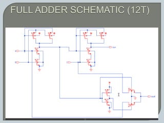
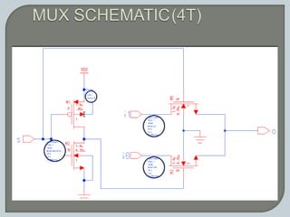
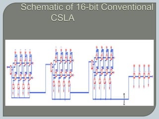
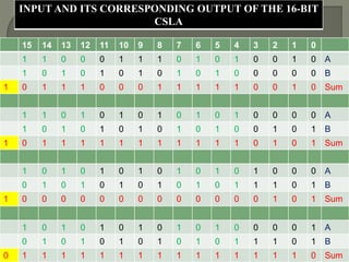
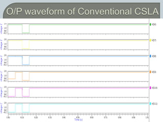
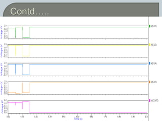
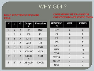
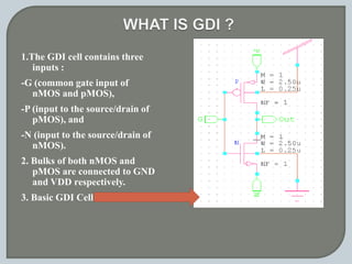
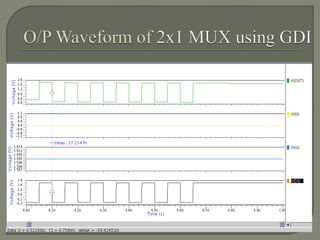
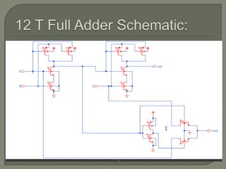
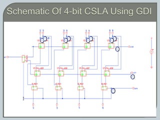
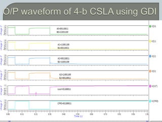
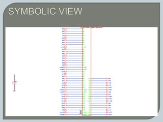
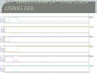
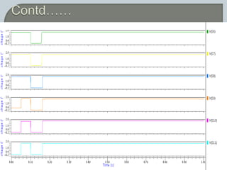
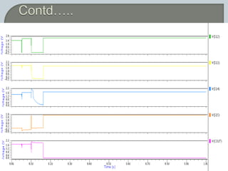
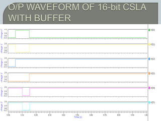
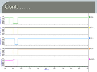
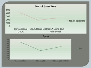
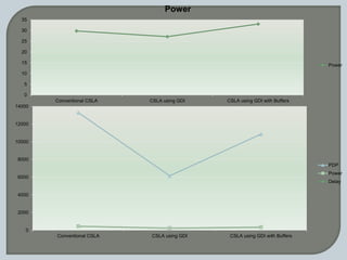
Gate Diffusion Input Technology (Very Large Scale Integration)Ashwin Shroff
The aim of project is by using GDI technique the power consumption, delay, chip area and connection and parasitic capacitors is decreased. In this project, we are implementing the new T-flip flop using GDI technique for low power and high speed in order to achieve power delay product (PDP)
A comparative study of full adder using static cmos logic styleeSAT Publishing House
IJRET : International Journal of Research in Engineering and Technology is an international peer reviewed, online journal published by eSAT Publishing House for the enhancement of research in various disciplines of Engineering and Technology. The aim and scope of the journal is to provide an academic medium and an important reference for the advancement and dissemination of research results that support high-level learning, teaching and research in the fields of Engineering and Technology. We bring together Scientists, Academician, Field Engineers, Scholars and Students of related fields of Engineering and Technology.
Study on self resetting logic with gate diffusion input (SRL-GDI)shubham jha
With continual technology scaling and improvements in lithography, the integrated system has become faster and thus it is employed in diverse real-time applications. To support high performance applications, proper choice of technology selection and topology for implementing various logic are the mandatory issues in designing low- power devices.
Self Resetting Logic with Gate Diffusion Input (SRLGDI) is the successor of SRCMOS where the CMOS block is replaced with the GDI block hence the name SRLGDI, which is an asynchronous dynamic circuit. This logic family resolves the issues in dynamic circuits like charge sharing , charge leakage , short circuit power dissipation, monotonicity requirement and low output voltage.
In this design the pull down tree is implemented with gate diffusion input (GDI) with level restoration which apparently eliminates the conductance overlap between nMOS and pMOS devices , thereby reducing the short circuit power dissipation and providing high output voltage.
The rapid growth in the use of portable system has triggered the research effort in low power microelectronic. This is due to the fact that the battery technology is not increasing with the same pace as the microelectronics technology. Only a limited power is available for the mobile system. Therefore low power design has become a major design consideration. Modified Gate Diffusion Input (MGDI) is a low power design which is a modification of Gate Diffusion Input (GDI).GDI is the lowest design technique, which is suitable for designing fast, low power circuit using reduced number of transistor. The main drawback associated with GDI is that the bulk terminal is not properly biased thereby the circuit exhibits threshold drop and it can be fabricated only in Twin well CMOS or Silicon on Insulator (SOI) process. So to overcome this MGDI is introduced.
Design of low power cmos logic circuits using gate diffusion input (gdi) tech...VLSICS Design
The Gate diffusion input (GDI) is a novel technique
for low power digital circuit design. This techniq
ue
reduces the power dissipation, propagation delay, a
rea of digital circuits and it maintains low comple
xity
of logic design. In this paper, the 4×1 Multiplexer
, 8×3 Encoder, BCD Counter and Mealy State Machine
were implemented by using Pass Transistors (PT), Tr
ansmission Gate (TG) and Gate Diffusion Input (GDI)
technique and then they were compared with each oth
er for power dissipation. The Multiplexers and
Encoders are combinational circuits and Counters an
d mealy machines are sequential circuits both of th
em
are very important digital systems so power optimiz
ation should be done to those digital circuits. The
whole processes for development of digital circuits
and simulation was done by using the mentor graphi
cs
backend tool. This method can also be extended to t
he processors and other high level designs for
optimization of power dissipation, area and delay i
n order to increase the circuit efficiency.
This paper presents a recursive designing approach for high energy efficient carry select adder (CSA). Nowadays, the portable equipment’s like mobile phones and laptops have higher demands in the market. So, the designers must focus greater attention while designing such devices. Which means that have the devices must have lesser power consumption, low cost and have a better performance. The customers mainly focus on the equipment’s which have lesser power consumption, low cost and better performance. As we all know that the adders are the basic building block of microprocessors. The performance of the adders greatly influences the performance of those processors. The carry select adder is most suitable among other adders which have fast addition operation at low cost. The carry select adder (CSA) consists of chain full adders (FAs) and multiplexers. Here a carry select adder is designed with four FAs and four multiplexers. The proposed structure is assessed by the power consumption of the carry select adder using a 32-nm static CMOS technology for a wide range of supply voltages. The simulation results are obtained using Tanner EDA which reveals that the carry select adder has low power consumption.
A Low power and area efficient CLA adder design using Full swing GDI techniqueIJERA Editor
The low power VLSI design has an important role in designing of many electronic systems. While designing
any combinational or sequential circuits, the important parameters like power consumption, implementation
area, voltage leakage and performance of the circuit are to be considered. Design of area, high speed and powerefficient
data path logic systems forms the largest areas of research in VLSI system design. This paper presents
a low power Carry look ahead adder design using Full swing Gate diffusion (FS-GDI) technique. The proposed
CLA implementation utilizes improved full-swing GDI F1 and F2 gates, which are the counterparts of standard
CMOS NAND and NOR gates. The basic Gate Diffusion Input (GDI) logic style suffers from some practical
limitations like swing degradation, fabrication complexity in standard CMOS process and bulk connections.
These limitations can be overcome by Full swing GDI technique. The proposed technique utilizes a single swing
restoration (SR) transistor to improve the output swing of F1 and F2 GDI gates. A 16-bit CLA is designed and
Simulations are performed by Mentor graphics 130nm CMOS technology ELDO simulator. Simulation results
have shown a greater reduction in delay, power dissipation and area.
Highly -increasing requirement for mobile and several electronic devices want the use of VLSI circuits which are highly power efficient. The most primitive arithmetic operation in processors is addition and the adder is the most highly used arithmetic component of the processor. Carry Select Adder (CSA) is one of the fastest adders and the structure of the CSA shows that there is a possibility for increasing its efficiency by reducing the power dissipation and area in the CSA. This research paper presents power and delay analysis of various adders and proposed a 32-bit CSA that is implemented using variable size of the combination of adders, thus the proposed Carry select Adder (CSA) which has minimum Delay, and less power consumption hence improving the efficiency and speed of the Carry Select Adder.
DESIGN AND IMPLEMENTATION OF LOW POWER ALU USING CLOCK GATING AND CARRY SELEC...IAEME Publication
CPUs in general-purpose personal computers, such as desktops and laptops, dissipate significantly more power in the order of few watts because of their higher complexity and speed. ALU is a fundamental building block of CPU. It does all process related to arithmetic and logic operations. As the operations become more complex, the ALU become more complex, more expensive, takes up more space in the CPU and contributes more power dissipation within the CPU. Hence power consumption of ALU is a major issue in the designing of CPU.
Implementation of Low Power and Area Efficient Carry Select Adderinventionjournals
International Journal of Engineering and Science Invention (IJESI) is an international journal intended for professionals and researchers in all fields of computer science and electronics. IJESI publishes research articles and reviews within the whole field Engineering Science and Technology, new teaching methods, assessment, validation and the impact of new technologies and it will continue to provide information on the latest trends and developments in this ever-expanding subject. The publications of papers are selected through double peer reviewed to ensure originality, relevance, and readability. The articles published in our journal can be accessed online.
Design and Verification of Area Efficient Carry Select Adderijsrd.com
Carry Select Adder (CSLA) is one of the fastest adders used in many data-processing processors to perform fast arithmetic functions. From the structure of the CSLA, it is clear that there is scope for reducing the area and power consumption in the CSLA. This work uses a simple and efficient gate-level modification to significantly reduce the area and power of the CSLA. Based on this modification 16, 32 square - root CSLA (SQRT CSLA) architecture have been developed and compared with the regular SQRT CSLA architecture. The proposed design has reduced area and power as compared with the regular SQRT CSLA with only a slight increase in the delay. This work evaluates the performance of the proposed designs in terms of delay, area.
Area Delay Power Efficient and Implementation of Modified Square-Root Carry S...IJTET Journal
Abstract: In VLSI Technology, Carry Propagation Delay is the most important concern for the Adders. Adder is the most unavoidable component for the arithmetic performances. This paper is Modified Square Root-Carry Select Adder (SQRT-CSLA) design reduces the delay with 16 bit adder. Carry select adder have two units for Carry Generation (CG) and Carry Selection (CS). The modified SQRT-CSLA design can gives parallel path for carry propagation. So the overall adder delay has reduced. Modified design is obtained using Ripple Carry Adder (RCA) with Boolean Excess-1 Converter (BEC). BEC produces an output i.e., is an excess one result for given input bits. Then input bits and BEC output is given to multiplexer for carry selection. Use of BEC instead of dual RCA gives efficient carry propagation delay and it consumes the lower power and overall gates using in design is reduced with compared to carry select adder with dual RCA. The final sum is calculated using final sum generation.
Design and Implementation of Low-Power and Area-Efficient 64 bit CSLA using VHDLIJSRD
All processor consisting ALU and adder plays important role for design of ALU. Design of low area and power efficient adder helps to reduce power consumption and area of any processor. Now a day’s major area of research in VLSI system is design of area, high speed and low power data path logic systems. In digital adders, the speed of addition is restricted by the time necessary to send a carry signal through the adder. The area and power consumption is reduced by modifying regular CSLA architecture. The proposed architecture is developed with the help of a simple ripple carry adder (RCA) and gate-level architecture. It consists of single RCA which improves the performance of the proposed designs then the regular designs in terms of power consumption and area.
VLSI Projects for M. Tech, VLSI Projects in Vijayanagar, VLSI Projects in Bangalore, M. Tech Projects in Vijayanagar, M. Tech Projects in Bangalore, VLSI IEEE projects in Bangalore, IEEE 2015 VLSI Projects, FPGA and Xilinx Projects, FPGA and Xilinx Projects in Bangalore, FPGA and Xilinx Projects in Vijayangar
Implementation of Area Effective Carry Select AddersKumar Goud
Abstract: In the design of Integrated circuit area occupancy plays a vital role because of increasing the necessity of portable systems. Carry Select Adder (CSLA) is a fast adder used in data processing processors for performing fast arithmetic functions. From the structure of the CSLA, the scope is reducing the area of CSLA based on the efficient gate-level modification. In this paper 16 bit, 32 bit, 64 bit and 128 bit Regular Linear CSLA, Modified Linear CSLA, Regular Square-root CSLA (SQRT CSLA) and Modified SQRT CSLA architectures have been developed and compared. However, the Regular CSLA is still area-consuming due to the dual Ripple-Carry Adder (RCA) structure. For reducing area, the CSLA can be implemented by using a single RCA and an add-one circuit instead of using dual RCA. Comparing the Regular Linear CSLA with Regular SQRT CSLA, the Regular SQRT CSLA has reduced area as well as comparing the Modified Linear CSLA with Modified SQRT CSLA; the Modified SQRT CSLA has reduced area. The results and analysis show that the Modified Linear CSLA and Modified SQRT CSLA provide better outcomes than the Regular Linear CSLA and Regular SQRT CSLA respectively. This project was aimed for implementing high performance optimized FPGA architecture. Modelsim 10.0c is used for simulating the CSLA and synthesized using Xilinx PlanAhead13.4. Then the implementation is done in Virtex5 FPGA Kit.
Keywords: Field Programmable Gate Array (FPGA), efficient, Carry Select Adder (CSLA), Square-root CSLA (SQRTCSLA).
A High Speed Wallace Tree Multiplier Using Modified Booth Algorithm for Fast ...Kumar Goud
Abstract— Designing multipliers that are of high-speed, low power, and regular in layout are of substantial research interest. Speed of the multiplier can be increased by reducing the generated partial products. Many attempts have been made to reduce the number of partial products generated in a multiplication process; one of them is Wallace tree multiplier. Wallace Tree CSA structures have been used to sum the partial products in reduced time. In this paper Wallace tree construction is investigated and evaluated. Speed of traditional Wallace tree multiplier can be improved by using compressor techniques. In this paper Wallace tree is constructed by traditional method and with the help of compressor techniques such as 4:2 compressor, 5:2 compressor, 6:2 compressor, 7:2 compressor. Therefore, minimizing the number of half adders used in a multiplier reduction will reduce the complexity.
Index Terms—Component, formatting, style, styling, insert. (key words)
4 bit cmos full adder in submicron technology with low leakage and groun...shireesha pallepati
hai..this is my final year b.tech project on 4-bit CMOS full in sub micron technology for low lowkage and ground bounce noise reduction..feeling happy to share my presentation.
dedicated to my parents and faculty
MAC unit is used for high performance digital signal processing systems. The DSP applications include filtering, convolution, and inner products.
The design consists of 64 bit modified Wallace multiplier.
128 bit carry save adder and a register/ accumulator.
The output of carry save adder is 129 bit i.e. one bit is for the carry (128bits+ 1 bit). Then, the output is given to the accumulator register.
The accumulator register used in this design is Parallel In Parallel Out (PIPO).
The output of the accumulator register is taken out or fed back as one of the input to the carry save adder.
APPLICATIONS:
1) digital signal processing (DSP) applications
a. Signal filtering
b. convolution.
c. Decreasing number of inner products.
2) Optical communications.
The low power has been the main concern for the VLSI industry with the technology scaling in CMOS process from 130 nm to 22nm. The presentation here gives a brief idea about the several low power VLSI techniques being used in VLSI circuits to reduce the power and delay. for any query feel free to visit us at: http://www.siliconmentor.com/
Design and Implementation of Area Optimized, Low Complexity CMOS 32nm Technol...IJERA Editor
A numerically controlled oscillator (NCO) is a digital signal generator which is a very important block in many Digital Communication Systems such as Software Defined Radios, Digital Radio set and Modems, Down/Up converters for Cellular and PCS base stations etc. NCO creates a synchronous, discrete-time, discrete-valued representation of a sinusoidal waveform. This paper implements the development and design of CMOS look up Table based numerically controlled oscillator which improves the performance, reduces the power & area requirement. The design is implemented with CMOS 32 nm Technology with Microwind 3.8 software tool. In addition, it can be used for analog circuit also enables the integration of complete system on chip. This paper also describes the design of a NCO which is of contemporary nature with reasonable speed, resolution and linearity with lower power, low area. For all about Pre Layout simulation has been realized using 32nm CMOS process Technology.
Implementation of Area & Power Optimized VLSI Circuits Using Logic TechniquesIOSRJVSP
To achieve the reduction of power consumption, optimizations are required at various levels of the design steps such as algorithm, architecture, logic and circuit & process techniques. This paper considers the two logic level approaches for low power digital design. Optimization techniques are carried to reduce switching activity power of individual logic-gates. we can reduce the power by using either circuit level optimization or logical level optimization. In this paper, the circuit level optimization process is followed to reduce the area and power. In the first approach, Modified gate diffusion input (GDI) logic is used in the proposed parallel asynchronous self time adder (PASTA) technique. Similarly, the structure of XOR gate and half adder is reduced to achieve the low area and low power. In second approach, Multi value logic based digital circuit is designed by increasing the representation domain from the two level (N=2) switching algebra to N > 2 levels. The main advantage of this approach is to compensate the inefficiency of existing integrated circuits that are used to implement the universal set of MVL gates. From the results, the proposed GDL logic based Adder offers less number of transistors (area) and low power consumption than the existing technique. And proposed MVL technique allows designing MVL digital circuit that is set to obtain the values from the binary circuits. Also this technique offers low power and small wiring delay, when compared to binary and three value logic. The simulation process is carried out by tanner toolv14.11 to check the functionality of the PASTA & MVL circuits.
Optimization of Digitally Controlled Oscillator with Low Poweriosrjce
IOSR journal of VLSI and Signal Processing (IOSRJVSP) is a double blind peer reviewed International Journal that publishes articles which contribute new results in all areas of VLSI Design & Signal Processing. The goal of this journal is to bring together researchers and practitioners from academia and industry to focus on advanced VLSI Design & Signal Processing concepts and establishing new collaborations in these areas.
Design and realization of microelectronic systems using VLSI/ULSI technologies require close collaboration among scientists and engineers in the fields of systems architecture, logic and circuit design, chips and wafer fabrication, packaging, testing and systems applications. Generation of specifications, design and verification must be performed at all abstraction levels, including the system, register-transfer, logic, circuit, transistor and process levels
Complex digital and analog circuits and multiple clock signals used for design and development of modern systems usually make the job of engineers and designers a tedious one. While working with complex circuits and signals, a designer might encounter problems with circuit validation due to long simulation time. These complexities adversely affect the development time and hence increase time to market incurring higher production costs. By applying a new methodology in their Digital Phase-Locked Loop (Digital PLL) design, the engineers at QuEST reduced the simulation effort to one-by-third.
In digital logic and computing, a counter is a device which stores the number of times a particular event or process has occurred, often in relationship to a clock signal. CMOS devices are designed for high noise immunity and low static power consumption. CMOS accomplishes current reduction by complementing every nMOSFET with a pMOSFET and connecting both gates and both drains together. A high voltage on the gates will cause the nMOSFET to conduct and the pMOSFET to not conduct, while a low voltage on the gate causes the reverse. This arrangement greatly reduces power consumption and heat generation .Finally we proposed counter using SRAM model, provides the best resolution, high output current and good output-input current linearity.
128-Bit Area Efficient Reconfigurable Carry Select Adder ijcisjournal
Adders are one of the most critical arithmetic circuits in a system and their throughput affects the overall
performance of the system. Carry Select Adder (CSLA) is one of the fastest adders used in many dataprocessing
processors to perform fast arithmetic functions. From the structure of the CSLA, it is clear that
there is scope for reducing the area and power consumption in the CSLA. In this paper, we proposed an
area-efficient carry select adder by sharing the common Boolean logic term. After logic optimization and
sharing partial circuit, we only need one XOR gate and one inverter gate for sum generation. Through the
multiplexer, we can select the final-sum only and for carry selection we need only one AND gate and one
OR gate. Based on this modification 16-, 32-, 64-, and 128-bit CSLA architecture have been developed and
compared with the conventional CSLA architecture. The proposed design greatly reduces the area
compared to other CSLAs. From this improvement, the gate count of a 128-bit carry select adder can be
reduced from 3320 to 1664. The proposed structure is implemented in Artix-7 FPGA. Compared with the
proposed design, the conventional CSLA has 65.80% less area.
HEAP SORT ILLUSTRATED WITH HEAPIFY, BUILD HEAP FOR DYNAMIC ARRAYS.
Heap sort is a comparison-based sorting technique based on Binary Heap data structure. It is similar to the selection sort where we first find the minimum element and place the minimum element at the beginning. Repeat the same process for the remaining elements.
CW RADAR, FMCW RADAR, FMCW ALTIMETER, AND THEIR PARAMETERSveerababupersonal22
It consists of cw radar and fmcw radar ,range measurement,if amplifier and fmcw altimeterThe CW radar operates using continuous wave transmission, while the FMCW radar employs frequency-modulated continuous wave technology. Range measurement is a crucial aspect of radar systems, providing information about the distance to a target. The IF amplifier plays a key role in signal processing, amplifying intermediate frequency signals for further analysis. The FMCW altimeter utilizes frequency-modulated continuous wave technology to accurately measure altitude above a reference point.
Student information management system project report ii.pdfKamal Acharya
Our project explains about the student management. This project mainly explains the various actions related to student details. This project shows some ease in adding, editing and deleting the student details. It also provides a less time consuming process for viewing, adding, editing and deleting the marks of the students.
Welcome to WIPAC Monthly the magazine brought to you by the LinkedIn Group Water Industry Process Automation & Control.
In this month's edition, along with this month's industry news to celebrate the 13 years since the group was created we have articles including
A case study of the used of Advanced Process Control at the Wastewater Treatment works at Lleida in Spain
A look back on an article on smart wastewater networks in order to see how the industry has measured up in the interim around the adoption of Digital Transformation in the Water Industry.
Hierarchical Digital Twin of a Naval Power SystemKerry Sado
A hierarchical digital twin of a Naval DC power system has been developed and experimentally verified. Similar to other state-of-the-art digital twins, this technology creates a digital replica of the physical system executed in real-time or faster, which can modify hardware controls. However, its advantage stems from distributing computational efforts by utilizing a hierarchical structure composed of lower-level digital twin blocks and a higher-level system digital twin. Each digital twin block is associated with a physical subsystem of the hardware and communicates with a singular system digital twin, which creates a system-level response. By extracting information from each level of the hierarchy, power system controls of the hardware were reconfigured autonomously. This hierarchical digital twin development offers several advantages over other digital twins, particularly in the field of naval power systems. The hierarchical structure allows for greater computational efficiency and scalability while the ability to autonomously reconfigure hardware controls offers increased flexibility and responsiveness. The hierarchical decomposition and models utilized were well aligned with the physical twin, as indicated by the maximum deviations between the developed digital twin hierarchy and the hardware.
6th International Conference on Machine Learning & Applications (CMLA 2024)ClaraZara1
6th International Conference on Machine Learning & Applications (CMLA 2024) will provide an excellent international forum for sharing knowledge and results in theory, methodology and applications of on Machine Learning & Applications.
NO1 Uk best vashikaran specialist in delhi vashikaran baba near me online vas...Amil Baba Dawood bangali
Contact with Dawood Bhai Just call on +92322-6382012 and we'll help you. We'll solve all your problems within 12 to 24 hours and with 101% guarantee and with astrology systematic. If you want to take any personal or professional advice then also you can call us on +92322-6382012 , ONLINE LOVE PROBLEM & Other all types of Daily Life Problem's.Then CALL or WHATSAPP us on +92322-6382012 and Get all these problems solutions here by Amil Baba DAWOOD BANGALI
#vashikaranspecialist #astrologer #palmistry #amliyaat #taweez #manpasandshadi #horoscope #spiritual #lovelife #lovespell #marriagespell#aamilbabainpakistan #amilbabainkarachi #powerfullblackmagicspell #kalajadumantarspecialist #realamilbaba #AmilbabainPakistan #astrologerincanada #astrologerindubai #lovespellsmaster #kalajaduspecialist #lovespellsthatwork #aamilbabainlahore#blackmagicformarriage #aamilbaba #kalajadu #kalailam #taweez #wazifaexpert #jadumantar #vashikaranspecialist #astrologer #palmistry #amliyaat #taweez #manpasandshadi #horoscope #spiritual #lovelife #lovespell #marriagespell#aamilbabainpakistan #amilbabainkarachi #powerfullblackmagicspell #kalajadumantarspecialist #realamilbaba #AmilbabainPakistan #astrologerincanada #astrologerindubai #lovespellsmaster #kalajaduspecialist #lovespellsthatwork #aamilbabainlahore #blackmagicforlove #blackmagicformarriage #aamilbaba #kalajadu #kalailam #taweez #wazifaexpert #jadumantar #vashikaranspecialist #astrologer #palmistry #amliyaat #taweez #manpasandshadi #horoscope #spiritual #lovelife #lovespell #marriagespell#aamilbabainpakistan #amilbabainkarachi #powerfullblackmagicspell #kalajadumantarspecialist #realamilbaba #AmilbabainPakistan #astrologerincanada #astrologerindubai #lovespellsmaster #kalajaduspecialist #lovespellsthatwork #aamilbabainlahore #Amilbabainuk #amilbabainspain #amilbabaindubai #Amilbabainnorway #amilbabainkrachi #amilbabainlahore #amilbabaingujranwalan #amilbabainislamabad
Forklift Classes Overview by Intella PartsIntella Parts
Discover the different forklift classes and their specific applications. Learn how to choose the right forklift for your needs to ensure safety, efficiency, and compliance in your operations.
For more technical information, visit our website https://intellaparts.com
Cosmetic shop management system project report.pdfKamal Acharya
Buying new cosmetic products is difficult. It can even be scary for those who have sensitive skin and are prone to skin trouble. The information needed to alleviate this problem is on the back of each product, but it's thought to interpret those ingredient lists unless you have a background in chemistry.
Instead of buying and hoping for the best, we can use data science to help us predict which products may be good fits for us. It includes various function programs to do the above mentioned tasks.
Data file handling has been effectively used in the program.
The automated cosmetic shop management system should deal with the automation of general workflow and administration process of the shop. The main processes of the system focus on customer's request where the system is able to search the most appropriate products and deliver it to the customers. It should help the employees to quickly identify the list of cosmetic product that have reached the minimum quantity and also keep a track of expired date for each cosmetic product. It should help the employees to find the rack number in which the product is placed.It is also Faster and more efficient way.
About
Indigenized remote control interface card suitable for MAFI system CCR equipment. Compatible for IDM8000 CCR. Backplane mounted serial and TCP/Ethernet communication module for CCR remote access. IDM 8000 CCR remote control on serial and TCP protocol.
• Remote control: Parallel or serial interface.
• Compatible with MAFI CCR system.
• Compatible with IDM8000 CCR.
• Compatible with Backplane mount serial communication.
• Compatible with commercial and Defence aviation CCR system.
• Remote control system for accessing CCR and allied system over serial or TCP.
• Indigenized local Support/presence in India.
• Easy in configuration using DIP switches.
Technical Specifications
Indigenized remote control interface card suitable for MAFI system CCR equipment. Compatible for IDM8000 CCR. Backplane mounted serial and TCP/Ethernet communication module for CCR remote access. IDM 8000 CCR remote control on serial and TCP protocol.
Key Features
Indigenized remote control interface card suitable for MAFI system CCR equipment. Compatible for IDM8000 CCR. Backplane mounted serial and TCP/Ethernet communication module for CCR remote access. IDM 8000 CCR remote control on serial and TCP protocol.
• Remote control: Parallel or serial interface
• Compatible with MAFI CCR system
• Copatiable with IDM8000 CCR
• Compatible with Backplane mount serial communication.
• Compatible with commercial and Defence aviation CCR system.
• Remote control system for accessing CCR and allied system over serial or TCP.
• Indigenized local Support/presence in India.
Application
• Remote control: Parallel or serial interface.
• Compatible with MAFI CCR system.
• Compatible with IDM8000 CCR.
• Compatible with Backplane mount serial communication.
• Compatible with commercial and Defence aviation CCR system.
• Remote control system for accessing CCR and allied system over serial or TCP.
• Indigenized local Support/presence in India.
• Easy in configuration using DIP switches.
Industrial Training at Shahjalal Fertilizer Company Limited (SFCL)MdTanvirMahtab2
This presentation is about the working procedure of Shahjalal Fertilizer Company Limited (SFCL). A Govt. owned Company of Bangladesh Chemical Industries Corporation under Ministry of Industries.
2. Carry Select Adder (CSLA) is a fast adder which is
used in the data processing processors for performing fast
arithmetic operations.
The carry-select adder generally consists of two ripple
carry adders and multiplexers .
One RCA performs addition by assuming the input
carry is 0 and other RCA performs addition by assuming
the input carry is 1.
MUX select the output according to the carry from
previous stage
6. Paper Name Publisher Description
Implementation and
comparision of effective
area architecture of CSA.
R. Priya and J. Senthil Kumar “2013
IEEE International Conference on
emerging trends on computing
,communication and nano
technology(ICECCN2013).
This is the main paper in which
conventional CSLA has been
implemented
Low Power Digital design
using modified GDI
method.
Padmanabhan Balasubramanian and
Johince John,2006, IEEE.
This technique allows reducing
power consumption, propagation
delay, and area of digital circuits
GDI Technique : A
Power-Efficient Method
for Digital Circuits
.
Kunal & Nidhi Kedia Department
of Electronics &
Telecommunication Engineering,
Synergy Institute of Engineering &
Technology, Dhenkanal, Odisha
This paper describes the design and
implementation of various digital
circuit using GDI technique
22. 8 Transistor Full adder circuit is used.
MUX of 2 transistor is used.
The MUX and FA circuit is designed by using
GDI(gate diffusion input ) technique.
23. BASIC FUNCTIONS USING GDI
CELL
COMPARISON OF TRANSISTOR
COUNT OF GDI AND STATIC CMOS
N p G Outpu
t
Function
0 1 A A’ INV
0 B A A’B F1
B 1 A A’+B F2
1 B A A+B OR
B 0 A AB AND
C B A A’B+AC MUX
B’ B A A’B+B’
A
XOR
B B’ A AB+A’B
’
XNOR
fUNCTIO
N
GDI CMOS
INV 2 2
F1 2 6
F2 2 6
OR 2 6
AND 2 6
MUX 2 14
XOR 4 12
XNOR 4 12
NAND 4 4
NOR 4 4
24. 1.The GDI cell contains three
inputs :
-G (common gate input of
nMOS and pMOS),
-P (input to the source/drain of
pMOS), and
-N (input to the source/drain of
nMOS).
2. Bulks of both nMOS and
pMOS are connected to GND
and VDD respectively.
3. Basic GDI Cell
25.
26.
27.
28.
29.
30.
31.
32.
33.
34.
35.
36.
37.
38.
39.
40. CONVENTIONAL
CSLA
CSLA USING GDI
TECHNIQUE
(WITHOUT BUFFER)
CSLA USING GDI
TECHNIQUE
(WITH BUFFER)
NUMBER OF
TRANSISTO
R
408 186
(54.41 % Saved
186+64=250 (In
worst case)
(38.72 %Saved)
DELAY 430.45 pS 217.35 pS
(49.50% Faster)
318.18 pS
(26.08 % Faster)
POWER 29.82 mW 27.169 mW 28.035 mW
41. 0
100
200
300
400
500
Conventional
CSLA
CSLA Using GDI CSLA using GDI
with buffer
No. of transitors
No. of transitors
0
50
100
150
200
250
300
350
400
450
500
Conventional CSLA CSLA using GDI CSLA using GDI with Buffers
Delay
Delay
42. 0
5
10
15
20
25
30
35
Conventional CSLA CSLA using GDI CSLA using GDI with Buffers
Power
Power
0
2000
4000
6000
8000
10000
12000
14000
Conventional CSLA CSLA using GDI CSLA using GDI with Buffers
PDP
Power
Delay
43. The Wallace tree has three steps:
o Partial Product Generation.
o Wallace Tree Implementation.
o Addition using RCA.
55. Arithmetic Logic Unit
High Speed Multiplications
Advanced Microprocessors
56. 1 Design of a Low Power, High Speed, Energy Efficient Full Adder Using
Modified GDI and MVT Scheme in 45nm Technology International
Conference on Control, Instrumentation, Communication and
Computational Technologies (ICCICCT)
2 “Low Power Digital design using modified GDI method” Padmanabhan
Balasubramanian and Johince John,2006, IEEE.
3 Low-Power and High Speed CPL-CSA Adder
“N V Vijaya Krishna Boppana, Saiyu Ren, Henry Chen” Department of
Electrical Engineering, Wright State University, Dayton, Ohio, USA
4 Implementation and comparision of effective area architecture of CSA, R.
Priya and J. Senthil Kumar “2013 IEEE International Conference on
emerging trends on computing ,communication and nano technology
ICECCN2013
57. “Multipliers using low power adder cells using 180nm Technology” Jyoti
Gupta,Amit Grover, Garish Kumar Wadhwa, 2013 International Symposium
on Computational and Business Intelligence
“Implementation of Low Power 8-Bit Multiplier using Gate Diffusion Input
Logic” B.N. Manjunatha Reddy, H. N. Sheshagiri, Dr.B.R.VijayaKumar,
2014 IEEE 17th International Conference on Computational Science and
Engineering