This document describes three new low-power full adder circuit designs with 10, 12, and 8 transistors. Simulation results show up to 73% power savings compared to a conventional 28-transistor design. The 12-transistor design generates the carry using a GDI technique and sum using tri-state inverters. The 10-transistor design uses a pass-transistor multiplexer for carry and tri-state inverters for sum. The 8-transistor design uses pass transistors for carry and tri-state inverters for sum. All designs were simulated in 180nm technology and showed improvements in power, delay, and area over previous designs.
Implementation of Area & Power Optimized VLSI Circuits Using Logic TechniquesIOSRJVSP
To achieve the reduction of power consumption, optimizations are required at various levels of the design steps such as algorithm, architecture, logic and circuit & process techniques. This paper considers the two logic level approaches for low power digital design. Optimization techniques are carried to reduce switching activity power of individual logic-gates. we can reduce the power by using either circuit level optimization or logical level optimization. In this paper, the circuit level optimization process is followed to reduce the area and power. In the first approach, Modified gate diffusion input (GDI) logic is used in the proposed parallel asynchronous self time adder (PASTA) technique. Similarly, the structure of XOR gate and half adder is reduced to achieve the low area and low power. In second approach, Multi value logic based digital circuit is designed by increasing the representation domain from the two level (N=2) switching algebra to N > 2 levels. The main advantage of this approach is to compensate the inefficiency of existing integrated circuits that are used to implement the universal set of MVL gates. From the results, the proposed GDL logic based Adder offers less number of transistors (area) and low power consumption than the existing technique. And proposed MVL technique allows designing MVL digital circuit that is set to obtain the values from the binary circuits. Also this technique offers low power and small wiring delay, when compared to binary and three value logic. The simulation process is carried out by tanner toolv14.11 to check the functionality of the PASTA & MVL circuits.
International Journal of Engineering Research and Applications (IJERA) is an open access online peer reviewed international journal that publishes research and review articles in the fields of Computer Science, Neural Networks, Electrical Engineering, Software Engineering, Information Technology, Mechanical Engineering, Chemical Engineering, Plastic Engineering, Food Technology, Textile Engineering, Nano Technology & science, Power Electronics, Electronics & Communication Engineering, Computational mathematics, Image processing, Civil Engineering, Structural Engineering, Environmental Engineering, VLSI Testing & Low Power VLSI Design etc.
Power Optimized Multiplexer Based 1 Bit Full Adder Cell Using .18 µm CMOS Tec...iosrjce
In this paper, a multiplexer based 1 bit full adder cell using 10 transistors is reported ( MBFA-10T).
In addition to higher speed , low power and reduced transition activity, this design has no direct power supply
connections, results in reduced consumption of short circuit current. The design was implemented using
Cadence Virtuoso tools in 180-nm CMOS technology. Performance parameters like layout area, power delay
product(PDP), transistor count, average power and delay were compared with the existing logic design styles
like static CMOS logic, pass transistor logic( TFA-16T, 14 T) , transmission gate logic and so on. The intensive
simulation shows improved operation speeds and power savings compare to the conventional design styles.
For 1.8-V supply at 180-nm CMOS technology, the average power consumption (3.9230μW) ,delay (196.8ps)
,the power delay product (PDP) (0.772fJ) and lay out area(175.79 µm2) was found to be extremely low, when
compared with other potential design styles.
A Low power and area efficient CLA adder design using Full swing GDI techniqueIJERA Editor
The low power VLSI design has an important role in designing of many electronic systems. While designing
any combinational or sequential circuits, the important parameters like power consumption, implementation
area, voltage leakage and performance of the circuit are to be considered. Design of area, high speed and powerefficient
data path logic systems forms the largest areas of research in VLSI system design. This paper presents
a low power Carry look ahead adder design using Full swing Gate diffusion (FS-GDI) technique. The proposed
CLA implementation utilizes improved full-swing GDI F1 and F2 gates, which are the counterparts of standard
CMOS NAND and NOR gates. The basic Gate Diffusion Input (GDI) logic style suffers from some practical
limitations like swing degradation, fabrication complexity in standard CMOS process and bulk connections.
These limitations can be overcome by Full swing GDI technique. The proposed technique utilizes a single swing
restoration (SR) transistor to improve the output swing of F1 and F2 GDI gates. A 16-bit CLA is designed and
Simulations are performed by Mentor graphics 130nm CMOS technology ELDO simulator. Simulation results
have shown a greater reduction in delay, power dissipation and area.
Cost Efficient Design of Reversible Adder Circuits for Low Power ApplicationsVIT-AP University
A large amount of research is currently going on in the field
of reversible logic, which have low heat dissipation, low
power consumption, which is the main factor to apply
reversible in digital VLSI circuit design.This paper introduces
reversible gate named as ‘Inventive0 gate’. The novel gate is
synthesis the efficient adder modules with minimum garbage
output and gate count. The Inventive0 gate capable of
implementing a 4-bit ripple carry adder and carry skip adders.
It is presented that Inventive0 gate is much more efficient and
optimized approach as compared to their existing design, in
terms of gate count, garbage outputs and constant inputs. In
addition, some popular available reversible gates are
implemented in the MOS transistor design the implementation
kept in mind for minimum MOS transistor count and are
completely reversible in behaviour more precise forward and
backward computation. Lesser architectural complexity show
that the novel designs are compact, fast as well as low power.
Graph based transistor network generation method for supergate designIeee Xpert
Graph based transistor network generation method for supergate design Graph based transistor network generation method for supergate design Graph based transistor network generation method for supergate design Graph based transistor network generation method for supergate design
High performance pipelined architecture of elliptic curve scalar multiplicati...Ieee Xpert
High performance pipelined architecture of elliptic curve scalar multiplication over gf(2m) High performance pipelined architecture of elliptic curve scalar multiplication over gf(2m) High performance pipelined architecture of elliptic curve scalar multiplication over gf(2m) High performance pipelined architecture of elliptic curve scalar multiplication over gf(2m)
Flexible dsp accelerator architecture exploiting carry save arithmeticNexgen Technology
2016 ieee project ,2016-2017 ieee projects, application projects, best ieee projects, bulk final year projects, bulk ieee projects ,diploma projects electrical engineering electrical engineering projects ,final year application projects, final year csc projects, final year cse project, final year it projects ,final year project, final year projects, final year projects in chennai ,final year projects in coimabtore, final year projects in hyderabad, final year projects in pondicherry final year projects in rajasthan ,ieee based projects for ece, ieee final year projects, ieee master, ieee project, ieee project 2015 ,ieee project 2016, ieee project centers in pondicherry ,ieee project for eee, ieee projects, ieee projects ,2015-2016 ieee projects, 2016-2017 ieee projects, cse ieee projects, cse 2015 ieee projects, cse 2016 ieee projects for cse ,ieee projects for it, ieee projects in bangalore, ieee projects in chennai, ieee projects in coimbatore, ieee projects in hyderabad ,ieee projects in madurai ,ieee projects in maharashtra ,ieee projects in mumbai, ieee projects in odisha, ieee projects in orissa, ieee projects in pondicherry, ieee projects in pondy ,ieee projects in pune, ieee projects in uttarakhand, ieee projects titles, 2015-2016 latest projects for eee, NEXGEN TECHNOLOGY mtech ieee projects mtech projects 2016-2017 mtech projects in chennai mtech, projects in cuddalore ,mtech projects in neyveli, mtech projects in panruti, mtech projects in pondicherry, mtech projects in tindivanam, mtech projects in villupuram, online ieee projects ,phd guidance, project for engineering ,project titles for ece
A high performance fir filter architecture for fixed and reconfigurable appli...Ieee Xpert
A high performance fir filter architecture for fixed and reconfigurable applications A high performance fir filter architecture for fixed and reconfigurable applications A high performance fir filter architecture for fixed and reconfigurable applications A high performance fir filter architecture for fixed and reconfigurable applications
High performance nb-ldpc decoder with reduction of message exchange Ieee Xpert
High performance nb-ldpc decoder with reduction of message exchange High performance nb-ldpc decoder with reduction of message exchange High performance nb-ldpc decoder with reduction of message exchange High performance nb-ldpc decoder with reduction of message exchange
FPGA Implementation of SubByte & Inverse SubByte for AES Algorithmijsrd.com
Advanced encryption standard was accepted as a Federal Information Processing Standard (FIPS) standard. In traditional look up table (LUT) approaches, the unbreakable delay is longer than the total delay of the rest of operations in each round. LUT approach consumes a large area. It is more efficient to apply composite field arithmetic in the SubBytes transformation of the AES algorithm. It not only reduces the complexity but also enables deep sub pipelining such that higher speed can be achieved. Isomorphic mapping can be employed to convert GF(28) to GF(22)2)2) ,so that multiplicative inverse can be easily obtained. SubBytes and InvSubBytes transformations are merged using composite field arithmetic. It is most important responsible for the implementation of low cost and high throughput AES architecture. As compared to the typical ROM based lookup table, the presented implementation is both capable of higher speeds since it can be pipelined and small in terms of area occupancy (137/1290 slices on a Spartan III XCS200-5FPGA).
IOSR Journal of Electronics and Communication Engineering(IOSR-JECE) is an open access international journal that provides rapid publication (within a month) of articles in all areas of electronics and communication engineering and its applications. The journal welcomes publications of high quality papers on theoretical developments and practical applications in electronics and communication engineering. Original research papers, state-of-the-art reviews, and high quality technical notes are invited for publications.
In this paper, we propose a new technique for implementing a low power high speed multiplier based on Sleepy Stack Technique and consisting of
minimum number of transistors. Multiplier circuits are used comprehensively in Application Specific Integrated Circuits (ASICs). An 4 bit x 4 bit
multiplier has also been implemented using the design of only using basic combinational circuits and its performance has been analyzed and
compared with similar multipliers designed with peer combinational design available in literature. The explored method of implementation achieves
a high speed low power design for the multiplier. Simulated results indicate the superior performance of the proposed technique over conventional
CMOS multiplier. Detailed comparison of simulated results for the conventional and present method of implementation is presented.
Designing a Novel High Performance Four-to-Two Compressor Cell Based on CNTFE...IJECEIAES
Compressor cell is often placed in critical path of multiplier circuits to perform partial product summation. Therefore, it plays a significant role in determining the entire performance of multiplier and digital system. Respecting to the necessity of low power design for portable electronic, designing a low power and high-performance compressors seems to be a good solution to overcome of these problems for computations. In this paper a novel high performance four-to-two compressor cell is proposed using Carbon Nanotube Field Effect Transistors (CNTFETs) technology. The new cell is based on Majority Function, NOR, and NAND gates. The main advantage of proposed design in comparison with former cells is the ease of obtaining CARRY output by means of Majority function. Simulations have been done with 32nm technology node using Synopsys HSPICE software. Simulation results confirm the priority of the proposed cell compared to other state-of-the-art four-to-two compressor cells.
Efficient Implementation of Low Power 2-D DCT ArchitectureIJMER
International Journal of Modern Engineering Research (IJMER) is Peer reviewed, online Journal. It serves as an international archival forum of scholarly research related to engineering and science education.
International Journal of Engineering Research and Applications (IJERA) is an open access online peer reviewed international journal that publishes research and review articles in the fields of Computer Science, Neural Networks, Electrical Engineering, Software Engineering, Information Technology, Mechanical Engineering, Chemical Engineering, Plastic Engineering, Food Technology, Textile Engineering, Nano Technology & science, Power Electronics, Electronics & Communication Engineering, Computational mathematics, Image processing, Civil Engineering, Structural Engineering, Environmental Engineering, VLSI Testing & Low Power VLSI Design etc.
DESIGN AND PERFORMANCE ANALYSIS OF HYBRID ADDERS FOR HIGH SPEED ARITHMETIC CI...VLSICS Design
Adder cells using Gate Diffusion Technique (GDI) & PTL-GDI technique are described in this paper. GDI technique allows reducing power consumption, propagation delay and low PDP (power delay product) whereas Pass Transistor Logic (PTL) reduces the count of transistors used to make different logic gates, by eliminating redundant transistors. Performance comparison with various Hybrid Adder is been presented. In this paper, we propose two new designs based on GDI & PTL techniques, which is found to be much more power efficient in comparison with existing design technique. Only 10 transistors are used to implement the SUM & CARRY function for both the designs. The SUM and CARRY cell are implemented in a cascaded way i.e. firstly the XOR cell is implemented and then using XOR as input SUM as well as CARRY cell is implemented. For Proposed GDI adder the SUM as well as CARRY cell is designed using GDI technique. On the other hand in Proposed PTL-GDI adder the SUM cell is constructed using PTL technique and the CARRY cell is designed using GDI technique. The advantages of both the designs are discussed. The significance of these designs is substantiated by the simulation results obtained from Cadence Virtuoso 180nm environment.
Efficient implementation of full adder for power analysis in cmos technologyIJARIIT
In recent days, the real-time application and fast arithmetic operations require highly efficient arithmetic hardware
architecture to improve the system performances. The adder plays a vital role in digital circuits, the earlier hardware
architecture using conventional CMOS and transmission logic gate based full adder design. Moreover, the techniques using
more number of transistors and consume larger power and delay so we proposed the techniques pass-transistor logic and
transmission gate based hybrid pass logic. The hybrid technique is used to reduce the number of the transistor, so the delay
and power consumption will be reduced when compared with the earlier techniques. The proposed technique design was
implemented using 16 transistors in 180nm CMOS technology and it consumes 8.2075nW power and the delay reduced to
5.0146ns.
THE INFLUENCE OF SILICON AREA ON THE PERFORMANCE OF THE FULL ADDERSIJCSEA Journal
Recently, the influence of the silicon area on the delay time, power dissipation and the leakage current is a
crucial issue when designing a full adder circuit. In this paper, an efficient full adder design referred to as
10-T is proposed. The new design utilized the use of XNOR gates instead of XOR in the full adder
implementation and, as a result, the delay time and power dissipation are significantly decreased. In
order, to show the influence of the silicon area and transistors count on the performance of the 10-T full
adder, it is compared to the most recent full adders : 28-T , 20T , 16-T , and 14 –T. Simulation result
based on HSPICE simulator using 16nm technology showed that the 10-T XNOR full adder significantly
improved the performance of full adder through decreasing the transistors count. In addition using the
multi-supply voltage of 130nm technology, in this case the proposed full adder demonstrated is the best
power consumption in comparison to other designs
THE INFLUENCE OF SILICON AREA ON THE PERFORMANCE OF THE FULL ADDERSIJCSEA Journal
Recently, the influence of the silicon area on the delay time, power dissipation and the leakage current is a
crucial issue when designing a full adder circuit. In this paper, an efficient full adder design referred to as
10-T is proposed. The new design utilized the use of XNOR gates instead of XOR in the full adder
implementation and, as a result, the delay time and power dissipation are significantly decreased. In
order, to show the influence of the silicon area and transistors count on the performance of the 10-T full
adder, it is compared to the most recent full adders : 28-T , 20T , 16-T , and 14 –T. Simulation result
based on HSPICE simulator using 16nm technology showed that the 10-T XNOR full adder significantly
improved the performance of full adder through decreasing the transistors count. In addition using the
multi-supply voltage of 130nm technology, in this case the proposed full adder demonstrated is the best
power consumption in comparison to other designs.
THE INFLUENCE OF SILICON AREA ON THE PERFORMANCE OF THE FULL ADDERSIJCSEA Journal
Recently, the influence of the silicon area on the delay time, power dissipation and the leakage current is a
crucial issue when designing a full adder circuit. In this paper, an efficient full adder design referred to as
10-T is proposed. The new design utilized the use of XNOR gates instead of XOR in the full adder
implementation and, as a result, the delay time and power dissipation are significantly decreased. In
order, to show the influence of the silicon area and transistors count on the performance of the 10-T full
adder, it is compared to the most recent full adders : 28-T , 20T , 16-T , and 14 –T. Simulation result
based on HSPICE simulator using 16nm technology showed that the 10-T XNOR full adder significantly
improved the performance of full adder through decreasing the transistors count. In addition using the
multi-supply voltage of 130nm technology, in this case the proposed full adder demonstrated is the best
power consumption in comparison to other designs
Design a Low Power High Speed Full Adder Using AVL Technique Based on CMOS Na...IOSR Journals
Abstract: Power and delay optimization is a very crucial issue in low voltage applications. In this paper, we present a design of Full Adder circuit using AVL techniques for low power operation. The approach for the design is based on XOR/XNOR & Transmission gate for single bit as hybrid design .By using this approach Full Adder is being designed using 12 transistors. We can reduce the value of total power dissipation by applying the AVLG (adaptive voltage level at ground) technology in which the ground potential is raised and AVLS (adaptive voltage level at supply) in which supply potential is increased. The main aim of the design is to investigate the power, Propagation Delay and Power delay Product for low voltage Full Adder for the proposed design style. The simulation results show that there is a significant reduction in power consumption for this proposed cell with the AVL technique. The circuit is designed using 65 nanometer CMOS technology and simulated using MicroWind and DSCH Ver. 3.1 Keywords: Full Adder, AVL Techniques, Low Power, VLSI, High Performance
A comparative study of full adder using static cmos logic styleeSAT Publishing House
IJRET : International Journal of Research in Engineering and Technology is an international peer reviewed, online journal published by eSAT Publishing House for the enhancement of research in various disciplines of Engineering and Technology. The aim and scope of the journal is to provide an academic medium and an important reference for the advancement and dissemination of research results that support high-level learning, teaching and research in the fields of Engineering and Technology. We bring together Scientists, Academician, Field Engineers, Scholars and Students of related fields of Engineering and Technology.
Design Analysis of Delay Register with PTL Logic using 90 nm TechnologyIJEEE
This paper presents low area and power efficient delay register using CMOS transistors. The proposed register has reduced area than the conventional register. This resistor design consists of 6 NMOS and 6 PMOS. The proposed delay register has been designed in logic editor and simulated using 90nm technology. Also the layout simulation and parametric analysis has been done to find out the results. In this paper register has been designed using full automatic layout design and semicustom layout design. Then the performance of these different designs has been analyzed and compared in terms of power, delay and area. The simulation result shows that circuit design of delay register using PTL techniques improved by power 0.05% and 61.8% area.
Design of carry save adder using transmission gate logicijiert bestjournal
In this paper Carry Save Adder has been implemente d. The comparison is done on the basis of two perfo rmances such as area,power consumption. The full adder cells fo r low power applications have been implemented usin g transmission gate based technique for sum and carry operation. I n this paper transmission gate also used. It used t o minimize the transistor count. By using the transmission gate th e transistor count has decreased thereby the total chip area gets minimized and the power consumption also gets reduc ed.
Low Power Full Adder using 9T Structureidescitation
In this paper, we propose a new 9T 1-bit full adder.
The main objective is full output voltage swing, low power
consumption and temperature sustainability. The proposed
design is more reliable in terms of power consumption, Power
Delay Product (PDP) and temperature sustainability as
compared to the existing full adder designs. The design has
been implemented 45nm technology on Tanner EDA Tool
version 13.0. The simulation results demonstrate the power
consumption, delay and power delay product at different input
voltages ranging 0.4V to 1.4V.
A REVIEW OF THE 0.09 µm STANDARD FULL ADDERSVLSICS Design
This paper presents power analysis of the seven full adder cells [6] reported as having a low PDP (Power Delay Product), by means of speed, power consumption and area. These full adders were designed upon various logic styles to derive the sum and carry outputs. The existed standard full adders and the proposed full adders [6] are designed and showed the better result comparison. This paper describes how the proposed full adders [6] are better in contrast to the standard full adders. And mentioned how the standard full adders are not giving faithful results . All these full adders designed using TDK 90 nm Technology and simulated using mentor graphics EDA tool with BSIMv3 (model 49). And the layouts of all these full adders designed in Icstation of Mentor Graphics and presented their areas. The total results of prelayout and postlayout simulation are tabulated.
Design and Verification of Area Efficient Carry Select Adderijsrd.com
Carry Select Adder (CSLA) is one of the fastest adders used in many data-processing processors to perform fast arithmetic functions. From the structure of the CSLA, it is clear that there is scope for reducing the area and power consumption in the CSLA. This work uses a simple and efficient gate-level modification to significantly reduce the area and power of the CSLA. Based on this modification 16, 32 square - root CSLA (SQRT CSLA) architecture have been developed and compared with the regular SQRT CSLA architecture. The proposed design has reduced area and power as compared with the regular SQRT CSLA with only a slight increase in the delay. This work evaluates the performance of the proposed designs in terms of delay, area.
Addition is a fundamental arithmetic operation and acts as a building block for synthesizing of all other operations. A high-performance adder is one of the key components in the design of Application Specific Integrated Circuits (ASIC). In this work, three low power full adders are designed with full swing AND, OR and XOR gates to reduce threshold voltage problem which is commonly encountered in Gate Diffusion Input (GDI) logic. This problem usually does not allow the full adder circuits to operate without additional inverters. However, the three full adders are successfully realized using full swing gates with the significant improvement in their performance. The performance of the proposed design is simulated through SPICE simulations using 45 nm technology models.
Similar to LOW POWER-AREA GDI & PTL TECHNIQUES BASED FULL ADDER DESIGNS (20)
Dev Dives: Train smarter, not harder – active learning and UiPath LLMs for do...UiPathCommunity
💥 Speed, accuracy, and scaling – discover the superpowers of GenAI in action with UiPath Document Understanding and Communications Mining™:
See how to accelerate model training and optimize model performance with active learning
Learn about the latest enhancements to out-of-the-box document processing – with little to no training required
Get an exclusive demo of the new family of UiPath LLMs – GenAI models specialized for processing different types of documents and messages
This is a hands-on session specifically designed for automation developers and AI enthusiasts seeking to enhance their knowledge in leveraging the latest intelligent document processing capabilities offered by UiPath.
Speakers:
👨🏫 Andras Palfi, Senior Product Manager, UiPath
👩🏫 Lenka Dulovicova, Product Program Manager, UiPath
DevOps and Testing slides at DASA ConnectKari Kakkonen
My and Rik Marselis slides at 30.5.2024 DASA Connect conference. We discuss about what is testing, then what is agile testing and finally what is Testing in DevOps. Finally we had lovely workshop with the participants trying to find out different ways to think about quality and testing in different parts of the DevOps infinity loop.
Removing Uninteresting Bytes in Software FuzzingAftab Hussain
Imagine a world where software fuzzing, the process of mutating bytes in test seeds to uncover hidden and erroneous program behaviors, becomes faster and more effective. A lot depends on the initial seeds, which can significantly dictate the trajectory of a fuzzing campaign, particularly in terms of how long it takes to uncover interesting behaviour in your code. We introduce DIAR, a technique designed to speedup fuzzing campaigns by pinpointing and eliminating those uninteresting bytes in the seeds. Picture this: instead of wasting valuable resources on meaningless mutations in large, bloated seeds, DIAR removes the unnecessary bytes, streamlining the entire process.
In this work, we equipped AFL, a popular fuzzer, with DIAR and examined two critical Linux libraries -- Libxml's xmllint, a tool for parsing xml documents, and Binutil's readelf, an essential debugging and security analysis command-line tool used to display detailed information about ELF (Executable and Linkable Format). Our preliminary results show that AFL+DIAR does not only discover new paths more quickly but also achieves higher coverage overall. This work thus showcases how starting with lean and optimized seeds can lead to faster, more comprehensive fuzzing campaigns -- and DIAR helps you find such seeds.
- These are slides of the talk given at IEEE International Conference on Software Testing Verification and Validation Workshop, ICSTW 2022.
Transcript: Selling digital books in 2024: Insights from industry leaders - T...BookNet Canada
The publishing industry has been selling digital audiobooks and ebooks for over a decade and has found its groove. What’s changed? What has stayed the same? Where do we go from here? Join a group of leading sales peers from across the industry for a conversation about the lessons learned since the popularization of digital books, best practices, digital book supply chain management, and more.
Link to video recording: https://bnctechforum.ca/sessions/selling-digital-books-in-2024-insights-from-industry-leaders/
Presented by BookNet Canada on May 28, 2024, with support from the Department of Canadian Heritage.
Climate Impact of Software Testing at Nordic Testing DaysKari Kakkonen
My slides at Nordic Testing Days 6.6.2024
Climate impact / sustainability of software testing discussed on the talk. ICT and testing must carry their part of global responsibility to help with the climat warming. We can minimize the carbon footprint but we can also have a carbon handprint, a positive impact on the climate. Quality characteristics can be added with sustainability, and then measured continuously. Test environments can be used less, and in smaller scale and on demand. Test techniques can be used in optimizing or minimizing number of tests. Test automation can be used to speed up testing.
PHP Frameworks: I want to break free (IPC Berlin 2024)Ralf Eggert
In this presentation, we examine the challenges and limitations of relying too heavily on PHP frameworks in web development. We discuss the history of PHP and its frameworks to understand how this dependence has evolved. The focus will be on providing concrete tips and strategies to reduce reliance on these frameworks, based on real-world examples and practical considerations. The goal is to equip developers with the skills and knowledge to create more flexible and future-proof web applications. We'll explore the importance of maintaining autonomy in a rapidly changing tech landscape and how to make informed decisions in PHP development.
This talk is aimed at encouraging a more independent approach to using PHP frameworks, moving towards a more flexible and future-proof approach to PHP development.
Encryption in Microsoft 365 - ExpertsLive Netherlands 2024Albert Hoitingh
In this session I delve into the encryption technology used in Microsoft 365 and Microsoft Purview. Including the concepts of Customer Key and Double Key Encryption.
Elevating Tactical DDD Patterns Through Object CalisthenicsDorra BARTAGUIZ
After immersing yourself in the blue book and its red counterpart, attending DDD-focused conferences, and applying tactical patterns, you're left with a crucial question: How do I ensure my design is effective? Tactical patterns within Domain-Driven Design (DDD) serve as guiding principles for creating clear and manageable domain models. However, achieving success with these patterns requires additional guidance. Interestingly, we've observed that a set of constraints initially designed for training purposes remarkably aligns with effective pattern implementation, offering a more ‘mechanical’ approach. Let's explore together how Object Calisthenics can elevate the design of your tactical DDD patterns, offering concrete help for those venturing into DDD for the first time!
Why You Should Replace Windows 11 with Nitrux Linux 3.5.0 for enhanced perfor...SOFTTECHHUB
The choice of an operating system plays a pivotal role in shaping our computing experience. For decades, Microsoft's Windows has dominated the market, offering a familiar and widely adopted platform for personal and professional use. However, as technological advancements continue to push the boundaries of innovation, alternative operating systems have emerged, challenging the status quo and offering users a fresh perspective on computing.
One such alternative that has garnered significant attention and acclaim is Nitrux Linux 3.5.0, a sleek, powerful, and user-friendly Linux distribution that promises to redefine the way we interact with our devices. With its focus on performance, security, and customization, Nitrux Linux presents a compelling case for those seeking to break free from the constraints of proprietary software and embrace the freedom and flexibility of open-source computing.
Pushing the limits of ePRTC: 100ns holdover for 100 daysAdtran
At WSTS 2024, Alon Stern explored the topic of parametric holdover and explained how recent research findings can be implemented in real-world PNT networks to achieve 100 nanoseconds of accuracy for up to 100 days.
Essentials of Automations: The Art of Triggers and Actions in FMESafe Software
In this second installment of our Essentials of Automations webinar series, we’ll explore the landscape of triggers and actions, guiding you through the nuances of authoring and adapting workspaces for seamless automations. Gain an understanding of the full spectrum of triggers and actions available in FME, empowering you to enhance your workspaces for efficient automation.
We’ll kick things off by showcasing the most commonly used event-based triggers, introducing you to various automation workflows like manual triggers, schedules, directory watchers, and more. Plus, see how these elements play out in real scenarios.
Whether you’re tweaking your current setup or building from the ground up, this session will arm you with the tools and insights needed to transform your FME usage into a powerhouse of productivity. Join us to discover effective strategies that simplify complex processes, enhancing your productivity and transforming your data management practices with FME. Let’s turn complexity into clarity and make your workspaces work wonders!
State of ICS and IoT Cyber Threat Landscape Report 2024 previewPrayukth K V
The IoT and OT threat landscape report has been prepared by the Threat Research Team at Sectrio using data from Sectrio, cyber threat intelligence farming facilities spread across over 85 cities around the world. In addition, Sectrio also runs AI-based advanced threat and payload engagement facilities that serve as sinks to attract and engage sophisticated threat actors, and newer malware including new variants and latent threats that are at an earlier stage of development.
The latest edition of the OT/ICS and IoT security Threat Landscape Report 2024 also covers:
State of global ICS asset and network exposure
Sectoral targets and attacks as well as the cost of ransom
Global APT activity, AI usage, actor and tactic profiles, and implications
Rise in volumes of AI-powered cyberattacks
Major cyber events in 2024
Malware and malicious payload trends
Cyberattack types and targets
Vulnerability exploit attempts on CVEs
Attacks on counties – USA
Expansion of bot farms – how, where, and why
In-depth analysis of the cyber threat landscape across North America, South America, Europe, APAC, and the Middle East
Why are attacks on smart factories rising?
Cyber risk predictions
Axis of attacks – Europe
Systemic attacks in the Middle East
Download the full report from here:
https://sectrio.com/resources/ot-threat-landscape-reports/sectrio-releases-ot-ics-and-iot-security-threat-landscape-report-2024/
In his public lecture, Christian Timmerer provides insights into the fascinating history of video streaming, starting from its humble beginnings before YouTube to the groundbreaking technologies that now dominate platforms like Netflix and ORF ON. Timmerer also presents provocative contributions of his own that have significantly influenced the industry. He concludes by looking at future challenges and invites the audience to join in a discussion.
Le nuove frontiere dell'AI nell'RPA con UiPath Autopilot™UiPathCommunity
In questo evento online gratuito, organizzato dalla Community Italiana di UiPath, potrai esplorare le nuove funzionalità di Autopilot, il tool che integra l'Intelligenza Artificiale nei processi di sviluppo e utilizzo delle Automazioni.
📕 Vedremo insieme alcuni esempi dell'utilizzo di Autopilot in diversi tool della Suite UiPath:
Autopilot per Studio Web
Autopilot per Studio
Autopilot per Apps
Clipboard AI
GenAI applicata alla Document Understanding
👨🏫👨💻 Speakers:
Stefano Negro, UiPath MVPx3, RPA Tech Lead @ BSP Consultant
Flavio Martinelli, UiPath MVP 2023, Technical Account Manager @UiPath
Andrei Tasca, RPA Solutions Team Lead @NTT Data
Observability Concepts EVERY Developer Should Know -- DeveloperWeek Europe.pdfPaige Cruz
Monitoring and observability aren’t traditionally found in software curriculums and many of us cobble this knowledge together from whatever vendor or ecosystem we were first introduced to and whatever is a part of your current company’s observability stack.
While the dev and ops silo continues to crumble….many organizations still relegate monitoring & observability as the purview of ops, infra and SRE teams. This is a mistake - achieving a highly observable system requires collaboration up and down the stack.
I, a former op, would like to extend an invitation to all application developers to join the observability party will share these foundational concepts to build on:
2. 250 Computer Science & Information Technology (CS & IT)
full adder circuitry. The en-tire computational block power consumption can be reduced by
implementing low power techniques on full adder circuitry.
Several full adder circuits have been proposed targeting on design accents such as power, delay
and area. Among those designs with less transistor count using pass transistor logic have been
widely used to reduce power consumption [2-4]. In spite of the circuit simplicity, these designs
suffer from severe output signal degradation and cannot sustain low voltage operations [5].
In these designs we have exploited the advantages of GDI technique and PTL technique for low
power. In these designs, we have generated carry using GDI technique, we have generated carry
using PMOS and NMOS pass transistors and also by using modified multiplexer using pass
transistors. The motivation is to use the tri-state inverter instead of inverter as it reduces power
consumption by 80% when compare to normal inverter. And sum is generated using 6T XOR
module as shown in Fig.7.
The rest of the paper is organised as previous research work, proposed full adder designs,
simulations-results-comparison and conclusion.
2. PREVIOUS WORK
Many full adder designs have been reported using static and dynamic styles in papers [1-4]. These
designs can be divided into two types, the CMOS logic and the pass-transistor logic [5]. Different
full adder topologies have been proposed using standard XOR and XNOR circuits and with 3T
XOR-XNOR modules.
In [5] a low power full adder cell has been proposed, each of its XOR and XNOR gates has 3
transistors. Advantages of pass-transistor logic and domino logic encouraged researchers to
design full adder cell using these concepts [6] [7]. Full adder cells based on Sense energy
recovery full adder (SERF) [8] and Gate diffusion input (GDI) techniques [5] are common. To
attain low power and high speed in full adder circuits, pseudo-NMOS style with inverters has
been used [9]. A 10 transistors full adder using top-down approach [10] and hybrid full adder [11]
are the other structures of full adder cells. Sub threshold 1-Bit full adder cell and hybrid CMOS
design style are the other techniques that targeted on fast carry generation and low PDP.
Fig 1. conventional 28T full adder
3. Computer Science & Information Technology (CS & IT) 251
Fig 2. Design of chowdhury etal.(2008) (a) 8T full adder, (b) 3T XOr gate
Fig. . 3. SERF full adder design
Fig. 4. 8T full adder design [17].
Fig. .5 8T full adder design [18]
4. 252 Computer Science & Information Technology (CS & IT)
3. DESIGN OF PROPOSED FULL ADDER CIRCUITS
1 3T XOR gate and tri-state inverter design
Most full adder designs with less transistor count adopt 3-module implementations i.e.XOR (or
XNOR), for sum as well as carry modules [1]. For PTL based designs, it requires at least 4
transistors to implement a XOR (or XNOR) module [5, 8] but the design faces severe threshold
voltage loss problems.
The motivation for these designs is use of tri-state inverter instead of normal inverter because tri-
state inverter’s power consumption is 80% less than normal inverter. In normal inverter the supply
voltage is always HIGH; while in the tri-state inverter the supply voltage is not always HIGH. This
reduces the average leakage of the circuit throughout operation. The diagram for tri-state inverter
is shown on Fig. 6.
BA⊕
Fig. 6 Tristate inverter. Fig 7. 3T XOR module Fig 8. Basic GDI cell
Switching of the MOS transistor is also shown in fig. 7 and it is repeated in all figures.
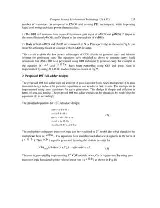
2 Proposed 12T full adder design
The proposed 12T full adder design incorporates the 3T XOR module made by tri-state inverter
as shown in Fig.7. The design follows with the conventional 2 module implementation of 3 input
XOR gate, this facilitate sum module of the full adder.
The modified equations (1) for 12T full adder design are:
cbaab
cabbacab
cabbcaabcab
bbacaabcabcabcab
cabcabcarry
cba
cbasum
)(
`)`()1(
``
`)(`)(
)(
⊕+⇒
+++⇒
+++⇒
++++=++
++=
⊕⊕⇒
⊕⊕=
(1)
The sum is generated by implementing 3T XOR module twice. Carry module is generated here by
using GDI technique.
The GDI approach allows implementation of a wide range of complex logic functions using only
two transistors. This method is suitable for design of fast, low-power circuits, using a reduced
5. Computer Science & Information Technology (CS & IT) 253
number of transistors (as compared to CMOS and existing PTL techniques), while improving
logic level swing and static power characteristics.
1) The GDI cell contains three inputs G (common gate input of nMOS and pMOS), P (input to
the source/drain of pMOS), and N (input to the source/drain of nMOS).
2) Body of both nMOS and pMOS are connected to N or P (respectively) as shown in Fig.8. , so
it can be arbitrarily biased at contrast with a CMOS inverter.
This circuit exploits the low power advantages of GDI circuits to generate carry and tri-state
inverter for generating sum. The equations have modified as above to generate carry. Basic
operations like AND, OR have performed using GDI technique to generate carry, for example in
the equation (1) ba. and cba )( ⊕ have been performed using GDI and gates. Sum is
implemented by using 3T (XOR) module twice as shown in Fig.9.
3 Proposed 10T full adder design:
The proposed 10T full adder uses the concept of pass transistor logic based multiplexer. The pass
transistor design reduces the parasitic capacitances and results in fast circuits. The multiplexer is
implemented using pass transistors for carry generation. This design is simple and efficient in
terms of area and timing. The proposed 10T full adder circuit can be visualised by modifying the
equations (2) as accordingly
The modified equations for 10T full adder design:
cbabaab
cbaab
cabcabcarry
cba
cbasum
)()`(
)(
)(
⊕+⊕⇒
⊕+⇒
++=
⊕⊕⇒
⊕⊕=
(2)
The multiplexer using pass transistor logic can be visualised in 2T model, the select signal for the
multiplexer here is ( ba ⊕ ). The equations have modified such that select signal is in the form of
( ba ⊕ ). The ( ba . ) signal is generated by using the tri-state inverter for
)`( ba => babbbabbabba .`..`).()``( ⇒+⇒+= (3)
The sum is generated by implementing 3T XOR module twice. Carry is generated by using pass
transistor logic based multiplexer whose select line is ( ba ⊕ ) as shown in Fig.10.
6. 254 Computer Science & Information Technology (CS & IT)
AB
CBA )( ⊕
Fig. .9. proposed 12T full adder design
AB
BA⊕
Fig. 10. proposed 10T full adder design
4 Proposed 8T full adder design:
In the proposed 8T full adder sum is generated using 3T XOR module twice, and carry is
generated using NMOS and PMOS pass transistor logic devices as shown in Fig.11. The
equations (4) are modified so as to visualise the 8T full adder design.
The modified equations for 8T full adder design are:
cbabba
cbaab
bbacaabcab
cabcabcarry
cba
cbasum
)()``(
)(
`)(`)(
)(
⊕+⇒
⊕+⇒
++++⇒
++=
⊕⊕⇒
⊕⊕=
(4)
In this design instead of using two NMOS pass transistor devices we have used one NMOS and
one PMOS pass transistor device, because of ease of the design and as according to the equation
as shown in Fig.11.
It must be noted that PMOS transistor passes ' l' very good, but cannot pass '0' completely thus,
the carry output has weak '0'. NMOS transistor passes '0' very good, but cannot pass '1'
completely therefore, the carry output has weak ' 1 ', Having weak '0' and '1' at carry outputs is
one of the disadvantages of proposed 8T full adder circuit. In practical situations, this problem
can be solved by using an inverter at carry output, but this solution leads to increased power and
area.
7. Computer Science & Information Technology (CS & IT) 255
BA`
BA⊕
Fig 11. Proposed 8T full adder design
4. SIMULATION RESULTS AND COMPARISON
The entire simulations have been done on 180nm single n-well CMOS bulk technology, in
virtuoso platform of cadence tool with the supply voltage 1.8V and frequency of 100MHz. The
entire results are compared with the different techniques. Area is calculated by using micro wind
software. The area is reduced by 48% for proposed 12T design, the area is reduced by 66% for
proposed 8T design and area is reduced by 53% when compared to 28T conventional full adder
design.
Table 1 Simulation Results
Full Adder
Designs
Convention
al(28T)
Chowdury
deign(8T)
8T(ref
.15)
8T(ref
.16)
SERF Proposed
(12T)
Proposed
(8T)
Proposed
(10T)
Min supply
voltage(V)
1.8 1.8 1.8 1.6 1.6 1.6 1.6 1.4
Cout delay
(nS)
0.366 0.513 0.496 0.5 0.39 0.476 0.502 0.512
Avg.power
consumptio
n (uW)
52.4 17.4 36.47 27.7 18.2 14.3 16.0 17.1
Number-of
transistors
28 8 8 8 10 12 8 10
Power*
Delay
(uW.nS) 19.178 8.926 18.08 12.6 7.09 6.806 8.032 8.755
5. CONCLUSION
Three new full adder designs have been proposed and simulation results have been compared
with the previous results in umc180nm technology using cadence tool. According to the
8. 256 Computer Science & Information Technology (CS & IT)
simulation results the power consumption has been improved maximum by 73% when proposed
circuits are compared to conventional 28T adder and other reference circuits.
Fig. .12. Simulation results and power waveform of Proposed 8T full adder
Fig. .13. Simulation results and power waveform of Proposed 10T full adder design
Fig. .14. Simulation results and power waveform of Proposed 12T full adder design
9. Computer Science & Information Technology (CS & IT) 257
REFERENCES
[1] Fayed and M. A. Bayoumi, “A low-power 10 transistor full adder cell for embedded architectures,” in
Proc. IEEE Int. Symp. Circuits Syst., 2001, pp.226–229.
[2] H. T. Bui, Y. Wang, and Y. Jiang, “Design and analysis of low-power 10-transistor full adders
using XOR XNOR gates,” IEEE Trans. Circuits Syst. II, Analog and Digi-tal Signal Processing.,
vol.49, no. 1, pp. 25–30, Jan. 2002.
[3] J.-F. Lin, Y.-T. Hwang, M.-H. Sheu and C.-C. Ho, “A novel high speed and energy efficient 10-
transistor full adder design,” IEEE Trans. Circuits Syst. I, vol. 54, no. 5, pp. 1050–1059, May 2007.
[4] Y. Jiang, Al-Sheraidah. A, Y. Wang, Sha. E, and J. G. Chung, “A novel multiplexer-based low-power
full adder,” IEEE Trans. Circuits Syst. II, Analog Digit. Signal Process., vol. 51, pp.345–348, July
2004.
[5] Dan Wang, Maofeng Yang, Wu Cheng XUguang Guan, Zhangming Zhu, Yintang Yang “ Novel Low
power Full Adder Cells in 180nm CMOS Technology”, 4th IEEE conference on Industrial Electronics
and Applications, pp. 430-433,2009.
[6] Sreehari Veeramachaneni, M.B. Srinivas, "New improved I•bit full adder cells ", Ca-nadian
Conference on Electrical and Computer Engineering, pp. 000735 -000738, 2008.
[7] Chuen•Yau, Chen and, Yung•Pei Chou, "Novel Low•Power I•bit Full Adder Design", 9th
International Symposium on Communications and Information Technology, pp. 1348 -1349, 2009
[8] F.Moradi, DTWisland, H.Mahmoodi, S.Aunet; T.V.Cao, A.Peiravi, "Ultra low power full adder
topologies", IEEE International Symposium on Circuits and Systems, pp. 3158-3161, 2009.
[9] Amir Ali Khatibzadeh, Kaamran Raahemifar, "A 14•TRANSISTOR LOW POWER HIGH•SPEED
FULL ADDER CELL", Canadian Conference on Electrical and Com-puter Engineering, vol. I, pp.
163-166, 2003.
[10] AK. Singh, C.M.R. Prabhu, K.M.Almadhagi, S.F. Farea, K. Shaban,"A Proposed 10•T Full Adder
Cell for Low Power Consumption", International Conference on Electrical Engineering/Electronics
Computer Telecommunications and Information Technology (ECTI•CON), pp. 389 -391, 2010.
[11] IIham Hassoune, Denis Flandre, .Iean•Didier Legat," ULPF A: A New Efficient De-sign of a Power•
Aware Full Adder", IEEE Transactions on Circuits and Systems I: Regular Papers, Vol. 57, pp. 2066 -
2074, August 2010.
[12] S. Goel, A. Kumar, and M. A. Bayoumi, “Design of robust, energy-efficient full ad-ders for deep
submicrometer design using hybrid-CMOS logic style,” IEEE Trans. Very Large Scale Integr. (VLSI)
Syst., vol. 14, no. 12, pp.1309–1321, Dec. 2006.
[13] H. T. Bui, Y. Wang, and Y. Jiang, “Design and analysis of low-power 10-transistor full adders using
XOR–XNOR gates,” IEEE Trans. Circuits Syst. II, Analog Digit. Signal Process., vol. 49, no. 1, pp.
25–30, Jan. 2002.
[14] J.-F. Lin, Y.-T. Hwang, M.-H. Sheu and C.-C. Ho, “A novel high speed and energy efficient 10-
transistor full adder design,” IEEE Trans. Circuits Syst. I, vol. 54, no. 5, pp. 1050–1059, May 2007.
[15] Yi WEI, Ji-zhong SHEN, “Design of a novel low power 8-transistor 1-bit full adder cell”, Journal of
Zhejiang University-SCIENCE C (Computers & Electronics), vol. 7,pp 504-507, Dec 2011.
[16] Nabiallah Shiri Asmangerdi, Javad Forounchi and Kuresh Ghanbari, “A new 8- Transistor Floating
Full-Adder Circuit”, IEEE Trans. 20th Iranian Conference on Electrical Engineering, (ICEE2012),
pp. 1405-1409, May, 2012.