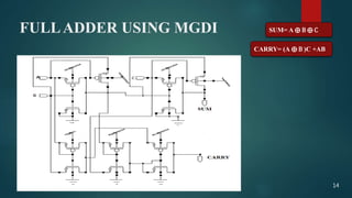
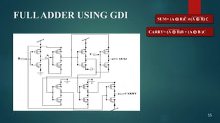
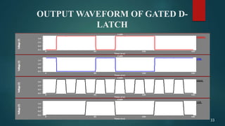
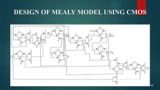
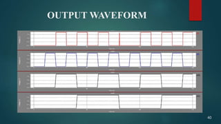
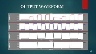
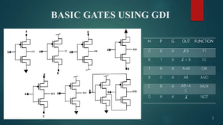
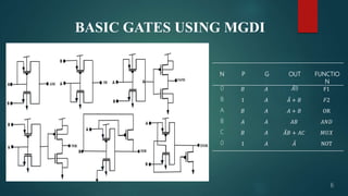
The document describes a study and performance analysis of the Modified Gate Diffusion Input (MGDI) technique. It provides details on MGDI logic, including how it overcomes limitations of the Gate Diffusion Input (GDI) technique. Various logic gates and circuits like full adders, flip-flops, and finite state machines are designed using MGDI. Simulation results show that MGDI outperforms GDI and traditional CMOS logic in terms of transistor count, power dissipation, and delay. While self-resetting logic has higher transistor count and power, it provides an alternative to dynamic logic by removing the need for a global clock.


![Literature review
A new low power design technique, GDI has been
introduced. This technique allows implementation of a
wide range of complex logic function using only two
transistor which makes this suitable for design of fast low
power circuit, using a reduced number of transistor while
improving static power characteristics and allowing
simple top down design by using small cell library.[1]
Arkaidy Morgenshtein et
al. (2002)
Massimo Alioto et al.
(2003)
Another technique for high speed low power circuit was implemented which was
based on mixing different logic styles to implement arithmetic circuit. Here fast full
adders chains without driving capability interrupted by full adders with driving
capability are considered and optimized for minimum delay.[2]
8](https://image.slidesharecdn.com/shubhamjha-copy2-180719064335/85/Modified-Gate-Diffusion-Input-MGDI-10-320.jpg)
![D-FF was implemented by using GDI technique [1]. Performance comparison with
other D-FF design was done with respect to gate area, delay and power dissipation and
the proposed structures showed upto 45% reduction in PDP and the reduction in gate
area.[3]
Arkaidy Morgenshtein et
al. (2004)
Massimo Alioto et al.
(2007)
Adder was designed using mixed topology [2] and compared it with single topology
for technology spanning five technology nodes( from 90 nm to 0.35 um). Results show
that the mixed topology is very efficient over single topology and its advantage
increases as down-scaling the technology.[4]
Based on mixed topology full adder based on mixed GDI has been designed. As
compared to the previous [1] here GDI full adders are followed by inverters in the
long full adder chains to alleviate the problem of signal degradation during
propagation through long chain.[5]
Adarsh Kumar Agarwal
et al. (2009)
9](https://image.slidesharecdn.com/shubhamjha-copy2-180719064335/85/Modified-Gate-Diffusion-Input-MGDI-11-320.jpg)
![4-Bit full adder was designed using SRL, here SRL is compared with dynamic logic at
gate level and performance comparison.Dynamic logic lacks in the application of
clock distribution grid and routing to dynamic gates that presents a problem to CAD
tools and introduces issues of delay and skew into the circuit design process, this is
solved by SRL. The only deficit is that it occupies more Si area.[6]
R. Uma (2011)
R. Uma et al. (2012)
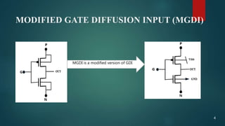
Modified-GDI is introduced , earlier GDI can be fabricated only in twin well CMOS
process or SOI process to realize a chip, this increases the complexity as well as the
cost of fabrication. But MGDI can be fabricated in any standard CMOS fabrication
process.[7]
Here the nMOS block of conventional SRL[6] is replaced by the Mod-GDI block.
This structure reduces the transistor count and dynamic power dissipation. In
conventional CMOS the upper pMOS and the lower nMOS stack is connected to VDD
and GND , which provides a low impedance path between VDD and gnd. This situation
is eliminated in this logic. So by combining SRL and MGDI the circuit produces high
speed and low power output.[8]
R. Uma et al. (2012)
10](https://image.slidesharecdn.com/shubhamjha-copy2-180719064335/85/Modified-Gate-Diffusion-Input-MGDI-12-320.jpg)
![Three low power full adders are designed with full swing AND, OR and XOR gates
to alleviate threshold voltage problem which is commonly encountered in Gate Diffusion
Input (GDI) logic. The enhanced driving capability also facilitates lower voltage and
faster operation which leads to less energy consumption. The performance of the
proposed designs is compared with the other full adder designs, namely CMOS, CPL,
hybrid and GDI through SPICE simulations using 45 nm technology models.[10]
Mrs. K.Kalaiselvi et al.
(2014)
Mohan Shoba et al.
(2016)
In the proposed paper the adder circuits is designed in Self resetting logic and the
number of transistors in the modified design is reduced. The goal is to obtain a family
of adders that could simplify the implementation of fast processing circuit which
overcomes the restriction due to the pulses being elongated and shortened as signal
traverse the logic stages. The circuits are designed in 120nm processing CMOS
processing technology. [9]
R. Uma et al.
(2017)
Design of low power adder is done using SRLGDI.In the proposed design structure , the
pull down tree is implemented with (GDI) with level restoration which apparently
eliminates the conductance overlap between nMOS and pMOS devices which was
encountered in the case of conventional SRL [6], thereby reducing the short circuit
power dissipation and providing High Output Voltage.[11]
11](https://image.slidesharecdn.com/shubhamjha-copy2-180719064335/85/Modified-Gate-Diffusion-Input-MGDI-13-320.jpg)