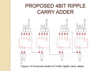
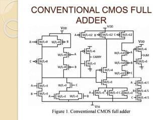
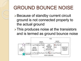
4-BIT CMOS FULLADDER IN SUB
MICRON TECHNOLOGY FOR LOW
LEAKAGE AND GROUND BOUNCE NOISE
REDUCTION
PROJECT GUIDE :
Mr. Y.CHANDRA SEKHAR
ASSOCIATE PROFESSOR
BY:
P.AYYAPPA (11QNIAO401)
P.SHIREESHA(11QN1A0454)
M.MAHESH (11QN1A0405)
G.BHARATH (11QN1A0446)
INTRODUCTION
 For complex arithmetic circuits,
Ground bounce noise is given an
equal importance like leakage current,
active power, delay and area.
 Reduction of leakage power and
ground bounce noise reduction using
sleep transistor in 4 bit CMOS full
adder implementation
WHY ONLY MOSFET ?
BJT:
In NPN current conduction occurs by
majority and minority charge carriers
Cannot withstand high temperature
Leakage current will be dissipated
because of minority charge carriers
CMOS LOGIC STYLE
 CMOS=PMOS+NMOS

COMBINATIONAL CIRCUIT
FOR FULL ADDER
FULL ADDER
BOOLEN EXPRESSIONS FOR
FULL ADDER
 CARRY=AB+BC+AC
 SUM =A B C
REDUCED FORM:
CARRY: AB+C(A+B)
________
SUM:AB+C(A+B) (A+B+C)+ABC
+
+
+
4-BIT FULL ADDER
For adding any bits of input we require
as many number of full adders
In this paper we are adding 4 bits of
input
Four full adders can be taken in the form
of “Ripple Carry Adder”
The generated carry is rippled to next full
adder
PROPOSED 4BIT RIPPLE
CARRY ADDER
POWER CONSUMPTION IN
CMOS
LEAKAGE POWER
 The partial power dissipation at sub
threshold region where the voltage is
less than vth(0<v<0.7)
P LEAKAGE = VDD ILEAKAGE
POWER DISSIPATION IN
CMOS
Ptotal (0→1) = CL VDD
2 +tscVDD Ipeak
+VDDIleakage
%75 %5%20
CL
VDD VDD
REASONS FOR LEAKAGE
POWER
Power loss at sub threshold region
REASONS FOR LEAKAGE
POWER
Dissipation because of short circuit
formed between V dd and ground
Gate tunneling current
REASONS FOR LEAKAGE
POWER
 Formation of parasitic capacitors
REDUCTION OF POWER
CONSUMPTION IN CMOS
Power gating
technique
Sleep transistor
POWER GATING
TECHNIQUE
A flip-flop along with adder is used
Flip-flop is a sequential circuit and its o/p
depends on present i/p and past o/p
The carry and sum circuits are divided
into separate blocks and are cascaded
Size of the transistor can be reduced by
changing the W/L ratio with appropriate
values
CONVENTIONAL CMOS FULL
ADDER
POWER GATING-MERITS
Sub threshold current is directly
proportional to width/length ratio of
transistor
This sizing reduces the standby leakage
current(sub threshold current)
Reduces the area occupied by the circuit
and silicon chip
Reduction in cost
GROUND BOUNCE NOISE
Because of standby current circuit
ground is not connected properly to
the actual ground
This produces noise at the transistors
and is termed as ground bounce noise
REDUCTION OF GROUND
BOUNCE NOISE
For further modified design of the
circuit the amount of noise at the
ground will be more
We use sleep transistors to reduce the
ground bounce noise
FULL ADDER WITH SLEEP
CIRCUIT
DESIGN:1 DESIGN:2
COMPARISON
 Modified adder circuit of Design 2
shown in Figure 3
 W /L ratio of PMOS is 1.5 times
that of W /L ratio of NMOS
 each block has been treated as
an equivalent inverter
 Further compared to the Base
case, Design 1 and Design 2,
ground bounce noise produced
 It is reduced by sleep transistor
IMPROVED GROUND BOUNCE
NOISE REDUCTION
EXPLANATION
control transistor is connected b/w gate
and source
When i/p is fed to the control transistor,
a short circuit is formed
 The sleep transistor acts as a diode
charge stored in the carry block is
discharged through ST-1
 Same signals are applied to sum
generation part also but with duration
of half of the oscillation period.
 Noise cancellation occurs once the
second sleep transistor (ST2) turns
on due to phase shift between the
noise induced by the second sleep
transistor
H-SPICE:

4 bit cmos full adder in submicron technology with low leakage and ground bounce noise reduction

  • 1.
    4-BIT CMOS FULLADDERIN SUB MICRON TECHNOLOGY FOR LOW LEAKAGE AND GROUND BOUNCE NOISE REDUCTION PROJECT GUIDE : Mr. Y.CHANDRA SEKHAR ASSOCIATE PROFESSOR BY: P.AYYAPPA (11QNIAO401) P.SHIREESHA(11QN1A0454) M.MAHESH (11QN1A0405) G.BHARATH (11QN1A0446)
  • 2.
    INTRODUCTION  For complexarithmetic circuits, Ground bounce noise is given an equal importance like leakage current, active power, delay and area.  Reduction of leakage power and ground bounce noise reduction using sleep transistor in 4 bit CMOS full adder implementation
  • 3.
    WHY ONLY MOSFET? BJT: In NPN current conduction occurs by majority and minority charge carriers Cannot withstand high temperature Leakage current will be dissipated because of minority charge carriers
  • 4.
    CMOS LOGIC STYLE CMOS=PMOS+NMOS 
  • 5.
  • 6.
  • 7.
    BOOLEN EXPRESSIONS FOR FULLADDER  CARRY=AB+BC+AC  SUM =A B C REDUCED FORM: CARRY: AB+C(A+B) ________ SUM:AB+C(A+B) (A+B+C)+ABC + + +
  • 8.
    4-BIT FULL ADDER Foradding any bits of input we require as many number of full adders In this paper we are adding 4 bits of input Four full adders can be taken in the form of “Ripple Carry Adder” The generated carry is rippled to next full adder
  • 9.
  • 10.
  • 12.
    LEAKAGE POWER  Thepartial power dissipation at sub threshold region where the voltage is less than vth(0<v<0.7) P LEAKAGE = VDD ILEAKAGE
  • 13.
    POWER DISSIPATION IN CMOS Ptotal(0→1) = CL VDD 2 +tscVDD Ipeak +VDDIleakage %75 %5%20 CL VDD VDD
  • 14.
    REASONS FOR LEAKAGE POWER Powerloss at sub threshold region
  • 15.
    REASONS FOR LEAKAGE POWER Dissipationbecause of short circuit formed between V dd and ground Gate tunneling current
  • 16.
    REASONS FOR LEAKAGE POWER Formation of parasitic capacitors
  • 17.
    REDUCTION OF POWER CONSUMPTIONIN CMOS Power gating technique Sleep transistor
  • 18.
    POWER GATING TECHNIQUE A flip-flopalong with adder is used Flip-flop is a sequential circuit and its o/p depends on present i/p and past o/p The carry and sum circuits are divided into separate blocks and are cascaded Size of the transistor can be reduced by changing the W/L ratio with appropriate values
  • 19.
  • 20.
    POWER GATING-MERITS Sub thresholdcurrent is directly proportional to width/length ratio of transistor This sizing reduces the standby leakage current(sub threshold current) Reduces the area occupied by the circuit and silicon chip Reduction in cost
  • 21.
    GROUND BOUNCE NOISE Becauseof standby current circuit ground is not connected properly to the actual ground This produces noise at the transistors and is termed as ground bounce noise
  • 22.
    REDUCTION OF GROUND BOUNCENOISE For further modified design of the circuit the amount of noise at the ground will be more We use sleep transistors to reduce the ground bounce noise
  • 23.
    FULL ADDER WITHSLEEP CIRCUIT DESIGN:1 DESIGN:2
  • 24.
    COMPARISON  Modified addercircuit of Design 2 shown in Figure 3  W /L ratio of PMOS is 1.5 times that of W /L ratio of NMOS  each block has been treated as an equivalent inverter  Further compared to the Base case, Design 1 and Design 2, ground bounce noise produced  It is reduced by sleep transistor
  • 25.
  • 26.
    EXPLANATION control transistor isconnected b/w gate and source When i/p is fed to the control transistor, a short circuit is formed  The sleep transistor acts as a diode charge stored in the carry block is discharged through ST-1
  • 27.
     Same signalsare applied to sum generation part also but with duration of half of the oscillation period.  Noise cancellation occurs once the second sleep transistor (ST2) turns on due to phase shift between the noise induced by the second sleep transistor
  • 28.