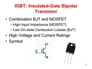
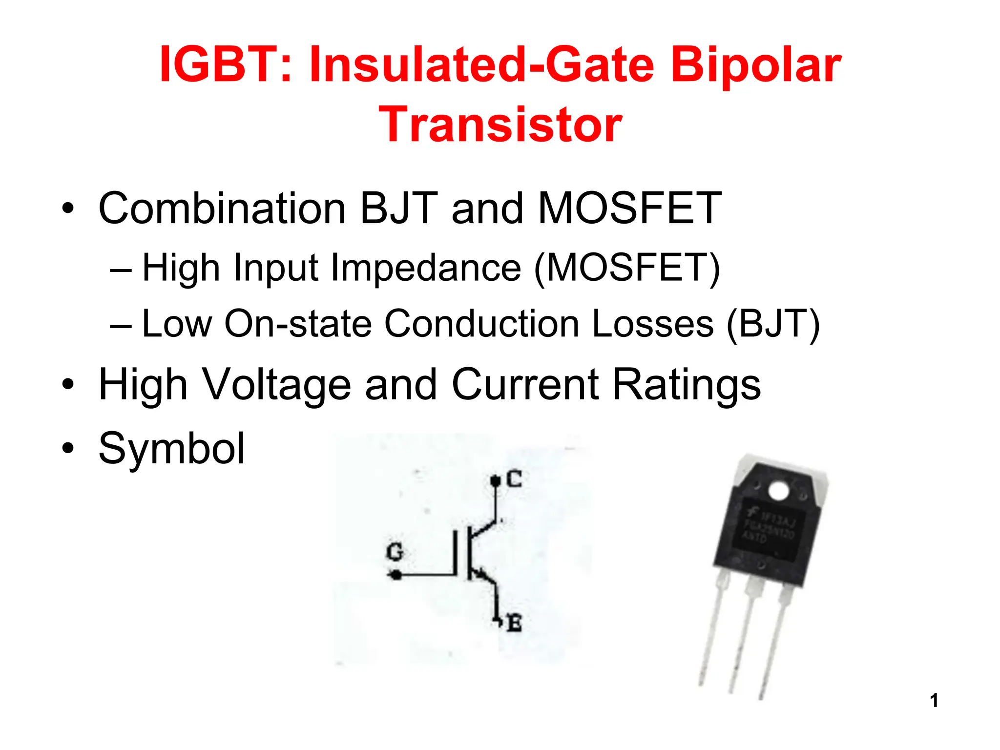
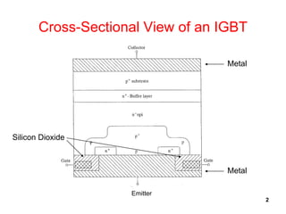
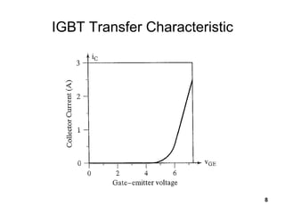
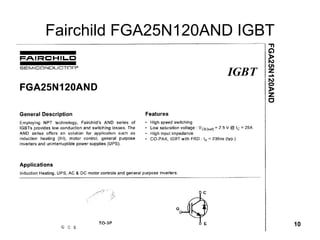
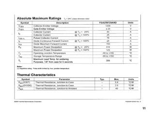
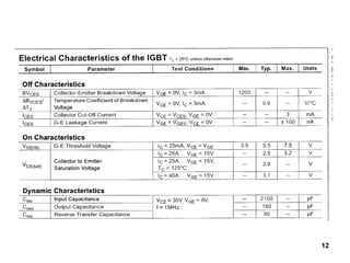
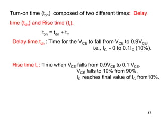
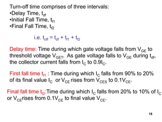
1. 1
IGBT: Insulated-Gate Bipolar
Transistor
• Combination BJT and MOSFET
– High Input Impedance (MOSFET)
– Low On-state Conduction Losses (BJT)
• High Voltage and Current Ratings
• Symbol
3. 3
IGBT Equivalent Circuit for VGE<VT
+
VCC
IEPNP
ICPNP
IBPNP
ICNPN
IENPN
IBNPN
Leakage Current
IRBE
Both transistors are OFF
4. 4
IGBT Equivalent Circuit for VGE>VT
+
VCC
NPN Transistor
becomes forward
biased at the BE,
drawing current
from the Base of
the PNP transistor.
MOS transistor conducts,
drawing current from the
Base of the PNP transistor.
PNP transistor turns ON,
RMOD decreases due to
carrier injection from the
PNP Emitter.
9. 9
Example of IGBT Ratings
• Used in high voltage / current & high frequency
switching power applications (Inverters, SMPS).
• Example: IGBT 2500V / 2400A.
• Max. Frequency: 20KHz.
• Switching time: 5 to sec.
• On state resistance: 2.3m.
9
17. 17
Turn-on time (ton) composed of two different times: Delay
time (tdn) and Rise time (tr).
ton = tdn + tr.
Delay time tdn : Time for the VCE to fall from VCE to 0.9VCE.
i.e., IC - 0 to 0.1IC (10%).
Rise time tr : Time when VCE falls from 0.9VCE to 0.1 VCE.
VCE falls to 10% from 90%.
IC reaches final value of IC from10%.
18. 18
Turn-off time comprises of three intervals:
•Delay Time, tdf
•Initial Fall Time, tf1
•Final Fall Time, tf2
i.e. toff = tdf + tf1 + tf2
Delay time: Time during which gate voltage falls from VGE to
threshold voltage VGET. As gate voltage falls to VGE during tdf,
the collector current falls from IC to 0.9IC.
First fall time tf1 : Time during which IC falls from 90% to 20%
of its final value IC or VCE rises from VCES to 0.1VCE.
Final fall time tf2:Time during which IC falls from 20% to 10% of IC
or VCErises from 0.1VCE to final value VCE.
19. Design of Gate Driver circuits
• Power electronics applications employ power device
switches.
• Every switch needs a driver – the right driver makes a
difference.
• Gate drivers provide a wide range of typical output current
options, from 0.1-A up to 10-A.
• Robust gate drive protection features such as fast short-
circuit protection, active Miller clamp, shoot-through
protection, fault, shutdown, and over current protection
19
20. Gate driver ICs
• Gate driver ICs serve as the interface between control
signals (digital or analog controllers) and power switches
(IGBTs, MOSFETs, SiC MOSFETs, and GaNHEMTs).
• The integrated gate driver solutions reduce our design
complexity, development time, bill of materials (BOM),
and board space while improving reliability over
discretely-implemented gate-drive solutions.
• Gate driver ICs with a variety of configurations, voltage
classes, isolation levels, protection features, and
package options.
20
21. Gate driver IC Selection
By
• Configuration
• Isolation
• Application
• Switch device
21
22. Configuration
• High side
• Low side
• High and Low side
• Half bridge
• Full Bridge
• Three phase
• Driver boards
• Gate driver support Ics
• Synchronous buck 22