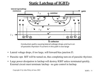
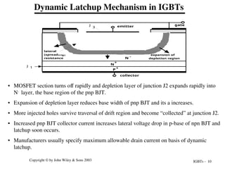
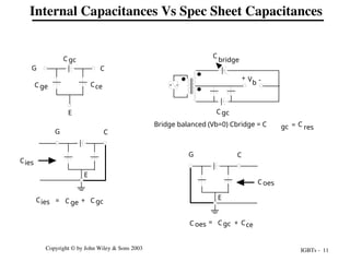
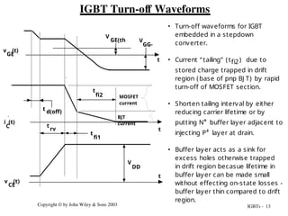
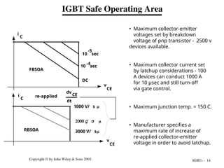
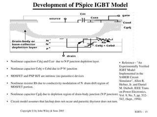
IGBTs - 1
Copyright © by John Wiley & Sons 2003
Insulated Gate Bipolar Transistors (IGBTs)
Lecture Notes
Outline
• Construction and I-V characteristics
• Physical operation
• Switching characteristics
• Limitations and safe operating area
• PSPICE simulation models
IGBTs - 2
Copyright © by John Wiley & Sons 2003
Multi-cell Structure of IGBT
• IGBT = insulated gate bipolar transistor.
N +
N
+
N
+ N +
N -
N+
P
P
gate
oxide
gate
conductor
field
oxide
emitter
conductor
contact to source
diffusion
gate
width
P
+
collector
metallization
buffer layer
(not essential)
IGBTs - 3
Copyright © by John Wiley & Sons 2003
Cross-section of IGBT Cell
• Cell structure similar to power MOSFET (VDMOS) cell.
• P-region at collector end unique feature of IGBT compared to MOSFET.
• Punch-through (PT) IGBT - N+
buffer layer present.
• Non-punch-through (NPT) IGBT - N+
buffer layer absent.
P
+
N
-
N
+
P
N
+
N
+
emitter
gate
collector
SiO
2
J
2
J
3
Ls
Parasitic thyristor
Buffer layer
(not essential)
J
1
- Unique feature of IGBT
IGBTs - 4
Copyright © by John Wiley & Sons 2003
N+
N-
P P
N+ N+
Collector
Emitter
Gate
conductor
Oxide
Parasitic
SCR
Channel
length
boddy-source short
I
D
I
D
P
+
Cross-section of Trench-Gate IGBT Unit Cell
N-
P P
N+ N+
Collector
Emitter
Gate
conductor
Oxide
Parasitic
SCR
Channel
length
boddy-source short
ID
I
D
P
+
• Non-punch-thru IGBT
• Punch-thru IGBT
IGBTs - 5
Copyright © by John Wiley & Sons 2003
collector
emitter
gate
gate
drain
source
IGBT I-V Characteristics and Circuit Symbols
• Transfer curve
• Output characteristics
• N-channel IGBT circuit symbols
i
C
v
CE
BV
CES
V
RM
increasing V
GE
• No Buffer Layer
VRM BV
≈
CES
• With Buffer Layer
V
RM
0
≈
GE3
v
GE1
v
GE2
v
GE4
v
i
C
v
GE
V
GE(th)
IGBTs - 6
Copyright © by John Wiley & Sons 2003
Blocking (Off) State Operation of IGBT
• With N+ buffer layer, junction J 1 has
small breakdownvoltage and thus IGBT
has little reverse blocking capability -
anti-symmetric IGBT
• Buffer layer speeds up device turn-off
• Blocking state operation - VGE < VGE(th)
• J unction J 2 is blocking junction - n+ drift
region holds depletion layer of blocking
junct ion.
• Without N+ buffer layer, IGBT has large
reverse blocking c apability - s o-called
symmetric IGBT
P+
N -
N
+
P
N
+
N
+
emitter
gate
collector
SiO
2
J
2
J
3
L s
Parasitic thyristor
Buffer layer
(not essential)
J
1
- Unique feature of IGBT
IGBTs - 7
Copyright © by John Wiley & Sons 2003
IGBT On-state Operation
P
+
N
-
N
+
P
N
+
N
+
emitter
gate
collector
lateral (spreading)
resistance
+
+ +
+ +
+ +
+
P+
N
-
N
+
P
N
+
N
+
collector
emitter
gate
• MOSFET se ction designed
to carry most of t he IGBT
collector current
• On-state VCE(on) =
VJ 1 + V drift + ICRchannel
• Hole injection into drift
region from J 1 minimizes
Vdrift.
IGBTs - 8
Copyright © by John Wiley & Sons 2003
• Approximate equivalent circuit for
IGBT valid for normal operating
conditions.
• IGBT equivalent circuit showing
transistors comprising the parasitic
thyristor.
Approximate Equivalent Circuits for IGBTs
gate
collector
emitter
Body region
spreading
resistance
Principal
(desired)
path of
collector
current
Conduction path resulting
in thyristor turn-on (IGBT
latchup) if current in this
path is too large
gate
drift region
resistance
V
J1
V
drift
I R
C channel
• VCE(on) = V J 1 + Vdrift + IC Rchannel
IGBTs - 9
Copyright © by John Wiley & Sons 2003
• Lateral voltage drops, if too large, will forward bias junction J3.
• Parasitic npn BJT will be turned on, thus completing turn-on of parasitic thyristor.
• Large power dissipation in latchup will destroy IGBT unless terminated quickly.
External circuit must terminate latchup - no gate control in latchup.
Static Latchup of IGBTs
P+
N -
N
+
P
N
+
N
+
emitter
gate
collector
lateral (spreading)
resistance
+
+
Conduction paths causing lateral voltage drops and turn-on
of parasitic thyristor if current in this path is too large
+ + + + +
J 1
2
J
3
J
IGBTs - 10
Copyright © by John Wiley & Sons 2003
Dynamic Latchup Mechanism in IGBTs
• MOSFET section turns off rapidly and depletion layer of junction J2 expands rapidly into
N-
layer, the base region of the pnp BJT.
• Expansion of depletion layer reduces base width of pnp BJT and its a increases.
• More injected holes survive traversal of drift region and become “collected” at junction J2.
• Increased pnp BJT collector current increases lateral voltage drop in p-base of npn BJT and
latchup soon occurs.
• Manufacturers usually specify maximum allowable drain current on basis of dynamic
latchup.
P+
N -
N
+
P
N
+
N
+
emitter gate
collector
lateral
(spreading)
resistance
J 1
2
J
3
J
expansion of
depletion region
IGBTs - 11
Copyright © by John Wiley & Sons 2003
Internal Capacitances Vs Spec Sheet Capacitances
G C
E
C gc
ge
C ce
C
ies
C
G C
E
ies
C = ge
C + C gc
oes
C
G C
E
C gc ce
C
oes
C = +
C gc
C
bridge
+ -
V
b
res
C
Bridge balanced (Vb=0) Cbridge = C =
gc
IGBTs - 12
Copyright © by John Wiley & Sons 2003
IGBT Turn-on Waveforms
V
GG+
I o
v (t)
GE
i (t)
C
V
DD
v (t)
CE
V
CE (on)
t
d(on)
t
ri
t
fv1
t
t
t
tfv2
• Turn-on waveforms for
IGBT embedded in a
stepdown converter.
• Ve ry similar to turn-on
waveforms of MOSFETs.
• Contributions to tvf2.
• Increase in Cge of
MOSFET se ction at low
collector-emitter
voltages.
• Slower turn-on of pnp
BJT section.
IGBTs - 13
Copyright © by John Wiley & Sons 2003
IGBT Turn-off Waveforms
• Turn-off waveforms for IGBT
embedded in a stepdown
converter.
• Current “tailing” (tfi2) due to
stored charge trapped in drift
region (base of pnp BJ T) by rapid
turn-off of MOSFET section.
• Shorten tailing interval by either
reducing carrier lifetime or by
putting N+ buffer layer adjacent to
injecting P+ layer at drain.
• Buffer layer acts as a sink for
excess holes otherwise trapped
in drift region becasue lifetime in
buffer layer can be made small
without effecting on-state losses -
buffer layer thin compared to drift
region.
V
GG-
v (t)
GE
i (t)
C
V
DD
v (t)
CE
t d(off)
t
rv
t
fi1
t
t
t
t
fi2
V
GE(th
)
MOSFET
current
BJT
current
IGBTs - 14
Copyright © by John Wiley & Sons 2003
IGBT Safe Operating Area
i
C
v
CE
10 sec
-5
10 sec
-4
DC
1000 V/ s μ
2000 V/ s μ
μ
3000 V/ s
re-applied
dv
CE
dt
FBSOA
RBSOA
i
C
v
CE
• Maximum collector-emitter
voltages set by breakdown
voltage of pnp transistor - 2500 v
devices available.
• Maximum collector current set
by latchup considerations - 100
A devices can conduct 1000 A
for 10 µsec and still turn-off
via gate control.
• Maximum junction temp. = 150 C.
• Manufacturer specifies a
maximum rate of increase of
re-applied collector-emitter
voltage in order to avoid latchup.
IGBTs - 15
Copyright © by John Wiley & Sons 2003
Development of PSpice IGBT Model
P
+
N
-
N
+
P
N
+
N
+
drain
source
gate
Coxd
Cgdj
Cdsj
Ccer
Coxs
Cm
Cebj + Cebd
Drain-body or
base-collector
depletion layer
Rb
• Reference - "An
Experimentally Verified
IGBT Model
Implemented in the
SABER Circuit
Simulator", Allen R.
Hefner, Jr. and Daniel
M. Diebolt, IEEE Trans.
on Power Electronics,
Vol. 9, No. 5, pp. 532-
542, (Sept., 1994)
• Nonlinear capacitors Cdsj and Ccer due to N-
P junction depletion layer.
• Nonlinear capacitor Cebj + Cebd due to P+
N+
junction
• MOSFET and PNP BJT are intrinsic (no parasitics) devices
• Nonlinear resistor Rb due to conductivity modulation of N-
drain drift region of
MOSFET portion.
• Nonlinear capacitor Cgdj due to depletion region of drain-body junction (N-
P junction).
• Circuit model assumes that latchup does not occur and parasitic thyristor does not turn.
IGBTs - 16
Copyright © by John Wiley & Sons 2003
Parameter Estimation for PSpice IGBT Model
• Built-in IGBT model requires nine parameter values.
• Parameters described in Help files of Parts utility program.
• Parts utility program guides users through parameter estimation process.
• IGBT specification sheets provided by manufacturer provide sufficient
informaiton for general purpose simulations.
• Detailed accurate simulations, for example device dissipation studies, may
require the user to carefully characterize the selected IGBTs.
Cm +
Coxs
Cgdj
Coxd
Cdsj
Rb
Cebj +
Cebd
Ccer
Drain
Source
Gate
• Built-in model does not model
ultrafast IGBTs with buffer
layers (punch-through IGBTs) or
reverse free-wheeling diodes
IGBTs - 17
Copyright © by John Wiley & Sons 2003
1
nF
0.75
nF
0.5
nF
0.25
nF
0
100 V 200 V 300 V 400 V 500 V
Collector - emitter Voltage
V = 0 V
GE
Simulated C versus V
for IXGH40N60
GC CE
0 V 5 V 10 V 15 V 20 V 25 V
Data from IXGH40N60 spec sheet
PSpice IGBT - Simulation Vs Experiment

IGBT(.........................................)

  • 1.
    IGBTs - 1 Copyright© by John Wiley & Sons 2003 Insulated Gate Bipolar Transistors (IGBTs) Lecture Notes Outline • Construction and I-V characteristics • Physical operation • Switching characteristics • Limitations and safe operating area • PSPICE simulation models
  • 2.
    IGBTs - 2 Copyright© by John Wiley & Sons 2003 Multi-cell Structure of IGBT • IGBT = insulated gate bipolar transistor. N + N + N + N + N - N+ P P gate oxide gate conductor field oxide emitter conductor contact to source diffusion gate width P + collector metallization buffer layer (not essential)
  • 3.
    IGBTs - 3 Copyright© by John Wiley & Sons 2003 Cross-section of IGBT Cell • Cell structure similar to power MOSFET (VDMOS) cell. • P-region at collector end unique feature of IGBT compared to MOSFET. • Punch-through (PT) IGBT - N+ buffer layer present. • Non-punch-through (NPT) IGBT - N+ buffer layer absent. P + N - N + P N + N + emitter gate collector SiO 2 J 2 J 3 Ls Parasitic thyristor Buffer layer (not essential) J 1 - Unique feature of IGBT
  • 4.
    IGBTs - 4 Copyright© by John Wiley & Sons 2003 N+ N- P P N+ N+ Collector Emitter Gate conductor Oxide Parasitic SCR Channel length boddy-source short I D I D P + Cross-section of Trench-Gate IGBT Unit Cell N- P P N+ N+ Collector Emitter Gate conductor Oxide Parasitic SCR Channel length boddy-source short ID I D P + • Non-punch-thru IGBT • Punch-thru IGBT
  • 5.
    IGBTs - 5 Copyright© by John Wiley & Sons 2003 collector emitter gate gate drain source IGBT I-V Characteristics and Circuit Symbols • Transfer curve • Output characteristics • N-channel IGBT circuit symbols i C v CE BV CES V RM increasing V GE • No Buffer Layer VRM BV ≈ CES • With Buffer Layer V RM 0 ≈ GE3 v GE1 v GE2 v GE4 v i C v GE V GE(th)
  • 6.
    IGBTs - 6 Copyright© by John Wiley & Sons 2003 Blocking (Off) State Operation of IGBT • With N+ buffer layer, junction J 1 has small breakdownvoltage and thus IGBT has little reverse blocking capability - anti-symmetric IGBT • Buffer layer speeds up device turn-off • Blocking state operation - VGE < VGE(th) • J unction J 2 is blocking junction - n+ drift region holds depletion layer of blocking junct ion. • Without N+ buffer layer, IGBT has large reverse blocking c apability - s o-called symmetric IGBT P+ N - N + P N + N + emitter gate collector SiO 2 J 2 J 3 L s Parasitic thyristor Buffer layer (not essential) J 1 - Unique feature of IGBT
  • 7.
    IGBTs - 7 Copyright© by John Wiley & Sons 2003 IGBT On-state Operation P + N - N + P N + N + emitter gate collector lateral (spreading) resistance + + + + + + + + P+ N - N + P N + N + collector emitter gate • MOSFET se ction designed to carry most of t he IGBT collector current • On-state VCE(on) = VJ 1 + V drift + ICRchannel • Hole injection into drift region from J 1 minimizes Vdrift.
  • 8.
    IGBTs - 8 Copyright© by John Wiley & Sons 2003 • Approximate equivalent circuit for IGBT valid for normal operating conditions. • IGBT equivalent circuit showing transistors comprising the parasitic thyristor. Approximate Equivalent Circuits for IGBTs gate collector emitter Body region spreading resistance Principal (desired) path of collector current Conduction path resulting in thyristor turn-on (IGBT latchup) if current in this path is too large gate drift region resistance V J1 V drift I R C channel • VCE(on) = V J 1 + Vdrift + IC Rchannel
  • 9.
    IGBTs - 9 Copyright© by John Wiley & Sons 2003 • Lateral voltage drops, if too large, will forward bias junction J3. • Parasitic npn BJT will be turned on, thus completing turn-on of parasitic thyristor. • Large power dissipation in latchup will destroy IGBT unless terminated quickly. External circuit must terminate latchup - no gate control in latchup. Static Latchup of IGBTs P+ N - N + P N + N + emitter gate collector lateral (spreading) resistance + + Conduction paths causing lateral voltage drops and turn-on of parasitic thyristor if current in this path is too large + + + + + J 1 2 J 3 J
  • 10.
    IGBTs - 10 Copyright© by John Wiley & Sons 2003 Dynamic Latchup Mechanism in IGBTs • MOSFET section turns off rapidly and depletion layer of junction J2 expands rapidly into N- layer, the base region of the pnp BJT. • Expansion of depletion layer reduces base width of pnp BJT and its a increases. • More injected holes survive traversal of drift region and become “collected” at junction J2. • Increased pnp BJT collector current increases lateral voltage drop in p-base of npn BJT and latchup soon occurs. • Manufacturers usually specify maximum allowable drain current on basis of dynamic latchup. P+ N - N + P N + N + emitter gate collector lateral (spreading) resistance J 1 2 J 3 J expansion of depletion region
  • 11.
    IGBTs - 11 Copyright© by John Wiley & Sons 2003 Internal Capacitances Vs Spec Sheet Capacitances G C E C gc ge C ce C ies C G C E ies C = ge C + C gc oes C G C E C gc ce C oes C = + C gc C bridge + - V b res C Bridge balanced (Vb=0) Cbridge = C = gc
  • 12.
    IGBTs - 12 Copyright© by John Wiley & Sons 2003 IGBT Turn-on Waveforms V GG+ I o v (t) GE i (t) C V DD v (t) CE V CE (on) t d(on) t ri t fv1 t t t tfv2 • Turn-on waveforms for IGBT embedded in a stepdown converter. • Ve ry similar to turn-on waveforms of MOSFETs. • Contributions to tvf2. • Increase in Cge of MOSFET se ction at low collector-emitter voltages. • Slower turn-on of pnp BJT section.
  • 13.
    IGBTs - 13 Copyright© by John Wiley & Sons 2003 IGBT Turn-off Waveforms • Turn-off waveforms for IGBT embedded in a stepdown converter. • Current “tailing” (tfi2) due to stored charge trapped in drift region (base of pnp BJ T) by rapid turn-off of MOSFET section. • Shorten tailing interval by either reducing carrier lifetime or by putting N+ buffer layer adjacent to injecting P+ layer at drain. • Buffer layer acts as a sink for excess holes otherwise trapped in drift region becasue lifetime in buffer layer can be made small without effecting on-state losses - buffer layer thin compared to drift region. V GG- v (t) GE i (t) C V DD v (t) CE t d(off) t rv t fi1 t t t t fi2 V GE(th ) MOSFET current BJT current
  • 14.
    IGBTs - 14 Copyright© by John Wiley & Sons 2003 IGBT Safe Operating Area i C v CE 10 sec -5 10 sec -4 DC 1000 V/ s μ 2000 V/ s μ μ 3000 V/ s re-applied dv CE dt FBSOA RBSOA i C v CE • Maximum collector-emitter voltages set by breakdown voltage of pnp transistor - 2500 v devices available. • Maximum collector current set by latchup considerations - 100 A devices can conduct 1000 A for 10 µsec and still turn-off via gate control. • Maximum junction temp. = 150 C. • Manufacturer specifies a maximum rate of increase of re-applied collector-emitter voltage in order to avoid latchup.
  • 15.
    IGBTs - 15 Copyright© by John Wiley & Sons 2003 Development of PSpice IGBT Model P + N - N + P N + N + drain source gate Coxd Cgdj Cdsj Ccer Coxs Cm Cebj + Cebd Drain-body or base-collector depletion layer Rb • Reference - "An Experimentally Verified IGBT Model Implemented in the SABER Circuit Simulator", Allen R. Hefner, Jr. and Daniel M. Diebolt, IEEE Trans. on Power Electronics, Vol. 9, No. 5, pp. 532- 542, (Sept., 1994) • Nonlinear capacitors Cdsj and Ccer due to N- P junction depletion layer. • Nonlinear capacitor Cebj + Cebd due to P+ N+ junction • MOSFET and PNP BJT are intrinsic (no parasitics) devices • Nonlinear resistor Rb due to conductivity modulation of N- drain drift region of MOSFET portion. • Nonlinear capacitor Cgdj due to depletion region of drain-body junction (N- P junction). • Circuit model assumes that latchup does not occur and parasitic thyristor does not turn.
  • 16.
    IGBTs - 16 Copyright© by John Wiley & Sons 2003 Parameter Estimation for PSpice IGBT Model • Built-in IGBT model requires nine parameter values. • Parameters described in Help files of Parts utility program. • Parts utility program guides users through parameter estimation process. • IGBT specification sheets provided by manufacturer provide sufficient informaiton for general purpose simulations. • Detailed accurate simulations, for example device dissipation studies, may require the user to carefully characterize the selected IGBTs. Cm + Coxs Cgdj Coxd Cdsj Rb Cebj + Cebd Ccer Drain Source Gate • Built-in model does not model ultrafast IGBTs with buffer layers (punch-through IGBTs) or reverse free-wheeling diodes
  • 17.
    IGBTs - 17 Copyright© by John Wiley & Sons 2003 1 nF 0.75 nF 0.5 nF 0.25 nF 0 100 V 200 V 300 V 400 V 500 V Collector - emitter Voltage V = 0 V GE Simulated C versus V for IXGH40N60 GC CE 0 V 5 V 10 V 15 V 20 V 25 V Data from IXGH40N60 spec sheet PSpice IGBT - Simulation Vs Experiment