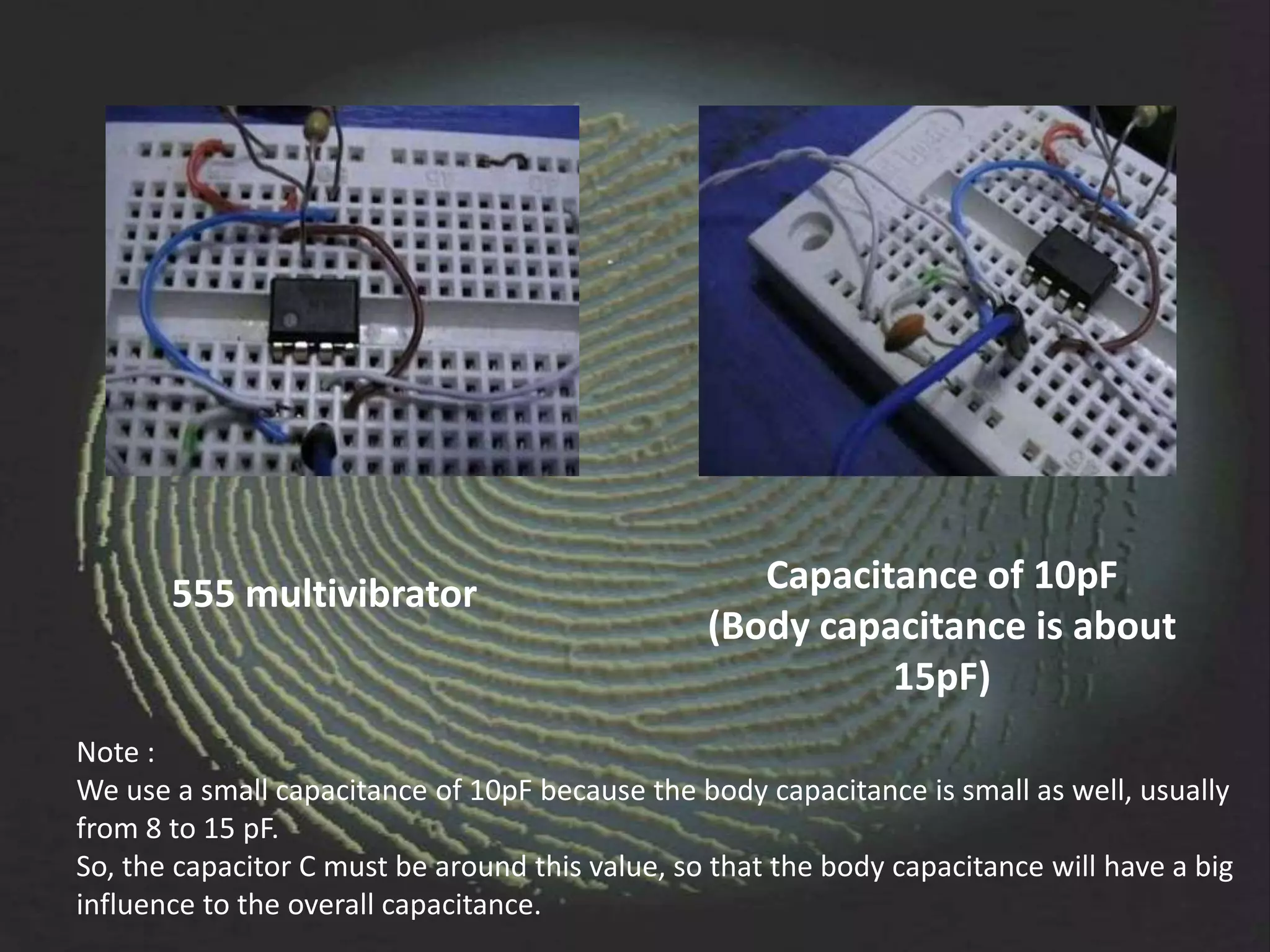
Downloaded 405 times
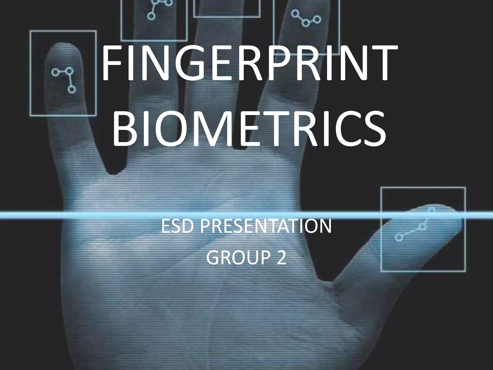
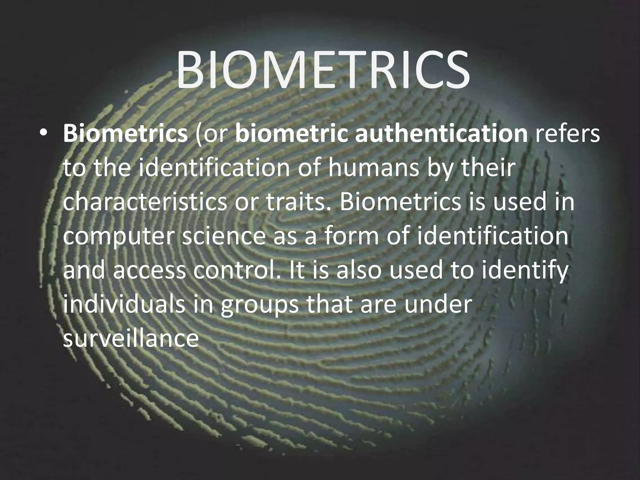
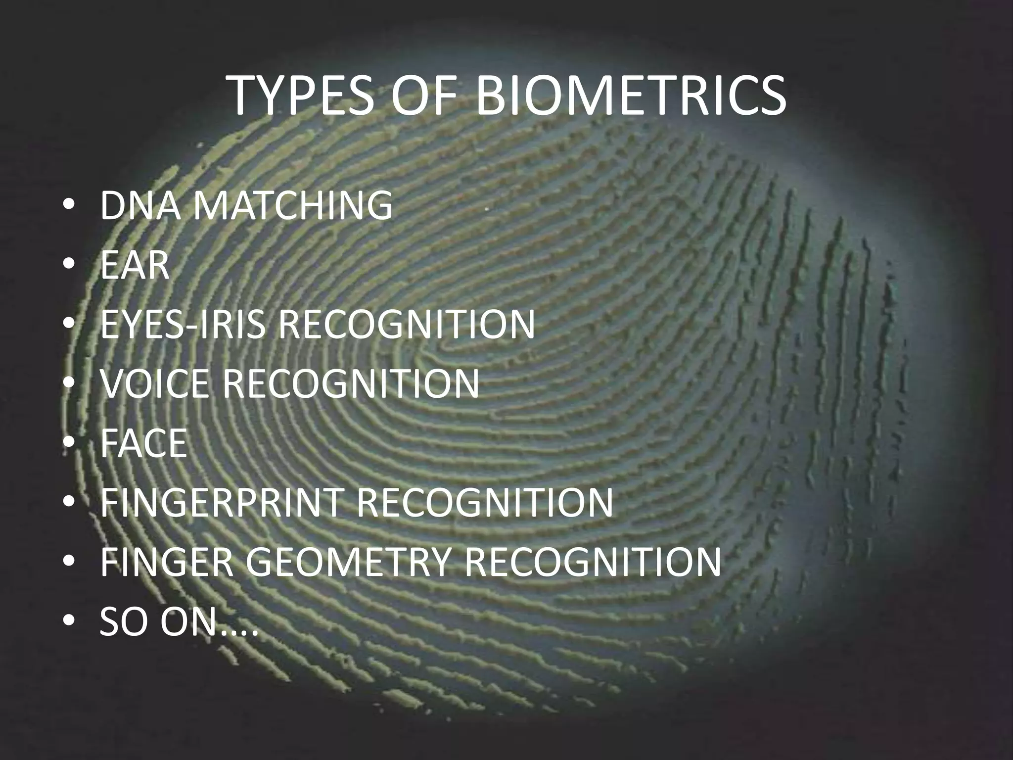
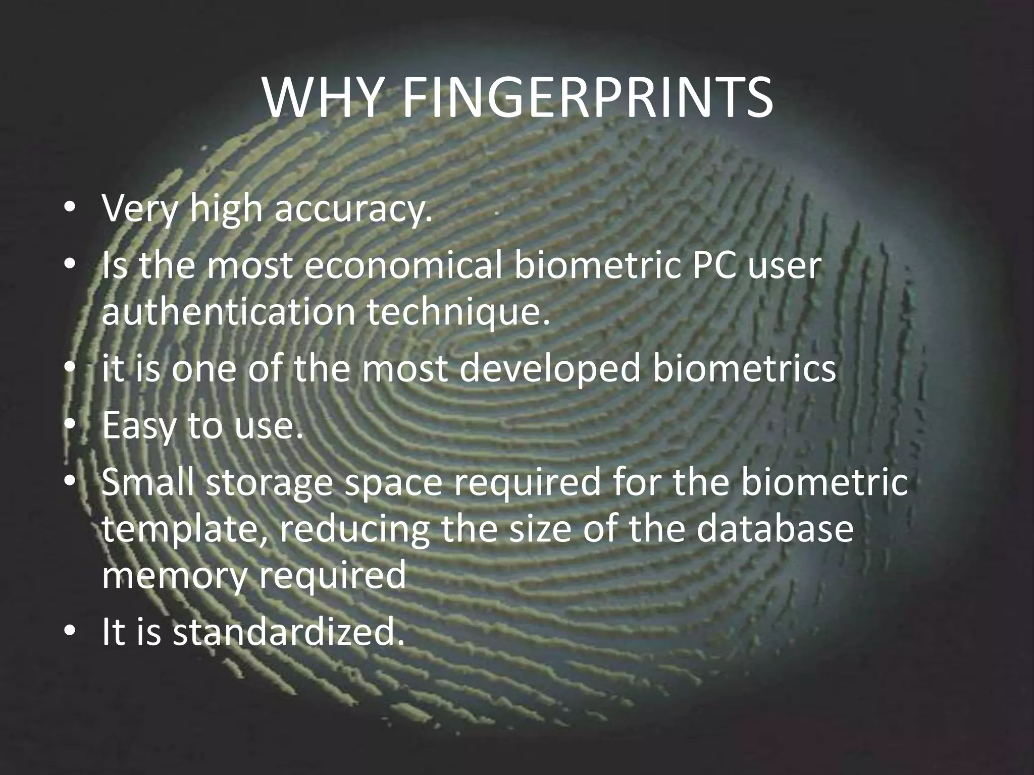

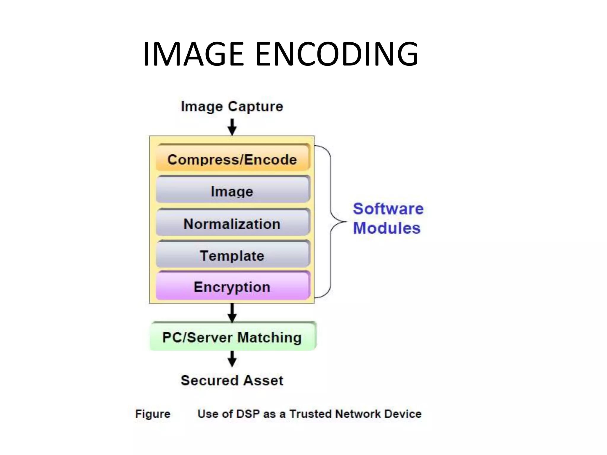
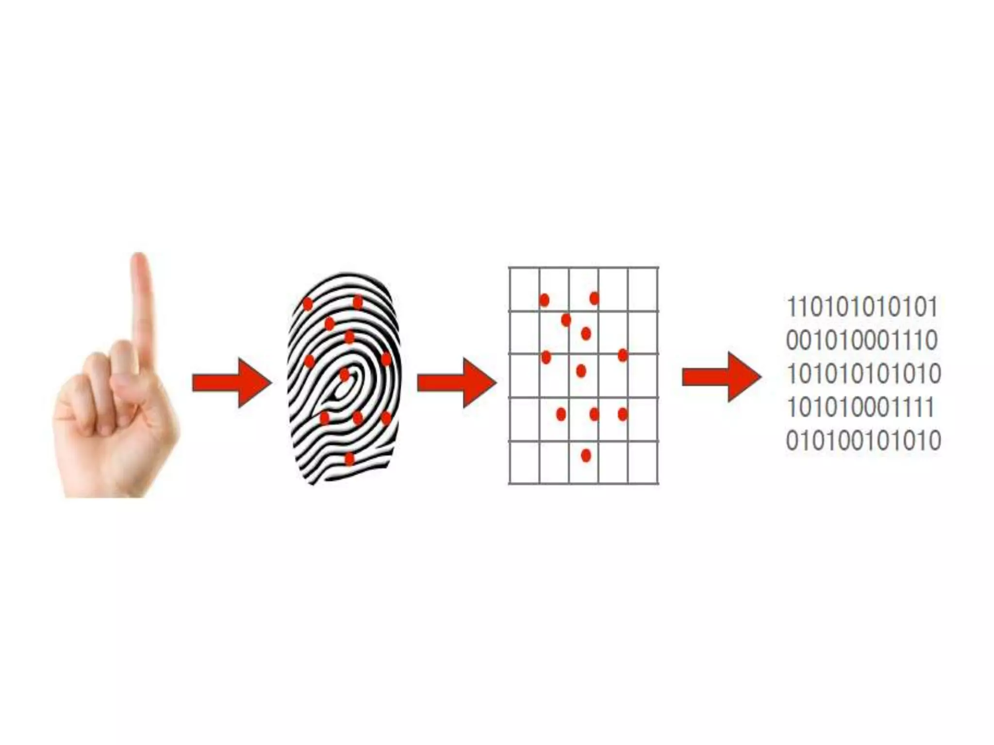


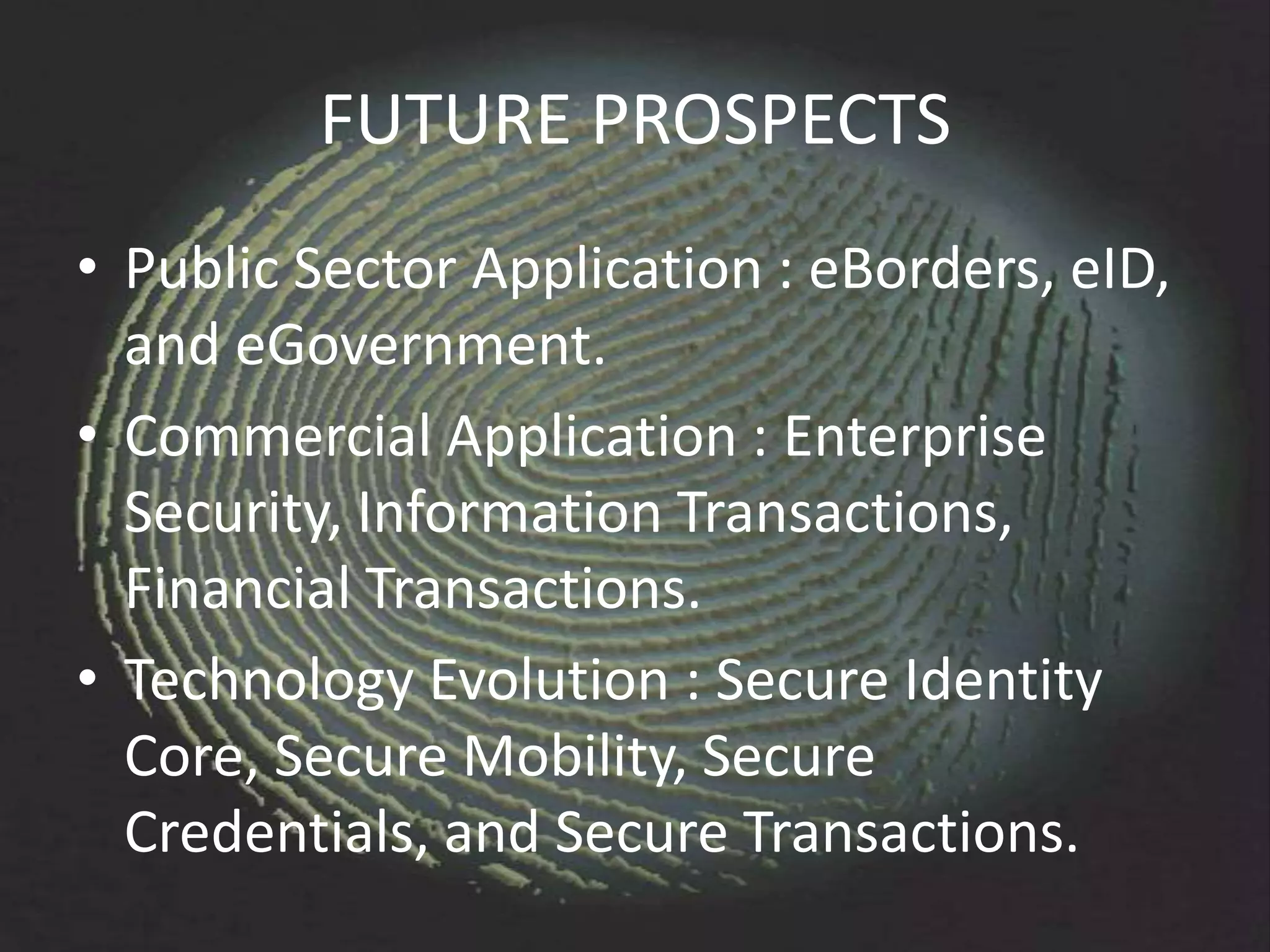
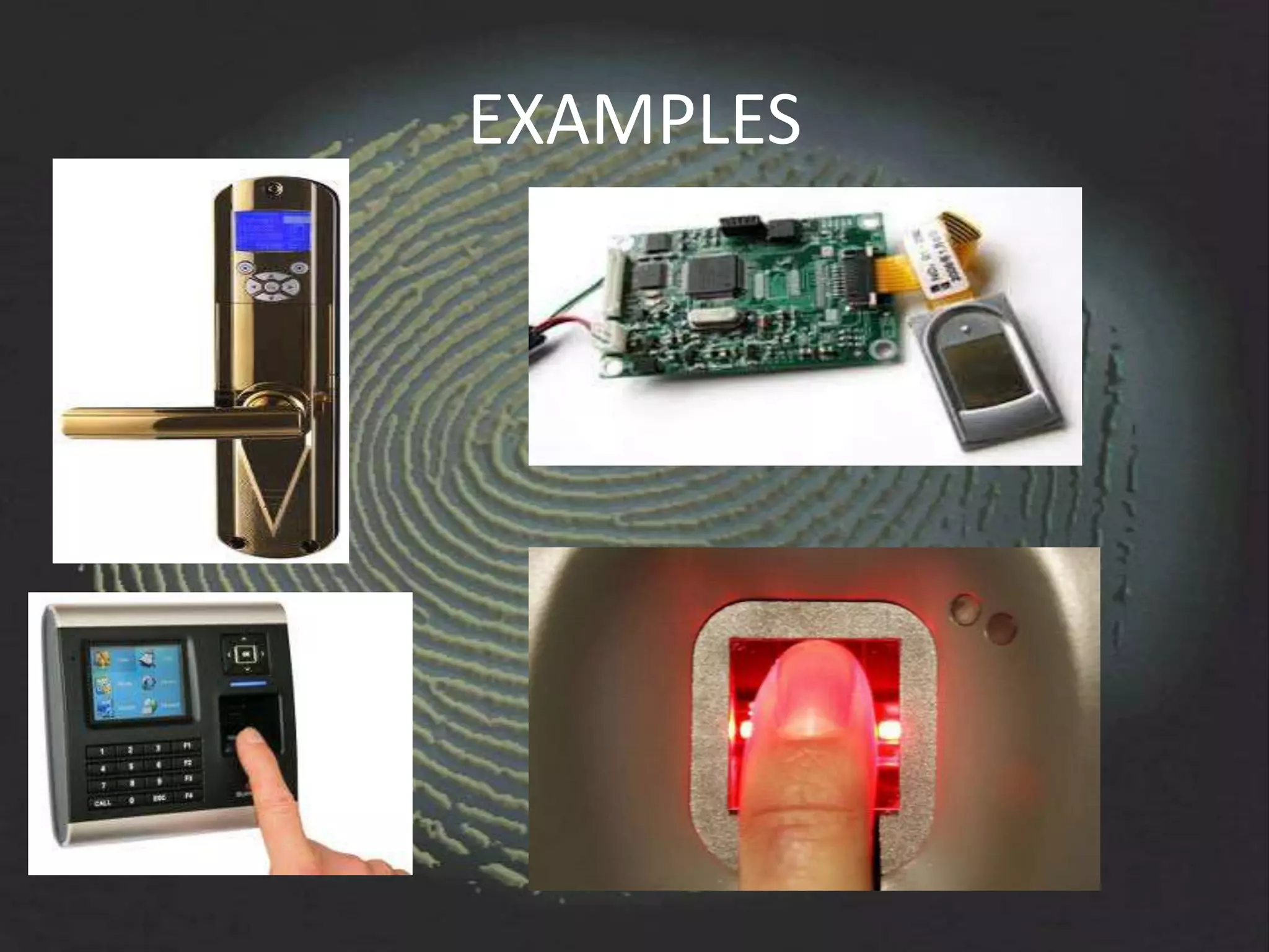

The document provides an overview of fingerprint biometrics, detailing its significance, methods of operation, and various technologies used in authentication systems. It discusses different sensor types, processing elements, and the advantages of digital signal processors for handling biometric data. Future prospects for biometrics include applications in public sectors and commercial uses, emphasizing the evolution of secure identity and transaction technologies.


