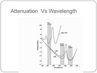
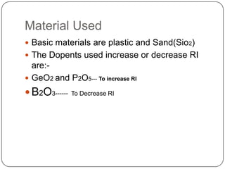
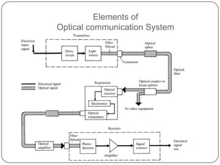
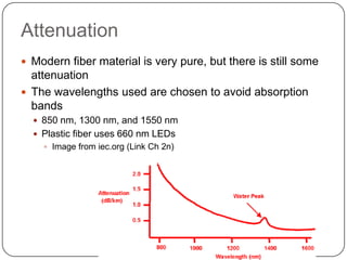
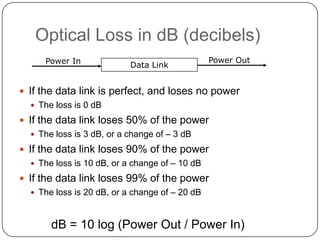
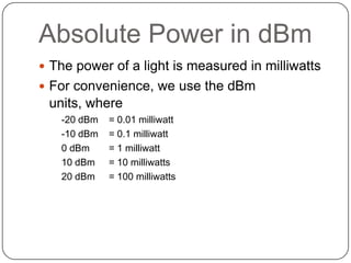
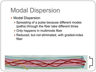
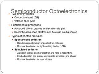
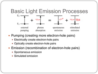
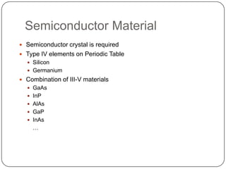
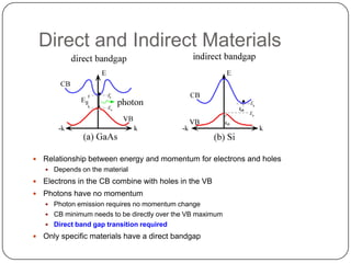
The document summarizes key aspects of optical fiber communication including:
1) It describes the advantages of optical fiber communication over copper wire communication such as smaller size, lower transmission loss, higher bandwidth, and immunity to electromagnetic interference.
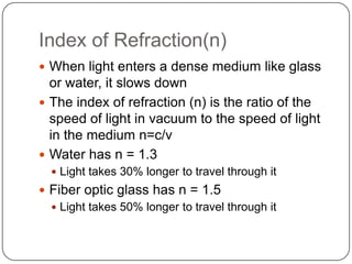
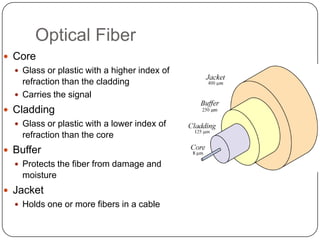
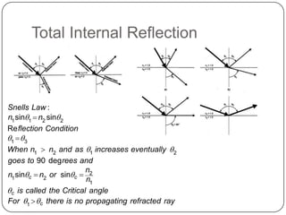
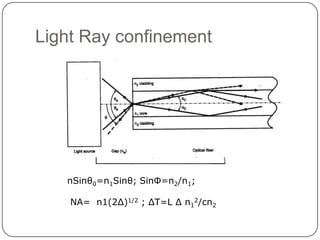
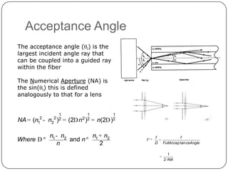
2) The basic components of an optical fiber are described including the core, cladding, buffer, and jacket. Total internal reflection is explained as the mechanism that guides light through the fiber.
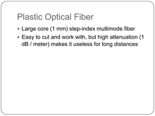
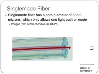
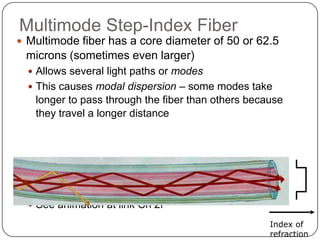
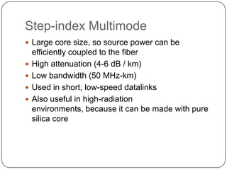
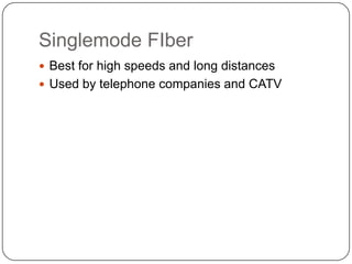
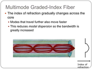
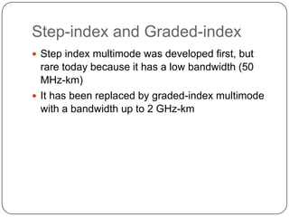
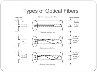
3) Different types of optical fibers are discussed including plastic optical fiber, single-mode fiber, multimode step-index fiber, and multimode graded-index fiber.


![PM [D02] de Broglie deriving the Equation](https://cdn.slidesharecdn.com/ss_thumbnails/pmd02debrogliederivingtheequation-151027082549-lva1-app6892-thumbnail.jpg?width=640&height=640&fit=bounds)


