Downloaded 398 times
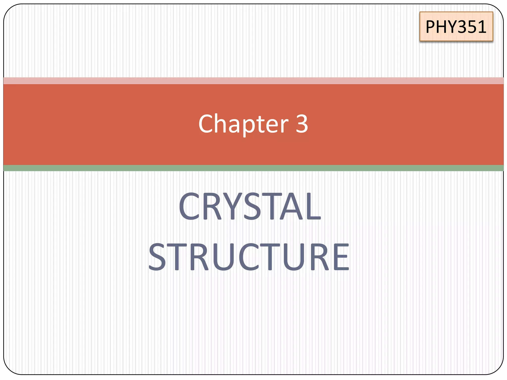
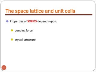
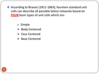
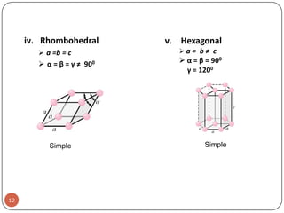
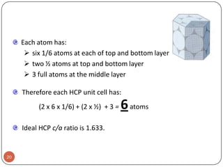
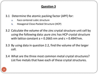
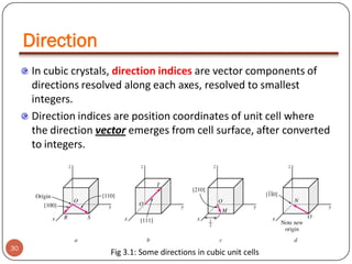
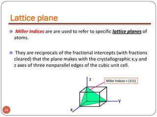
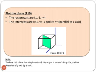
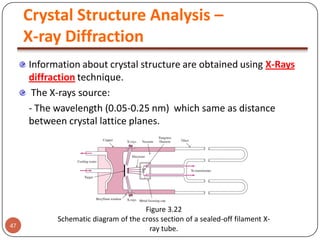
![PROCEDURE TO FIND DIRECTION INDICES
Produce the direction vector till it
emerges from surface of cubic cell
z
(1,1/2,1)
Determine the coordinates of point
of emergence and origin
(1,1/2,1) - (0,0,0)
= (1,1/2,1)
y
(0,0,0)
Subtract coordinates of point of
Emergence by that of origin
Are all are
integers?
YES
Are any of the direction
vectors negative?
YES
31
Represent the indices in a square
bracket without comas with a
over negative index (Eg: [121])
NO
x
2 x (1,1/2,1)
= (2,1,2)
The direction indices are [212]
Convert them to
smallest possible
integer by multiplying
by an integer.
NO
Represent the indices in a square
bracket without comas (Eg: [212] )](https://image.slidesharecdn.com/phy351ch3-131102034635-phpapp01/85/Phy351-ch-3-31-320.jpg)
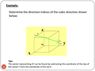
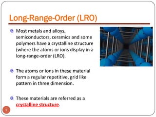
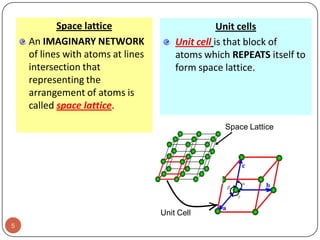
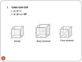
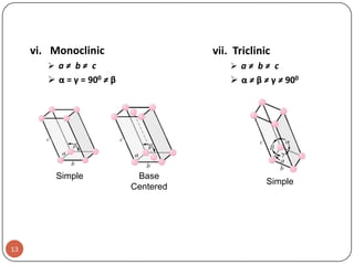
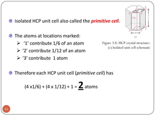
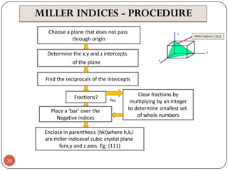
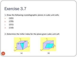
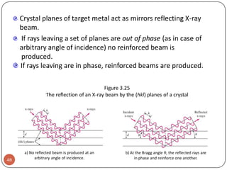
![Exercise 3.4
i.
ii.
33
Draw the following direction vectors in cubic unit cells:
a. [100] and [110]
b. [112]
c. [1 1 0]
d. [3 2 1]
Determine the direction indices of the cubic direction
between the position coordinates (3/4 , 0 , ¼) and (1/4 ,
½ , ½)](https://image.slidesharecdn.com/phy351ch3-131102034635-phpapp01/85/Phy351-ch-3-33-320.jpg)
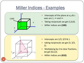
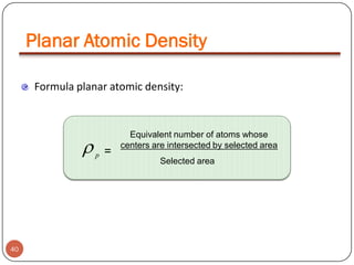
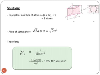
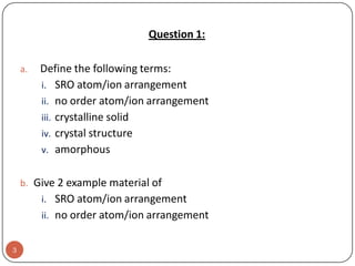
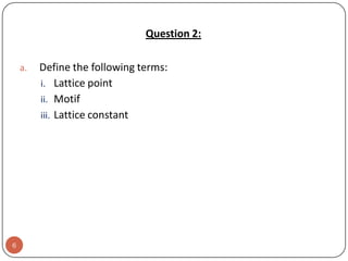
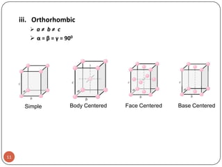
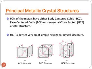
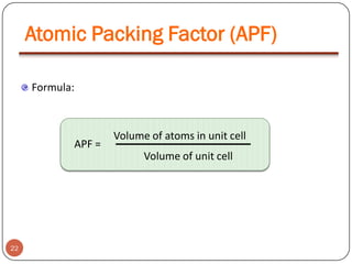
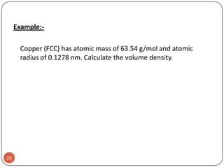
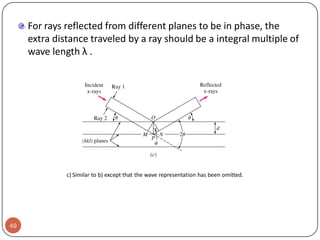
![Example:For a FCC copper crystal (a=0.361 nm), the [110] direction
intersects 2 half diameters and 1 full diameter.
44](https://image.slidesharecdn.com/phy351ch3-131102034635-phpapp01/85/Phy351-ch-3-44-320.jpg)

This document discusses crystal structure and properties of solids. It begins by defining long-range order and crystalline structure, noting that most metals, semiconductors, and some other materials have crystalline structure with atoms arranged in a repetitive grid pattern. It then discusses basic terms like unit cell and space lattice, and describes the seven crystal systems and 14 Bravais lattices. Common metallic crystal structures of body-centered cubic, face-centered cubic, and hexagonal close-packed are discussed. Finally, it touches on X-ray diffraction techniques used to analyze crystal structure.


