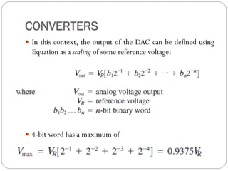
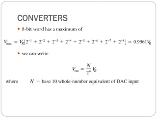
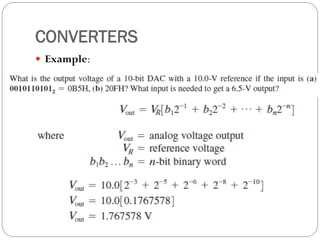
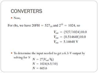
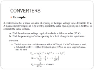
Compiled by: Prof. G B Rathod
EC Dept., BVM Engineering college.
Email: ghansyam.rathod@bvmengineering.ac.in
Digital signal conditioning
Outlines
 Review of Digital Fundamentals
 Converters
 DataAcquisition systems
 Characteristics of Digital Data
Review of Digital Fundamentals
 Digital Information
 The use of digital techniques in process control requires that
process variable measurements and control information be
encoded into a digital form.
 Digital signals themselves are simply two-state (binary)
levels.These levels may be represented in many ways.
 The individual digital levels are referred to as bits of the
word. Thus, for example, a 6-bit word consists of six
independent digital levels, such as 110110 which can be
thought of as a six-digit base 2 number.
Review of Digital Fundamentals
 Decimal Whole Numbers One of the most common schemes
for encoding analog data into a digital word is to use the straight
counting of decimal (or base 10) and binary number
representations.
 Octal and Hex Numbers It is cumbersome for humans to work
with digital words expressed as numbers in the binary
representation. For this reason, it has become common to use
either the octal (base 8) or hexadecimal (base 16, called hex)
representations.
 Fractional Binary Numbers: Although not as commonly used,
it is possible to define a fractional binary number in the same
manner as whole numbers, using only the 1 and 0 of this counting
system.
Review of Digital Fundamentals
 Such numbers, just as in the decimal framework, represent
divisions of the counting system to values less than unity.
 Boolean Algebra:
 Let us consider a simple example of how a Boolean equation
may result from a practical problem
 The alarm will be triggered when the Boolean variable D
goes to the logic true state.The alarm conditions are
 1. Low level with high pressure
 2. High level with high temperature
 3. High level with low temperature and high pressure
Review of Digital Fundamentals
 We now define a Boolean expression with AND operations
that will give a D=1 for each condition:
Review of Digital Fundamentals
 The final logic equation results from combining all three
conditions so that if any is true, the alarm will sound D=1 .
This is accomplished with the OR operation
 This equation would now form the starting point for a design
of electronic digital circuitry that would perform the
indicated operations.
Review of Digital Fundamentals
 Programmable Logic Controllers.
 The move toward digital logic techniques and computers in
industrial control paralleled the development of special
controllers called programmable logic controllers (PLCs), or
simply programmable controllers (PCs).
 These devices are particularly suited to the solution control
problems associated with Boolean equations and binary logic
problems in general. They are a computer-based outgrowth
of relay sequence controllers.
Review of Digital Fundamentals
 Computer Interface
 Figure shows a simple model of a computer system. The
processor is connected to external equipment via three
parallel sets of digital lines.
Fig: Generic Model of Computer
Bus system
Review of Digital Fundamentals
 The data lines carry data to and from the processor. The
address lines allow the computer to select external locations
for input and output. The control lines carry information to
and from the computer related to operations, such as
reading, writing, interrupts, and so on.
 This collection of lines is called the bus of the computer.
 The term interface refers to the hardware connections and
software operations necessary to input and output data using
connections to the bus
Review of Digital Fundamentals
 Tri-State Buffers Isolation of a bus line is accomplished by
making all connections via a special digital device called a tri-
state buffer.
 This device acts like a simple switch. When the switch is
closed, the logic level on its input is impressed upon the
output. When open, the output is placed in a high-impedance
state—that is, an open circuit.
Fig:Tri-state buffers allow multiple signals
to share a single digital line in the bus.
Review of Digital Fundamentals
 Last Figure shows how two digital signals can both be
connected to a single data line through tri-state buffers.
 Normally, both tri-states are disabled—that is, in the high
impedance state. When the computer needs to input signal A,
an enable signal, E1, is sent to tri-state 1 so that the state of A
is placed on the data line
 After the computer reads the line, tri-state 1 is disabled
again. Similarly, when the computer needs the state of signal
B, an enable, E2, is sent to tri-state 2 to place B on the line.
CONVERTERS
 The most important digital tool for the process-control
technologist is one that translates digital information to
analog and vice versa.
 Most measurements of process variables are performed by
devices that translate information about the variable to an
analog electrical signal.
 Comparators:
 The most elementary form of communication between the
analog and digital is a device (usually an IC) called a
comparator.
CONVERTERS
 This device, which is shown schematically in Figure , simply
compares two analog voltages on its input terminals.
 Depending on which voltage is larger, the output will be a 1
(high) or a 0 (low) digital signal. The comparator is
extensively used for alarm signals to computers or digital
processing systems.
CONVERTERS
 The comparator is extensively used for alarm signals to
computers or digital processing systems.
 EXAMPLE
 Solution:
CONVERTERS
CONVERTERS
 Open-Collector Comparators Some comparator models
have a special method of providing the digital output signal.
 Figure shows that the output terminal of the comparator is
connected internally to the collector of a transistor in the
comparator and nowhere else! This is called an open-collector
output because it is just that.
CONVERTERS
 Hysteresis Comparator When using comparators, there is
often a problem if the signal voltage has noise or approaches
the reference value too slowly.
 The comparator output may “jiggle” back and forth between
high and low as the reference level is reached. This effect is
shown in Figure.
CONVERTERS
 Such fluctuation of output shows in last figure may cause problems
with the equipment designed to interpret the comparator output
signal.
 This problem can often be solved by providing a deadband or
hysteresis window to the reference level around which output
changes occur.
 Once the comparator has been triggered high, the reference level
is automatically reduced so that the signal must fall to some value
below the old reference before the comparator goes to the low
state.
 There are many ways this hysteresis can be provided, but
upcoming Figure shows one common technique.
CONVERTERS
 Feedback resistor Rf is provided between the output and one
of the inputs of the comparator, and that input is separated
from the signal by another resistor, R. Under the condition
that Rf >>R , the response of the comparator is shown in
Figure a and b.
CONVERTERS
 Digital-to-Analog Converters (DACs)
 ADAC accepts digital information and transforms it into an
analog voltage. The digital information is in the form of a
binary number with some fixed number of digits.
 A unipolar DAC converts a digital word into an analog
voltage by scaling the analog output to be zero when all bits
are zero and some maximum value when all bits are one.
 This can be mathematically represented by treating the
binary number that the word represents as a fractional
number.
CONVERTERS
 In this context, the output of the DAC can be defined using
Equation as a scaling of some reference voltage:
 4-bit word has a maximum of
CONVERTERS
 8-bit word has a maximum of
 we can write
CONVERTERS
 Example:
CONVERTERS
 Now,
 To determine the input needed to get a 6.5-V output by
solving for N,
CONVERTERS
 The fact that there is a fractional remainder tells us that we
cannot get exactly 6.5 V from the converter. The best we can
do is get an output for N= 665 = 229H or 666 =29A H.
 The outputs for these two inputs are 6.494 V and 6.504 V,
respectively. The only way to get exactly 6.5 V of output
would be to change the value of the reference slightly.
 Bipolar DAC Some DACs are designed to output a voltage
that ranges from plus to minus some maximum when the
input binary ranges over the counting states.
CONVERTERS
 Although computers frequently use 2s complement to
represent negative numbers, this is not common with DACs.
 Instead, a simple offset-binary is frequently used, wherein the
output is simply biased by half the reference voltage of
Equation.The bipolar DAC relationship is then given by
 Notice that if N=0 , the output voltage will be given by the
minimum value,Vout= -VR/2 and Maximum value ofVout is
CONVERTERS
 Example:
CONVERTERS
 When zero occurs,Vout=0, so solving N gives
 Conversion Resolution The conversion resolution is a
function of the reference voltage and the number of bits in
the word.
 The more bits, the smaller the change in analog output for a
1-bit change in binary word, and hence the better the
resolution.The smallest possible change is simply given by
CONVERTERS
 Here,
 Example:
CONVERTERS
 We can use the equation,
 Here,
 To get the y, take a log both the side
CONVERTERS
 If we take n=8, we get the output as per below
 Which is in the range of 0.04 and that is accepted.
 DAC Characteristics :
 For modern applications, most DACs are integrated circuit
(IC) assemblies, viewed as a black box having certain input
and output characteristics.
CONVERTERS
Fig:A generic DAC diagram,
showing typical input
and output signals
CONVERTERS
 Offset Because the DAC is usually implemented with op amps,
there may be the typical output offset voltage with a zero input.
Typically, connections will be provided to facilitate a zeroing of the
DAC output with a zero word input.
 Data latch Many DACs have a data latch built into their inputs.
When a logic command is given to latch data, whatever data are
on the input bus will be latched into the DAC, and the analog
output will be updated for that input data.
 The output will stay at that value until new digital data are latched
into the input.
 In this way, the input of the DAC can be connected directly onto
the data bus of a computer, but it will be updated only when a
latch command is given by the computer.
CONVERTERS
 Example:
CONVERTERS
 The figure: typical
DAC is often
implemented
using a ladder
network of
resistors
CONVERTERS
 Solution for b:
CONVERTERS
 Analog-to-Digital Converters (ADCs)
 Although there are sensors that provide a direct digital signal output and more
are being developed, most still convert the measured variable into an analog
electrical signal.
 With the growing use of digital logic and computers in process control, it is
necessary to employ an ADC to provide a digitally encoded signal for the
computer.
 The transfer function of the ADC can be expressed in a similar way to that of
the DAC as given in Equation
CONVERTERS
 Inherent uncertainty in the input voltage producing a given
ADC output, and that uncertainty is given by
 Example:
CONVERTERS
 Here,
CONVERTERS
 Here,
 Example:
CONVERTERS
 Using the method of successive multiplication, we get
CONVERTERS
 Equation can be written in a simpler fashion by expressing
the fractional binary number as the fraction of counting
states, as was done for the DAC. In this case, the base 10
value of the digital output can be expressed as
 Example:
CONVERTERS
 We can use the last equation, where
 Now, for
CONVERTERS
 However, it is important to realize that any voltage from this
to 1.06445 + 2.5/1024 = 1.06689 will give the same
output, 1B4H. So the correct answer to the question is that
the input voltage lies in the range 1.06445 to 1.06689V.
 Bipolar Operation A bipolar ADC is one that accepts
bipolar input voltage for conversion into an appropriate
digital output.
 The most common bipolar ADCs provide an output called
offset-binary. This simply means that the normal output is
shifted by half the scale so that all-zeros corresponds to the
negative maximum input voltage instead of zero. In equation
form, the relation would be written as
CONVERTERS
 Continue…
CONVERTERS
 ADC Diagram:
 SC
 (Start-convert)
 EOC
 (End-of-convert)
 RD (Read)
CONVERTERS
 The limitations on frequency severely limit the application of
ADCs and computer data-acquisition systems.
 There is a solution, however. What is needed is simply that
the signal not change during the conversion process.
 Therefore, the answer is to hold the value constant during
that process. This is accomplished with a sample-and-hold
(S/H) circuit.
 Sample-and-Hold The basic concept of the sample-and-
hold circuit is shown in upcoming Figure , where the S/H is
connected to the input of an ADC
CONVERTERS
 When the electronic switch is closed, the capacitor voltage
will “track” the input voltage,Vc(t)=Vin(t).
 At some time ts, when a conversion of the input voltage is
desired, the electronic switch is opened isolating the
capacitor from the input. Thus, the capacitor will hold (stay
charged) to the voltage when the switch opened,Vc =Vin(ts)
CONVERTERS
 Figure:The sampled signal is literally “held” during the ADC
conversion process.
DATA-ACQUISITION SYSTEMS
 Microprocessor-based personal computers (PCs) are used
extensively to implement direct digital control in the process
industries.
 These familiar desktop computers are designed much like the
system shown in upcoming Figure 24, using a bus that consists of
the data lines, address lines, and control lines.
 All communication with the processor is via these bus lines. This
includes essential equipment such as RAM, ROM, disk, and CD-
ROM.
 Special PCBs called data-acquisition systems (DASs) have been
developed for the purpose of providing for input and output of
analog data.
DATA-ACQUISITION SYSTEMS
 Fig:An ADC can be
interfaced directly to
the computer bus if
it has tri-state outputs.
Address decoding is
required so the
ADC can be operated
by computer software.
DATA-ACQUISITION SYSTEMS
 The PC also connects the bus lines to a number of printed
circuit board (PCB) sockets, using an industry standard
configuration of how the bus lines are connected to the
socket.These sockets are referred to as expansion slots.
 DAS Hardware
 The hardware features of a general data-acquisition system
are shown in upcoming Figure . Although there is variation
from manufacturer to manufacturer, the system shown in this
figure and described herein demonstrates the essential
features of DASs.
DATA-ACQUISITION SYSTEMS
 Fig:Typical layout of a data-acquisition board for use in a
personal computer expansion slot.
DATA-ACQUISITION SYSTEMS
 ADC and S/H The DAS typically has a high-speed, successive
approximation type ADC and a fast S/H circuit.
 Whenever the DAS is requested to obtain a data sample, the S/H is
automatically incorporated into the process.
 Analog Multiplexer The analog multiplexer (MUX) allows the DAS
to select data from a number of different sources. The MUX has a
number of input channels, each of which is connected to a different
analog input voltage source.
 Address Decoder/Command Processor The computer can select
to input a sample from a given channel by sending an appropriate
selection on the address lines and control lines of the computer bus.
 DAC and Latch For output purposes, the DAS often includes a latch
and DAC. The address decoder/command processor is used to latch data
written to the DAS, which is then converted to an appropriate analog
signal by the DAC.
DATA-ACQUISITION SYSTEMS
 DAS Software
 The process of selecting a channel and initiating a data input
from that channel involves some interface between the
computer and the DAS.
 This interface is facilitated by software that the computer
executes. The software can be written by the user, but is
often also provided by the DAS manufacturer in the form of
programs on disk.
 Figure is a flowchart of the basic sequence of operations that
must occur when a sample is required from the DAS.
DATA-ACQUISITION SYSTEMS
 Fig: Software for data acquisition involves operations to start
theADC, test the EOC, and input the data.
CHARACTERISTICS OF DIGITAL DATA
 DigitizedValue
 Consider first analog-to-digital conversion (ADC) of analog data
into a digital format. The format of the ADC output is an n-bit
binary representation of the data.
 With n-bits it is possible to represent 2^n values, including zero.
There is a finite resolution of the physical data being represented of
one part in 2^n, and that means we now are ignorant about the
value of the variable after it has been converted into the binary
representation.
 Sampled Data Systems: For the control system to function
correctly, certain conditions must be assumed about variations
between samples.That is what sampled data systems are all about.
CHARACTERISTICS OF DIGITAL DATA
 Sampling Rate The key issue with respect to sampling in a
computer-based controller is the rate at which samples must
be taken.
 There is a maximum sampling rate in any system—that is,
the time required to take a sample (ADC conversion time)
plus the time required to solve the controller equations to
determine the appropriate output (program execution time).
 There is a minimum sampling rate in any system that depends
on the nature of the time variation of the sampled variable.
CHARACTERISTICS OF DIGITAL DATA
 Linearization:
 In many cases, the input binary number and the controlled
variable are not linearly related. In such cases, it is necessary
to execute a program that will linearize the binary number so
that it is proportional to the controlled variable value.
Reference
 Curtis D. Johnson.“Process Control Instrumentation
Technology”, Prentice Hall, 8/E, 2005 ISBN-10:
0131194577 • ISBN-13: 9780131194571
Thank You

Digital Signal Conditioning

  • 1.
    Compiled by: Prof.G B Rathod EC Dept., BVM Engineering college. Email: ghansyam.rathod@bvmengineering.ac.in Digital signal conditioning
  • 2.
    Outlines  Review ofDigital Fundamentals  Converters  DataAcquisition systems  Characteristics of Digital Data
  • 3.
    Review of DigitalFundamentals  Digital Information  The use of digital techniques in process control requires that process variable measurements and control information be encoded into a digital form.  Digital signals themselves are simply two-state (binary) levels.These levels may be represented in many ways.  The individual digital levels are referred to as bits of the word. Thus, for example, a 6-bit word consists of six independent digital levels, such as 110110 which can be thought of as a six-digit base 2 number.
  • 4.
    Review of DigitalFundamentals  Decimal Whole Numbers One of the most common schemes for encoding analog data into a digital word is to use the straight counting of decimal (or base 10) and binary number representations.  Octal and Hex Numbers It is cumbersome for humans to work with digital words expressed as numbers in the binary representation. For this reason, it has become common to use either the octal (base 8) or hexadecimal (base 16, called hex) representations.  Fractional Binary Numbers: Although not as commonly used, it is possible to define a fractional binary number in the same manner as whole numbers, using only the 1 and 0 of this counting system.
  • 5.
    Review of DigitalFundamentals  Such numbers, just as in the decimal framework, represent divisions of the counting system to values less than unity.  Boolean Algebra:  Let us consider a simple example of how a Boolean equation may result from a practical problem  The alarm will be triggered when the Boolean variable D goes to the logic true state.The alarm conditions are  1. Low level with high pressure  2. High level with high temperature  3. High level with low temperature and high pressure
  • 6.
    Review of DigitalFundamentals  We now define a Boolean expression with AND operations that will give a D=1 for each condition:
  • 7.
    Review of DigitalFundamentals  The final logic equation results from combining all three conditions so that if any is true, the alarm will sound D=1 . This is accomplished with the OR operation  This equation would now form the starting point for a design of electronic digital circuitry that would perform the indicated operations.
  • 8.
    Review of DigitalFundamentals  Programmable Logic Controllers.  The move toward digital logic techniques and computers in industrial control paralleled the development of special controllers called programmable logic controllers (PLCs), or simply programmable controllers (PCs).  These devices are particularly suited to the solution control problems associated with Boolean equations and binary logic problems in general. They are a computer-based outgrowth of relay sequence controllers.
  • 9.
    Review of DigitalFundamentals  Computer Interface  Figure shows a simple model of a computer system. The processor is connected to external equipment via three parallel sets of digital lines. Fig: Generic Model of Computer Bus system
  • 10.
    Review of DigitalFundamentals  The data lines carry data to and from the processor. The address lines allow the computer to select external locations for input and output. The control lines carry information to and from the computer related to operations, such as reading, writing, interrupts, and so on.  This collection of lines is called the bus of the computer.  The term interface refers to the hardware connections and software operations necessary to input and output data using connections to the bus
  • 11.
    Review of DigitalFundamentals  Tri-State Buffers Isolation of a bus line is accomplished by making all connections via a special digital device called a tri- state buffer.  This device acts like a simple switch. When the switch is closed, the logic level on its input is impressed upon the output. When open, the output is placed in a high-impedance state—that is, an open circuit. Fig:Tri-state buffers allow multiple signals to share a single digital line in the bus.
  • 12.
    Review of DigitalFundamentals  Last Figure shows how two digital signals can both be connected to a single data line through tri-state buffers.  Normally, both tri-states are disabled—that is, in the high impedance state. When the computer needs to input signal A, an enable signal, E1, is sent to tri-state 1 so that the state of A is placed on the data line  After the computer reads the line, tri-state 1 is disabled again. Similarly, when the computer needs the state of signal B, an enable, E2, is sent to tri-state 2 to place B on the line.
  • 13.
    CONVERTERS  The mostimportant digital tool for the process-control technologist is one that translates digital information to analog and vice versa.  Most measurements of process variables are performed by devices that translate information about the variable to an analog electrical signal.  Comparators:  The most elementary form of communication between the analog and digital is a device (usually an IC) called a comparator.
  • 14.
    CONVERTERS  This device,which is shown schematically in Figure , simply compares two analog voltages on its input terminals.  Depending on which voltage is larger, the output will be a 1 (high) or a 0 (low) digital signal. The comparator is extensively used for alarm signals to computers or digital processing systems.
  • 15.
    CONVERTERS  The comparatoris extensively used for alarm signals to computers or digital processing systems.  EXAMPLE  Solution:
  • 16.
  • 17.
    CONVERTERS  Open-Collector ComparatorsSome comparator models have a special method of providing the digital output signal.  Figure shows that the output terminal of the comparator is connected internally to the collector of a transistor in the comparator and nowhere else! This is called an open-collector output because it is just that.
  • 18.
    CONVERTERS  Hysteresis ComparatorWhen using comparators, there is often a problem if the signal voltage has noise or approaches the reference value too slowly.  The comparator output may “jiggle” back and forth between high and low as the reference level is reached. This effect is shown in Figure.
  • 19.
    CONVERTERS  Such fluctuationof output shows in last figure may cause problems with the equipment designed to interpret the comparator output signal.  This problem can often be solved by providing a deadband or hysteresis window to the reference level around which output changes occur.  Once the comparator has been triggered high, the reference level is automatically reduced so that the signal must fall to some value below the old reference before the comparator goes to the low state.  There are many ways this hysteresis can be provided, but upcoming Figure shows one common technique.
  • 20.
    CONVERTERS  Feedback resistorRf is provided between the output and one of the inputs of the comparator, and that input is separated from the signal by another resistor, R. Under the condition that Rf >>R , the response of the comparator is shown in Figure a and b.
  • 21.
    CONVERTERS  Digital-to-Analog Converters(DACs)  ADAC accepts digital information and transforms it into an analog voltage. The digital information is in the form of a binary number with some fixed number of digits.  A unipolar DAC converts a digital word into an analog voltage by scaling the analog output to be zero when all bits are zero and some maximum value when all bits are one.  This can be mathematically represented by treating the binary number that the word represents as a fractional number.
  • 22.
    CONVERTERS  In thiscontext, the output of the DAC can be defined using Equation as a scaling of some reference voltage:  4-bit word has a maximum of
  • 23.
    CONVERTERS  8-bit wordhas a maximum of  we can write
  • 24.
  • 25.
    CONVERTERS  Now,  Todetermine the input needed to get a 6.5-V output by solving for N,
  • 26.
    CONVERTERS  The factthat there is a fractional remainder tells us that we cannot get exactly 6.5 V from the converter. The best we can do is get an output for N= 665 = 229H or 666 =29A H.  The outputs for these two inputs are 6.494 V and 6.504 V, respectively. The only way to get exactly 6.5 V of output would be to change the value of the reference slightly.  Bipolar DAC Some DACs are designed to output a voltage that ranges from plus to minus some maximum when the input binary ranges over the counting states.
  • 27.
    CONVERTERS  Although computersfrequently use 2s complement to represent negative numbers, this is not common with DACs.  Instead, a simple offset-binary is frequently used, wherein the output is simply biased by half the reference voltage of Equation.The bipolar DAC relationship is then given by  Notice that if N=0 , the output voltage will be given by the minimum value,Vout= -VR/2 and Maximum value ofVout is
  • 28.
  • 29.
    CONVERTERS  When zerooccurs,Vout=0, so solving N gives  Conversion Resolution The conversion resolution is a function of the reference voltage and the number of bits in the word.  The more bits, the smaller the change in analog output for a 1-bit change in binary word, and hence the better the resolution.The smallest possible change is simply given by
  • 30.
  • 31.
    CONVERTERS  We canuse the equation,  Here,  To get the y, take a log both the side
  • 32.
    CONVERTERS  If wetake n=8, we get the output as per below  Which is in the range of 0.04 and that is accepted.  DAC Characteristics :  For modern applications, most DACs are integrated circuit (IC) assemblies, viewed as a black box having certain input and output characteristics.
  • 33.
    CONVERTERS Fig:A generic DACdiagram, showing typical input and output signals
  • 34.
    CONVERTERS  Offset Becausethe DAC is usually implemented with op amps, there may be the typical output offset voltage with a zero input. Typically, connections will be provided to facilitate a zeroing of the DAC output with a zero word input.  Data latch Many DACs have a data latch built into their inputs. When a logic command is given to latch data, whatever data are on the input bus will be latched into the DAC, and the analog output will be updated for that input data.  The output will stay at that value until new digital data are latched into the input.  In this way, the input of the DAC can be connected directly onto the data bus of a computer, but it will be updated only when a latch command is given by the computer.
  • 35.
  • 36.
    CONVERTERS  The figure:typical DAC is often implemented using a ladder network of resistors
  • 37.
  • 38.
    CONVERTERS  Analog-to-Digital Converters(ADCs)  Although there are sensors that provide a direct digital signal output and more are being developed, most still convert the measured variable into an analog electrical signal.  With the growing use of digital logic and computers in process control, it is necessary to employ an ADC to provide a digitally encoded signal for the computer.  The transfer function of the ADC can be expressed in a similar way to that of the DAC as given in Equation
  • 39.
    CONVERTERS  Inherent uncertaintyin the input voltage producing a given ADC output, and that uncertainty is given by  Example:
  • 40.
  • 41.
  • 42.
    CONVERTERS  Using themethod of successive multiplication, we get
  • 43.
    CONVERTERS  Equation canbe written in a simpler fashion by expressing the fractional binary number as the fraction of counting states, as was done for the DAC. In this case, the base 10 value of the digital output can be expressed as  Example:
  • 44.
    CONVERTERS  We canuse the last equation, where  Now, for
  • 45.
    CONVERTERS  However, itis important to realize that any voltage from this to 1.06445 + 2.5/1024 = 1.06689 will give the same output, 1B4H. So the correct answer to the question is that the input voltage lies in the range 1.06445 to 1.06689V.  Bipolar Operation A bipolar ADC is one that accepts bipolar input voltage for conversion into an appropriate digital output.  The most common bipolar ADCs provide an output called offset-binary. This simply means that the normal output is shifted by half the scale so that all-zeros corresponds to the negative maximum input voltage instead of zero. In equation form, the relation would be written as
  • 46.
  • 47.
    CONVERTERS  ADC Diagram: SC  (Start-convert)  EOC  (End-of-convert)  RD (Read)
  • 48.
    CONVERTERS  The limitationson frequency severely limit the application of ADCs and computer data-acquisition systems.  There is a solution, however. What is needed is simply that the signal not change during the conversion process.  Therefore, the answer is to hold the value constant during that process. This is accomplished with a sample-and-hold (S/H) circuit.  Sample-and-Hold The basic concept of the sample-and- hold circuit is shown in upcoming Figure , where the S/H is connected to the input of an ADC
  • 49.
    CONVERTERS  When theelectronic switch is closed, the capacitor voltage will “track” the input voltage,Vc(t)=Vin(t).  At some time ts, when a conversion of the input voltage is desired, the electronic switch is opened isolating the capacitor from the input. Thus, the capacitor will hold (stay charged) to the voltage when the switch opened,Vc =Vin(ts)
  • 50.
    CONVERTERS  Figure:The sampledsignal is literally “held” during the ADC conversion process.
  • 51.
    DATA-ACQUISITION SYSTEMS  Microprocessor-basedpersonal computers (PCs) are used extensively to implement direct digital control in the process industries.  These familiar desktop computers are designed much like the system shown in upcoming Figure 24, using a bus that consists of the data lines, address lines, and control lines.  All communication with the processor is via these bus lines. This includes essential equipment such as RAM, ROM, disk, and CD- ROM.  Special PCBs called data-acquisition systems (DASs) have been developed for the purpose of providing for input and output of analog data.
  • 52.
    DATA-ACQUISITION SYSTEMS  Fig:AnADC can be interfaced directly to the computer bus if it has tri-state outputs. Address decoding is required so the ADC can be operated by computer software.
  • 53.
    DATA-ACQUISITION SYSTEMS  ThePC also connects the bus lines to a number of printed circuit board (PCB) sockets, using an industry standard configuration of how the bus lines are connected to the socket.These sockets are referred to as expansion slots.  DAS Hardware  The hardware features of a general data-acquisition system are shown in upcoming Figure . Although there is variation from manufacturer to manufacturer, the system shown in this figure and described herein demonstrates the essential features of DASs.
  • 54.
    DATA-ACQUISITION SYSTEMS  Fig:Typicallayout of a data-acquisition board for use in a personal computer expansion slot.
  • 55.
    DATA-ACQUISITION SYSTEMS  ADCand S/H The DAS typically has a high-speed, successive approximation type ADC and a fast S/H circuit.  Whenever the DAS is requested to obtain a data sample, the S/H is automatically incorporated into the process.  Analog Multiplexer The analog multiplexer (MUX) allows the DAS to select data from a number of different sources. The MUX has a number of input channels, each of which is connected to a different analog input voltage source.  Address Decoder/Command Processor The computer can select to input a sample from a given channel by sending an appropriate selection on the address lines and control lines of the computer bus.  DAC and Latch For output purposes, the DAS often includes a latch and DAC. The address decoder/command processor is used to latch data written to the DAS, which is then converted to an appropriate analog signal by the DAC.
  • 56.
    DATA-ACQUISITION SYSTEMS  DASSoftware  The process of selecting a channel and initiating a data input from that channel involves some interface between the computer and the DAS.  This interface is facilitated by software that the computer executes. The software can be written by the user, but is often also provided by the DAS manufacturer in the form of programs on disk.  Figure is a flowchart of the basic sequence of operations that must occur when a sample is required from the DAS.
  • 57.
    DATA-ACQUISITION SYSTEMS  Fig:Software for data acquisition involves operations to start theADC, test the EOC, and input the data.
  • 58.
    CHARACTERISTICS OF DIGITALDATA  DigitizedValue  Consider first analog-to-digital conversion (ADC) of analog data into a digital format. The format of the ADC output is an n-bit binary representation of the data.  With n-bits it is possible to represent 2^n values, including zero. There is a finite resolution of the physical data being represented of one part in 2^n, and that means we now are ignorant about the value of the variable after it has been converted into the binary representation.  Sampled Data Systems: For the control system to function correctly, certain conditions must be assumed about variations between samples.That is what sampled data systems are all about.
  • 59.
    CHARACTERISTICS OF DIGITALDATA  Sampling Rate The key issue with respect to sampling in a computer-based controller is the rate at which samples must be taken.  There is a maximum sampling rate in any system—that is, the time required to take a sample (ADC conversion time) plus the time required to solve the controller equations to determine the appropriate output (program execution time).  There is a minimum sampling rate in any system that depends on the nature of the time variation of the sampled variable.
  • 60.
    CHARACTERISTICS OF DIGITALDATA  Linearization:  In many cases, the input binary number and the controlled variable are not linearly related. In such cases, it is necessary to execute a program that will linearize the binary number so that it is proportional to the controlled variable value.
  • 61.
    Reference  Curtis D.Johnson.“Process Control Instrumentation Technology”, Prentice Hall, 8/E, 2005 ISBN-10: 0131194577 • ISBN-13: 9780131194571
  • 62.