Download to read offline
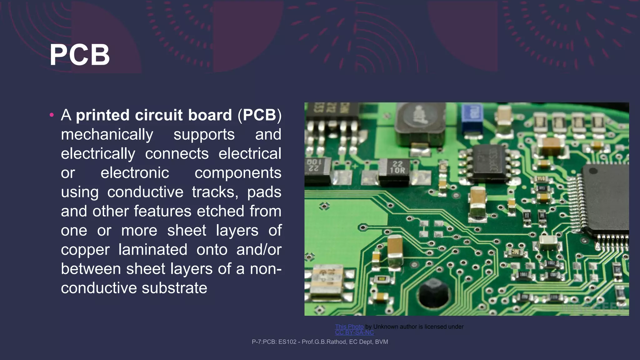
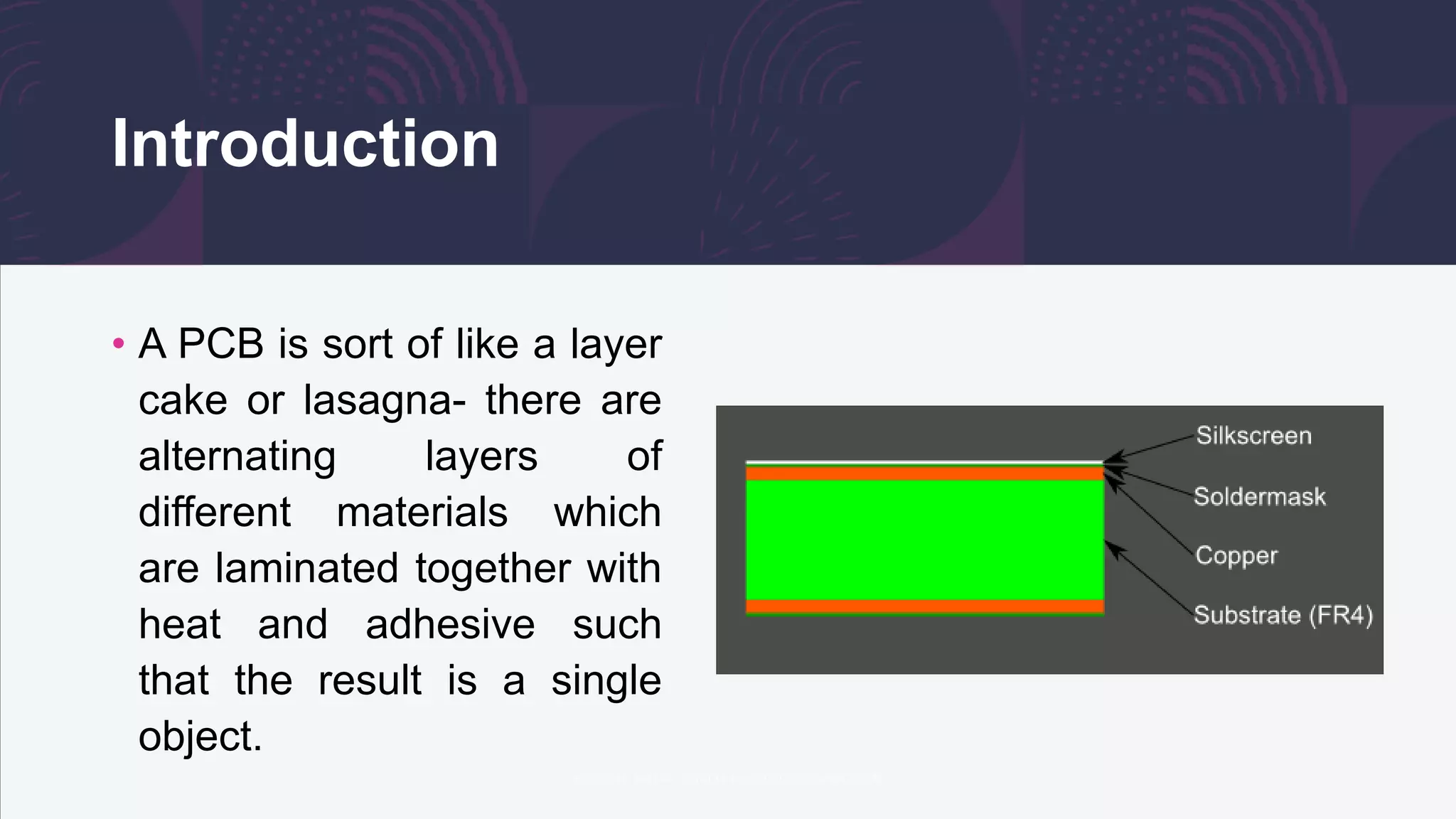
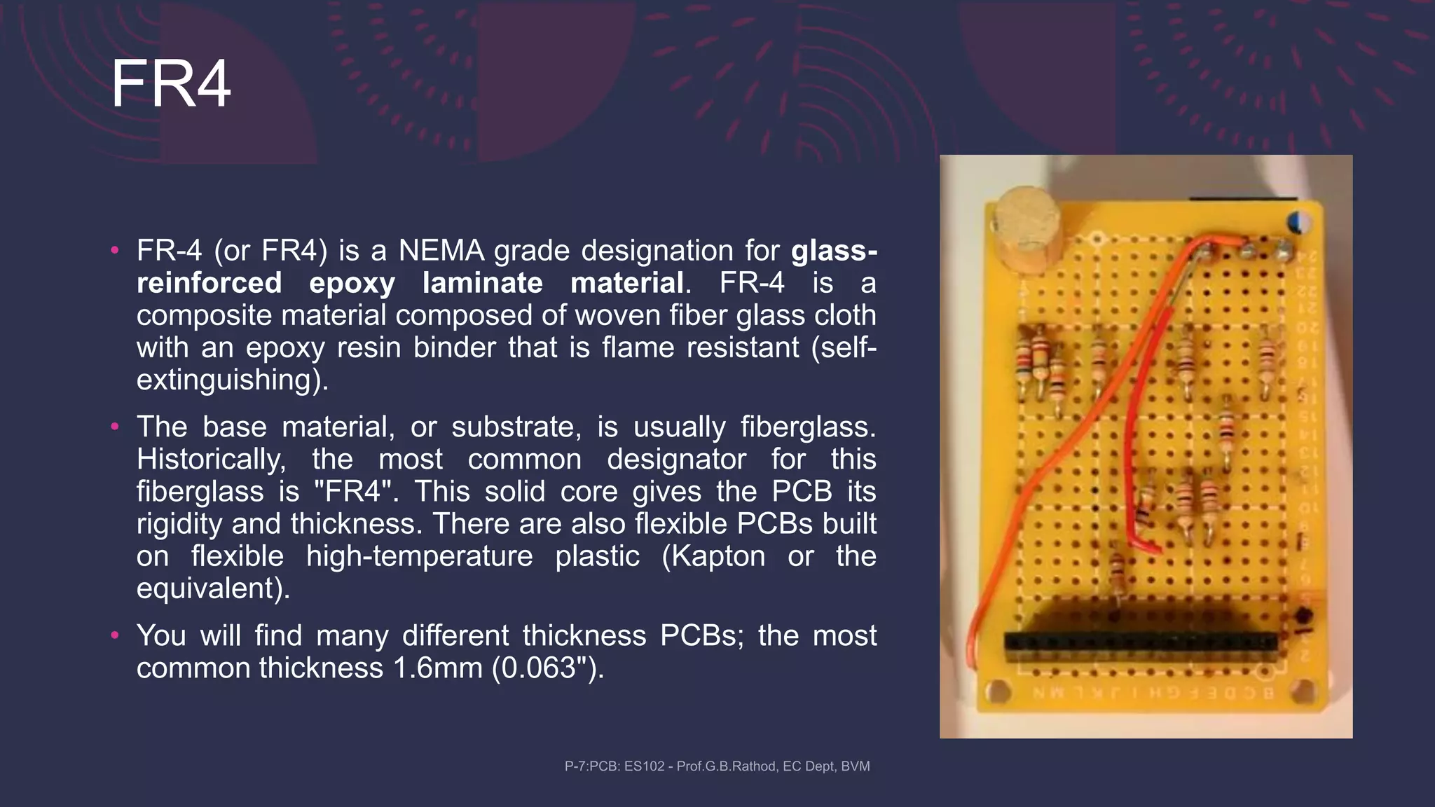
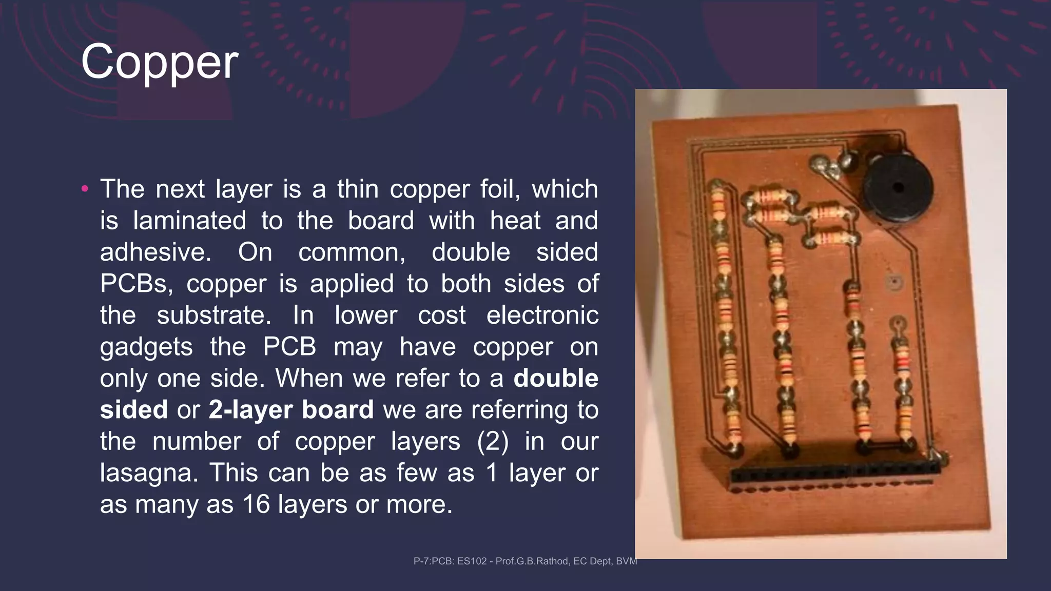
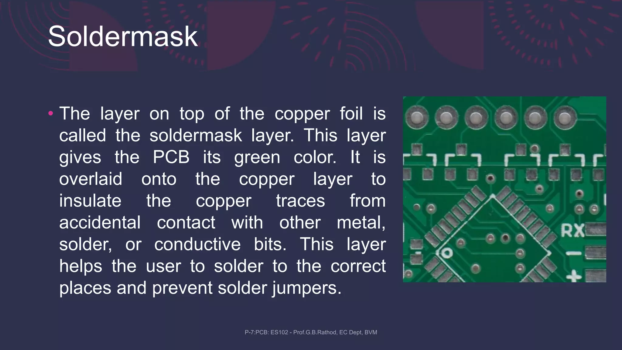
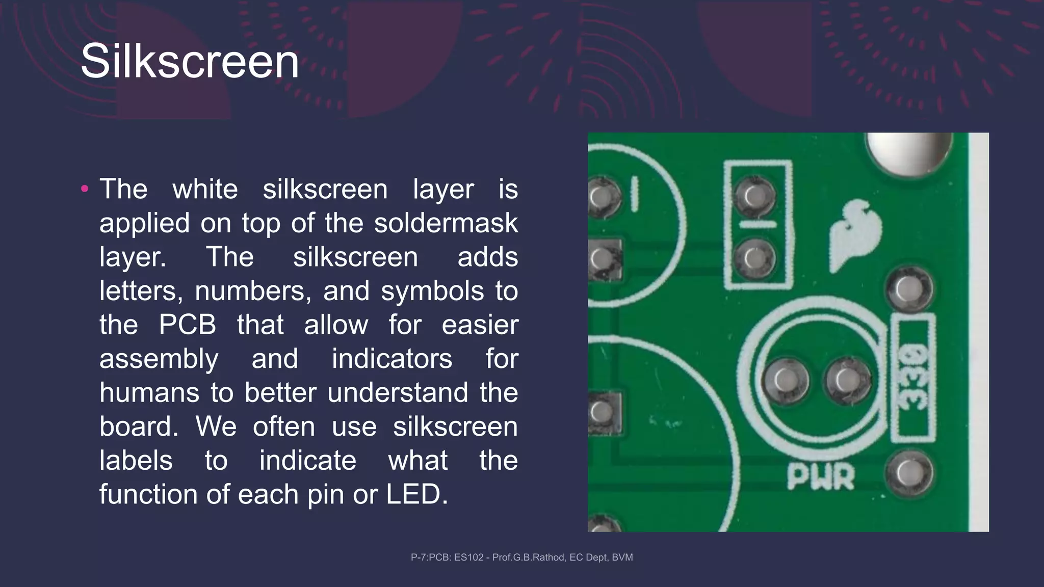
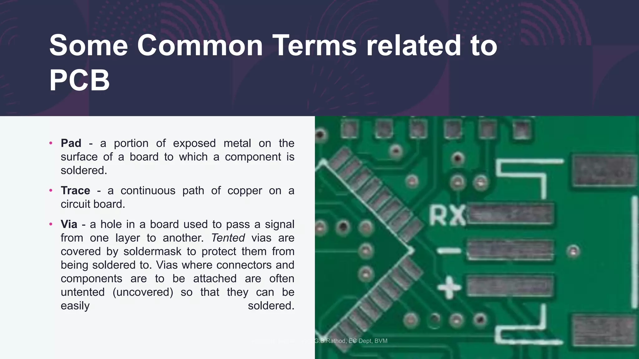
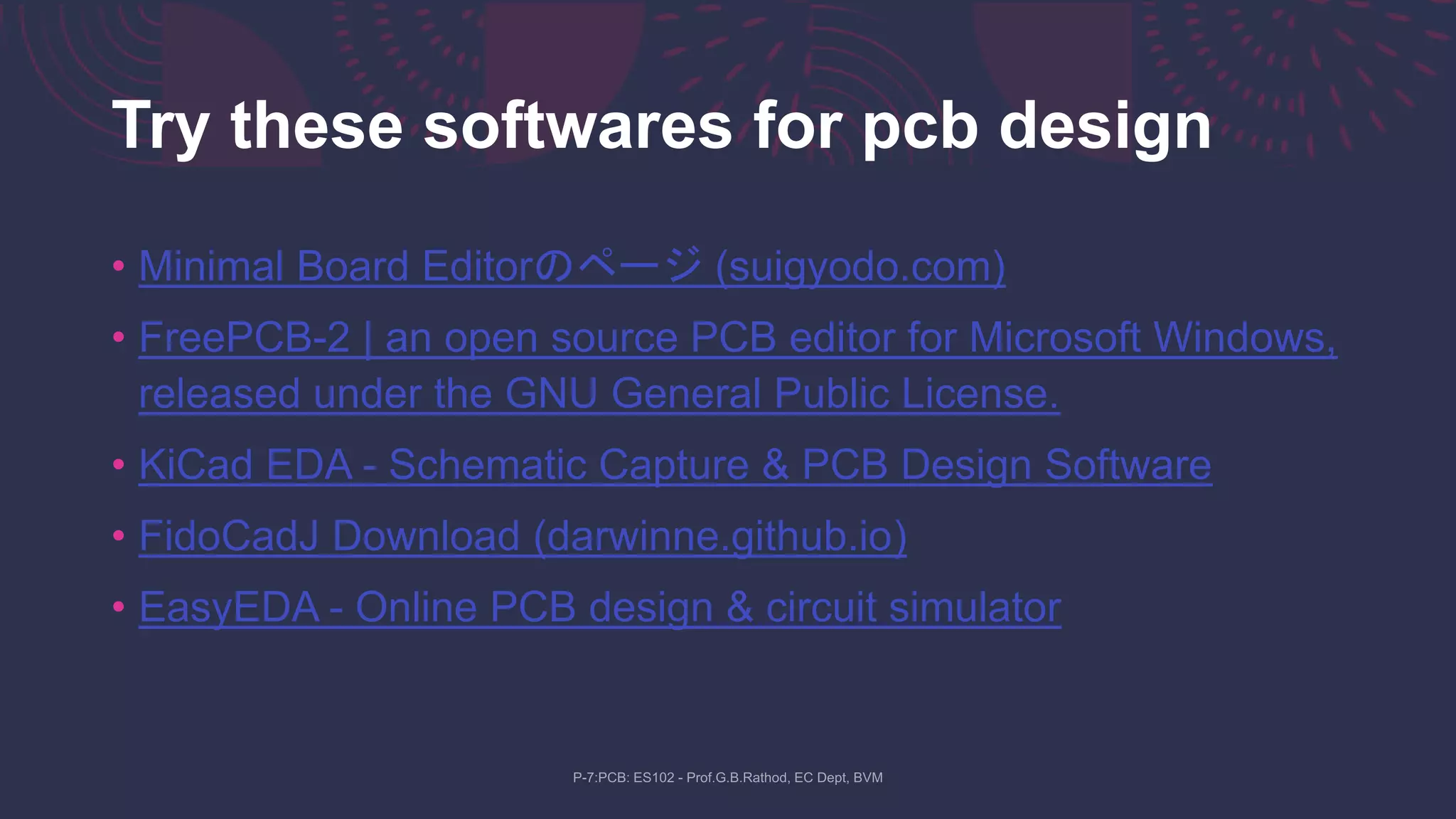


The document discusses the key components and layers that make up a printed circuit board (PCB). It explains that a PCB uses an insulating substrate like fiberglass, onto which are laminated thin copper layers for conductive traces. Additional layers include soldermask for insulation and silkscreen for labels. Common terms are also defined, like pads for component connections and vias for passing signals between layers. The document recommends some free and open-source PCB design software options.


