Download to read offline
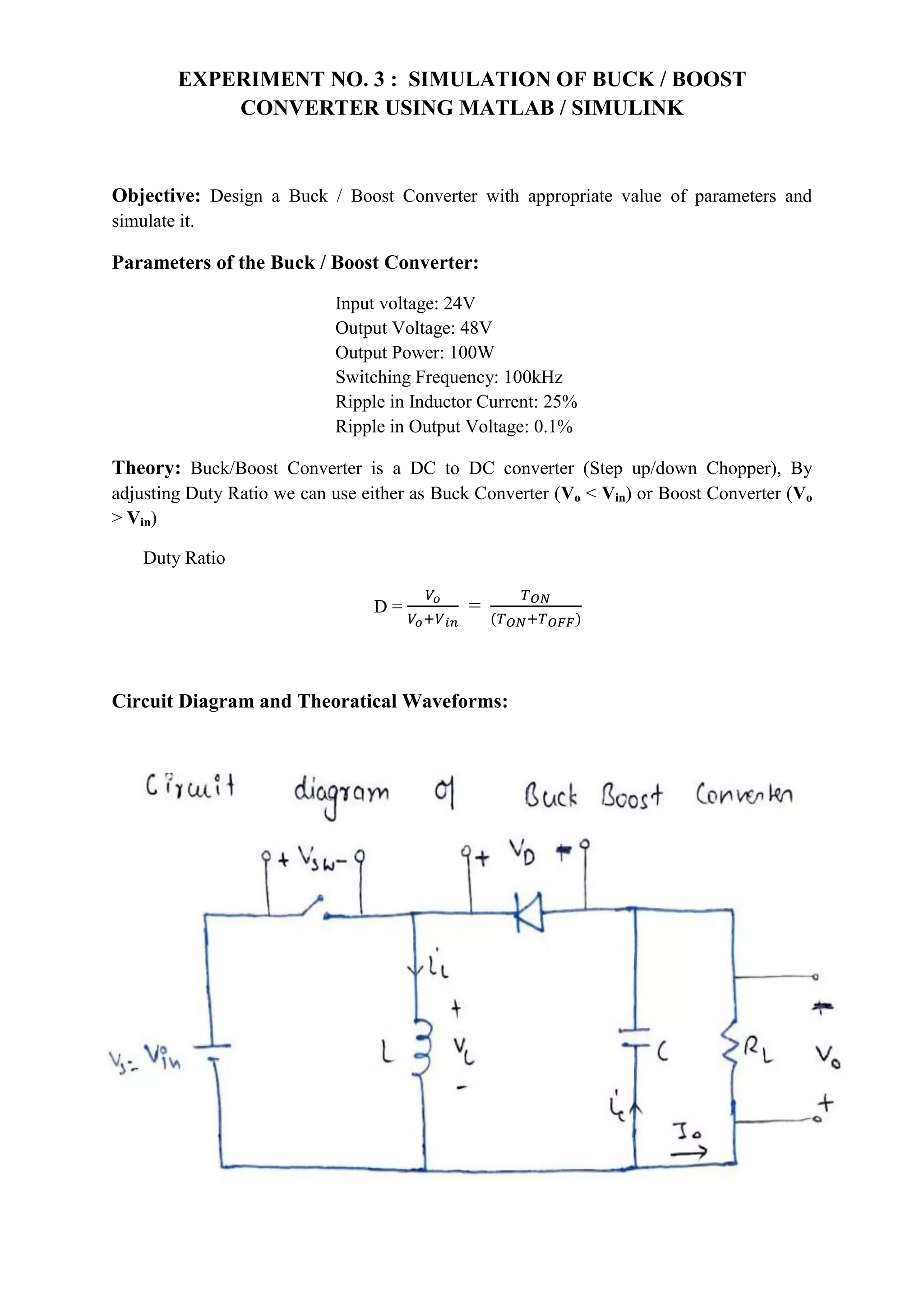
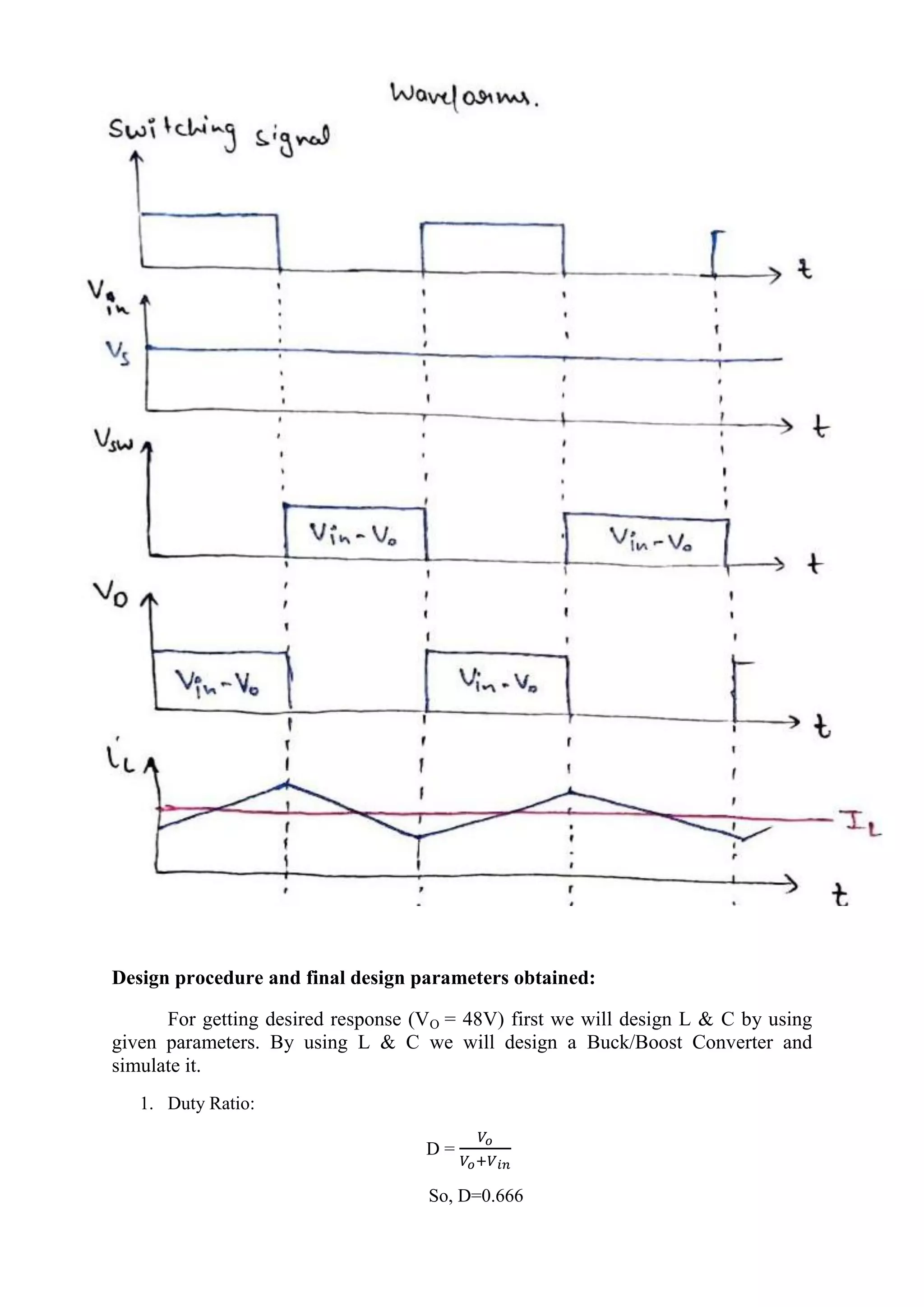
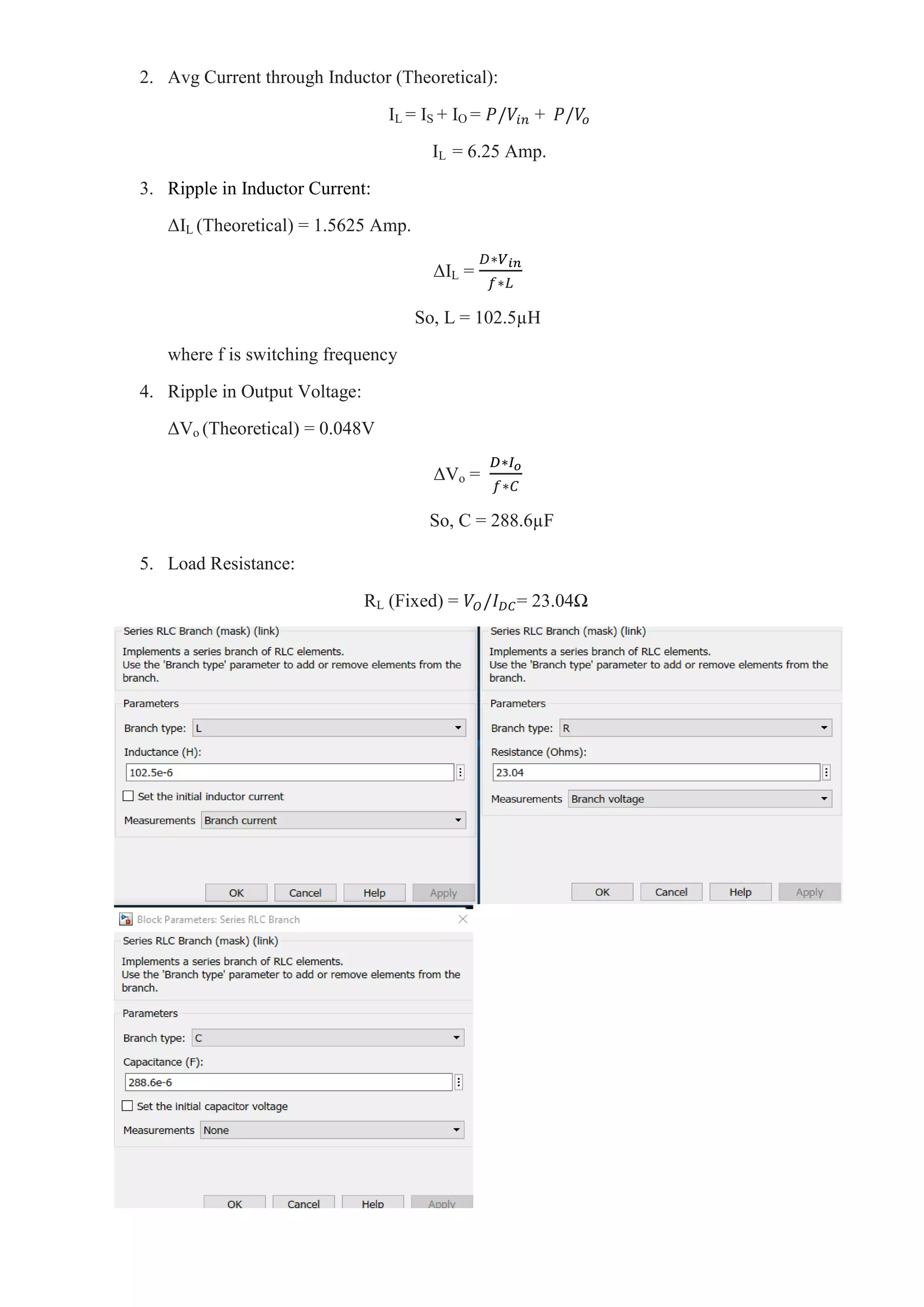
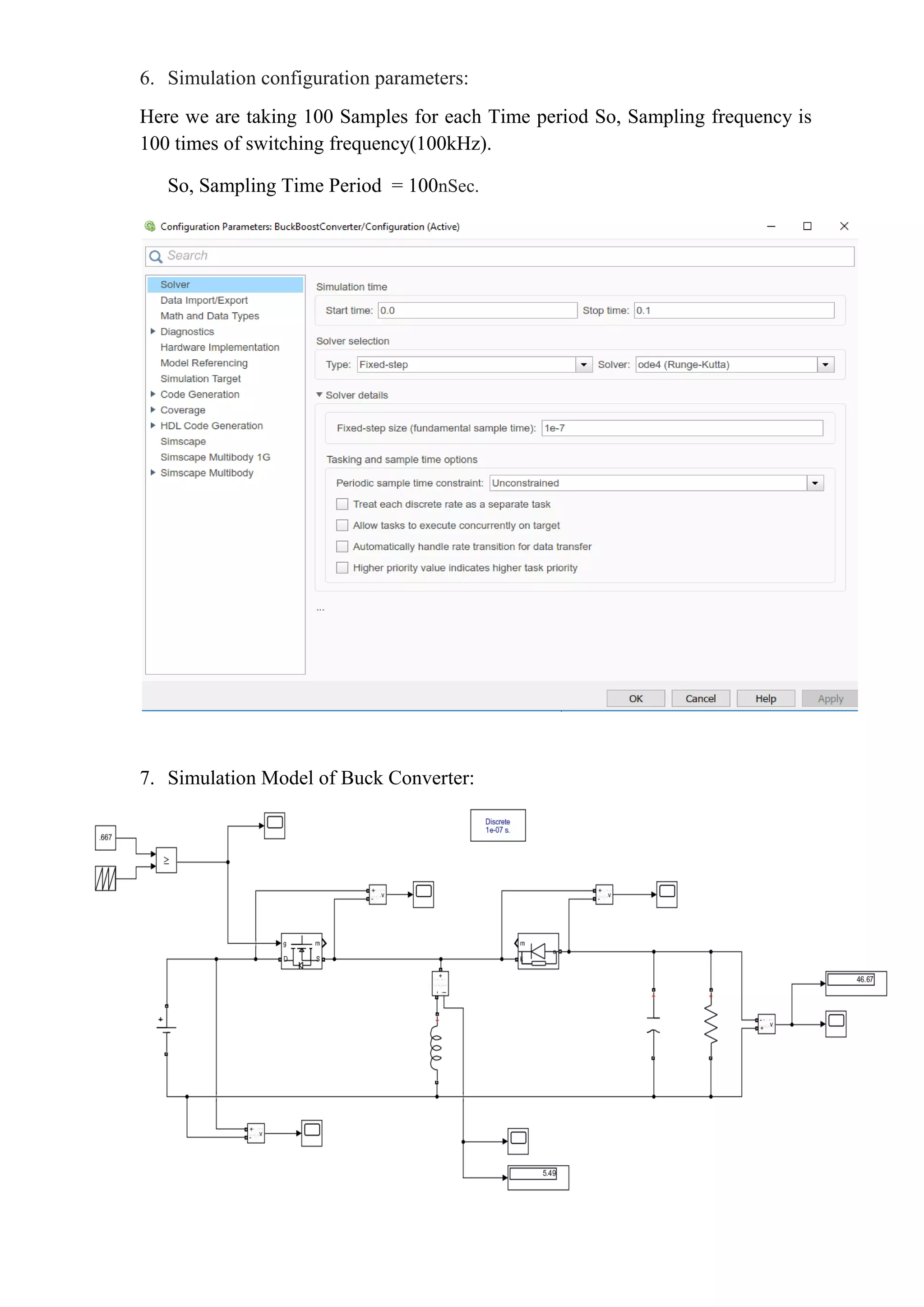
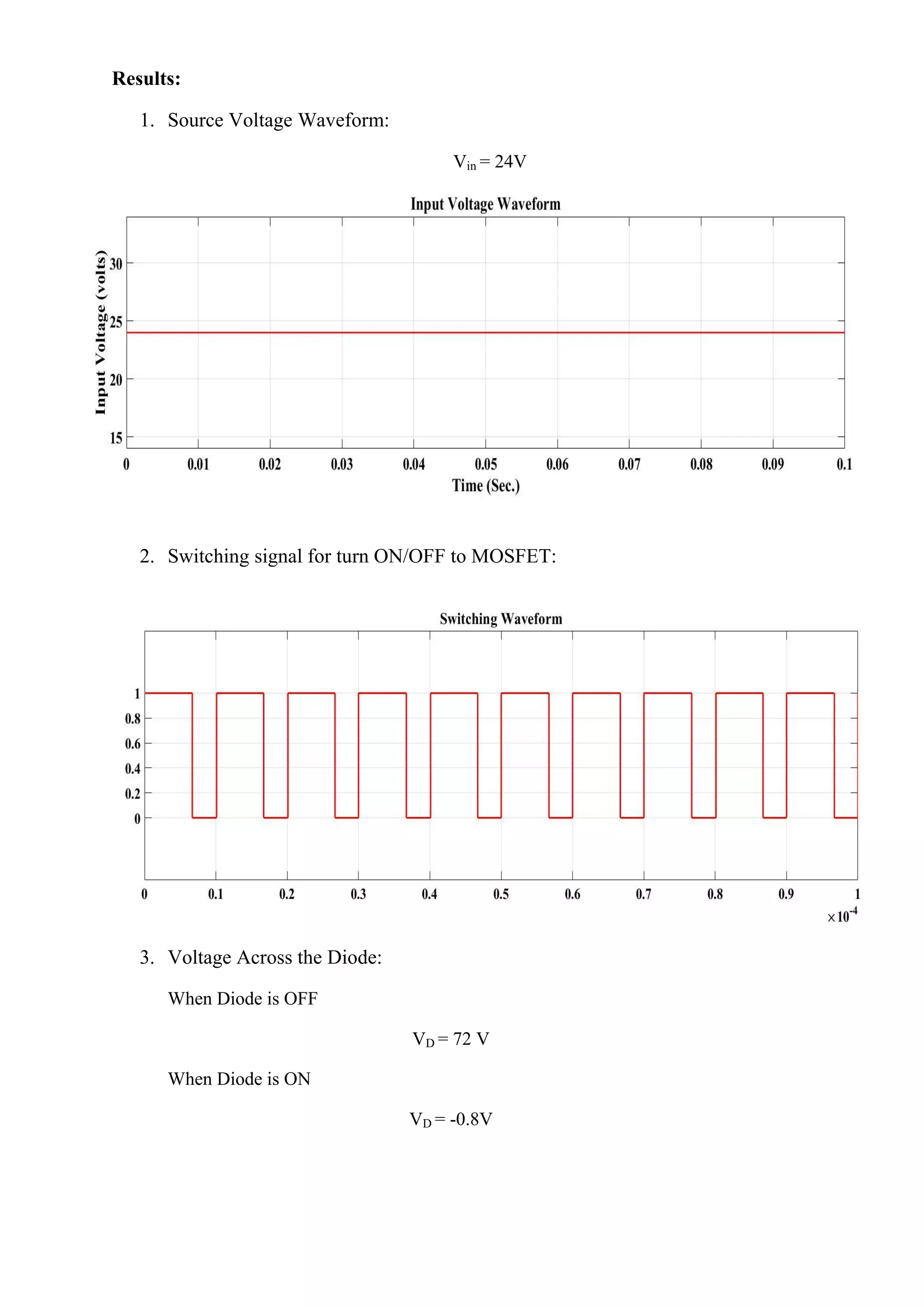


The document describes simulating a buck/boost converter using MATLAB/Simulink. It provides parameters for an input voltage of 24V, output voltage of 48V at 100W. It then outlines the theory, design procedure, and parameters calculated for an inductor value of 102.5μH and capacitor value of 288.6μF. The simulation model is shown and results presented including waveforms for the input voltage, switch signal, voltages across components, inductor current, and output voltage.