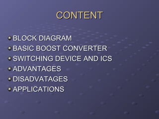
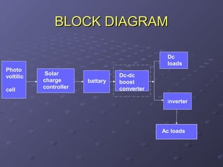
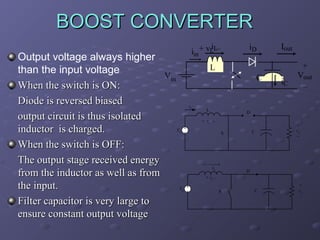
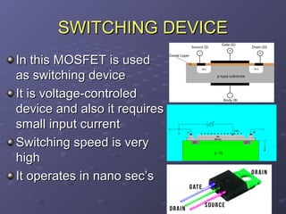
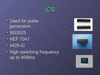
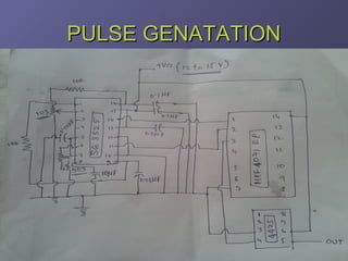
DC-DC BOOST CONVERTER
DESIGN FOR SOLAR
ELECTRIC SYSTEM

PRESENTED BY
V.SNEHA(10891A0203)
K.SWETHA(10891A0215)
V.SUDARSHAN(10891A0218)
CONTENT
BLOCK DIAGRAM
BASIC BOOST CONVERTER
SWITCHING DEVICE AND ICS
ADVANTAGES
DISADVATAGES
APPLICATIONS
BLOCK DIAGRAM
Dc
loads
Photo
voltilic
cell

Solar
charge
controller

battary

Dc-dc
boost
converter
inverter

Ac loads
BOOST CONVERTER
Output voltage always higher
than the input voltage
When the switch is ON:
Diode is reversed biased
output circuit is thus isolated
inductor is charged.
When the switch is OFF:
The output stage received energy
from the inductor as well as from
the input.
Filter capacitor is very large to
ensure constant output voltage

i
iin + vLLโ€“

iD

Iout

L

Vin

C

iL

L

iC

+
Vout
โ€“

D

+ vL โˆ’
Vd

C

S

iL

+
vo
โˆ’

D

+ vL Vd

S

C

+
vo
-
SWITCHING DEVICE
In this MOSFET is used
as switching device
It is voltage-controled
device and also it requires
small input current
Switching speed is very
high
It operates in nano secโ€™s
ICS
Used for pulse
genaration
SG3525
HEF 7041
4425 IC
High switching frequency
up to 400khz
PULSE GENATATION
ADVANTAGES
Only one switch
High effecience
Unidirectional output current
Provides one polarity output voltage
Low cost
Easy to analyze
Easy to understand
Simple circuit
DISADVANTAGES
Not sutable for high power conversion
Low amount of dc step up
Non isolated SMPS
APPLICATIONS
Commanly used as LED driver
Used for Solar power system
Used for Power factor corrections
Used in HVDC system
Applicable for LCDBACKLIGHTS &
FLASH LIGHTS
Used in HVE(Hybrid electric
vehicles)
ANY QUERIES
THANK YOU

Boost converter