Downloaded 211 times
![1.1) Input Waveform
- Simulation Result
Copyright (C) Siam Bee Technologies 2015 4
Time [sec]
VDC,AVG = 104.33V
VAC = 85Vrms
VDC, MIN = 85.8V](https://image.slidesharecdn.com/flybackconvertersimulatiomusingltspice-150702004230-lva1-app6892/75/Flyback-Converter-using-PWM-IC-LTspice-Version-4-2048.jpg)
![1.2) Output Waveform
- Simulation Result
Copyright (C) Siam Bee Technologies 2015 5
The output voltage is regulated at 12.12V
Time [sec]
The output current is 4.04A (RL=3)
V(Out) starts from 11V
by the initial condition](https://image.slidesharecdn.com/flybackconvertersimulatiomusingltspice-150702004230-lva1-app6892/75/Flyback-Converter-using-PWM-IC-LTspice-Version-5-2048.jpg)
![1.3) Output Power
- Simulation Result
Copyright (C) Siam Bee Technologies 2015 6
Time [sec]
The simulation result shows the output power is 48.90W](https://image.slidesharecdn.com/flybackconvertersimulatiomusingltspice-150702004230-lva1-app6892/75/Flyback-Converter-using-PWM-IC-LTspice-Version-6-2048.jpg)
![1.4) Gate Drive Output and Oscillator Timing (IC)
- Simulation Result
Copyright (C) Siam Bee Technologies 2015 7
Time [sec]
VOSC
Oscillator frequency = 105kHz
PW = 3.877us](https://image.slidesharecdn.com/flybackconvertersimulatiomusingltspice-150702004230-lva1-app6892/75/Flyback-Converter-using-PWM-IC-LTspice-Version-7-2048.jpg)

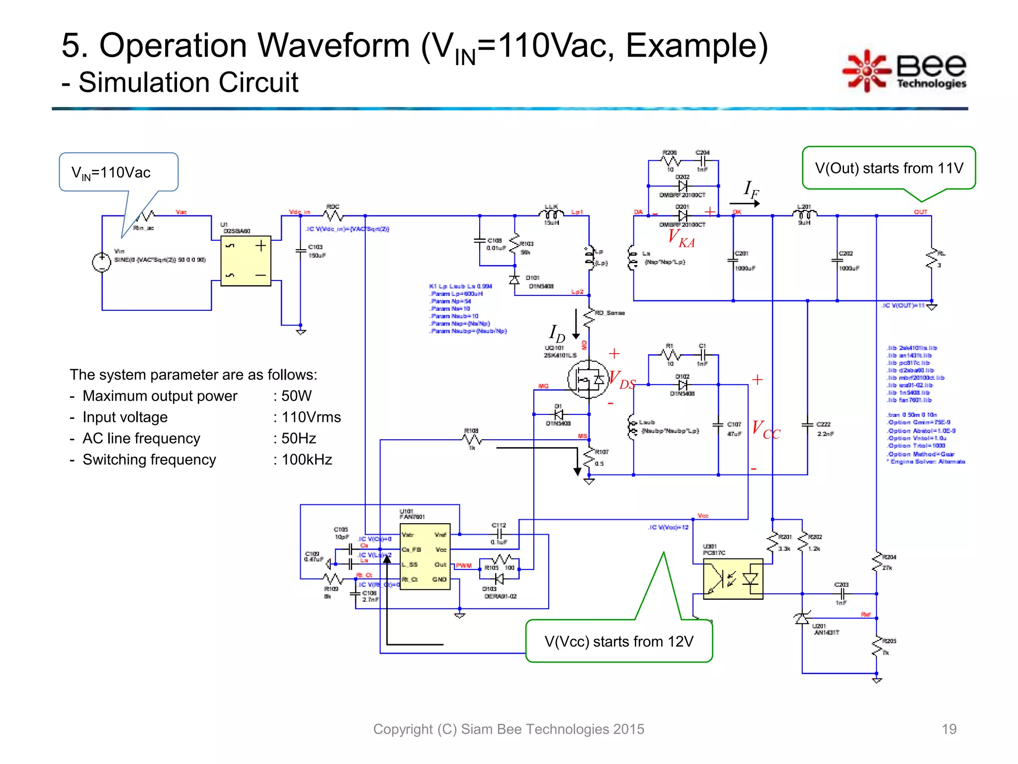
![2.1) Input Waveform
- Simulation Result
Copyright (C) Siam Bee Technologies 2015 9
Time [sec]
VDC,AVG = 142.41V
VAC = 110Vrms
VDC, MIN = 128.621V](https://image.slidesharecdn.com/flybackconvertersimulatiomusingltspice-150702004230-lva1-app6892/75/Flyback-Converter-using-PWM-IC-LTspice-Version-9-2048.jpg)
![2.2) Output Waveform
- Simulation Result
Copyright (C) Siam Bee Technologies 2015 10
The output voltage is regulated at 12.118V
Time [sec]
The output current is 4.039A (RL=3)
V(Out) starts from 11V
by the initial condition](https://image.slidesharecdn.com/flybackconvertersimulatiomusingltspice-150702004230-lva1-app6892/75/Flyback-Converter-using-PWM-IC-LTspice-Version-10-2048.jpg)
![2.3) Output Power
- Simulation Result
Copyright (C) Siam Bee Technologies 2015 11
Time [sec]
The simulation result shows the output power is 48.95W](https://image.slidesharecdn.com/flybackconvertersimulatiomusingltspice-150702004230-lva1-app6892/75/Flyback-Converter-using-PWM-IC-LTspice-Version-11-2048.jpg)
![2.4) Gate Drive Output and Oscillator Timing (IC)
- Simulation Result
Copyright (C) Siam Bee Technologies 2015 12
Time [sec]
PW = 3.282us
VOSC
Oscillator frequency = 105kHz](https://image.slidesharecdn.com/flybackconvertersimulatiomusingltspice-150702004230-lva1-app6892/75/Flyback-Converter-using-PWM-IC-LTspice-Version-12-2048.jpg)
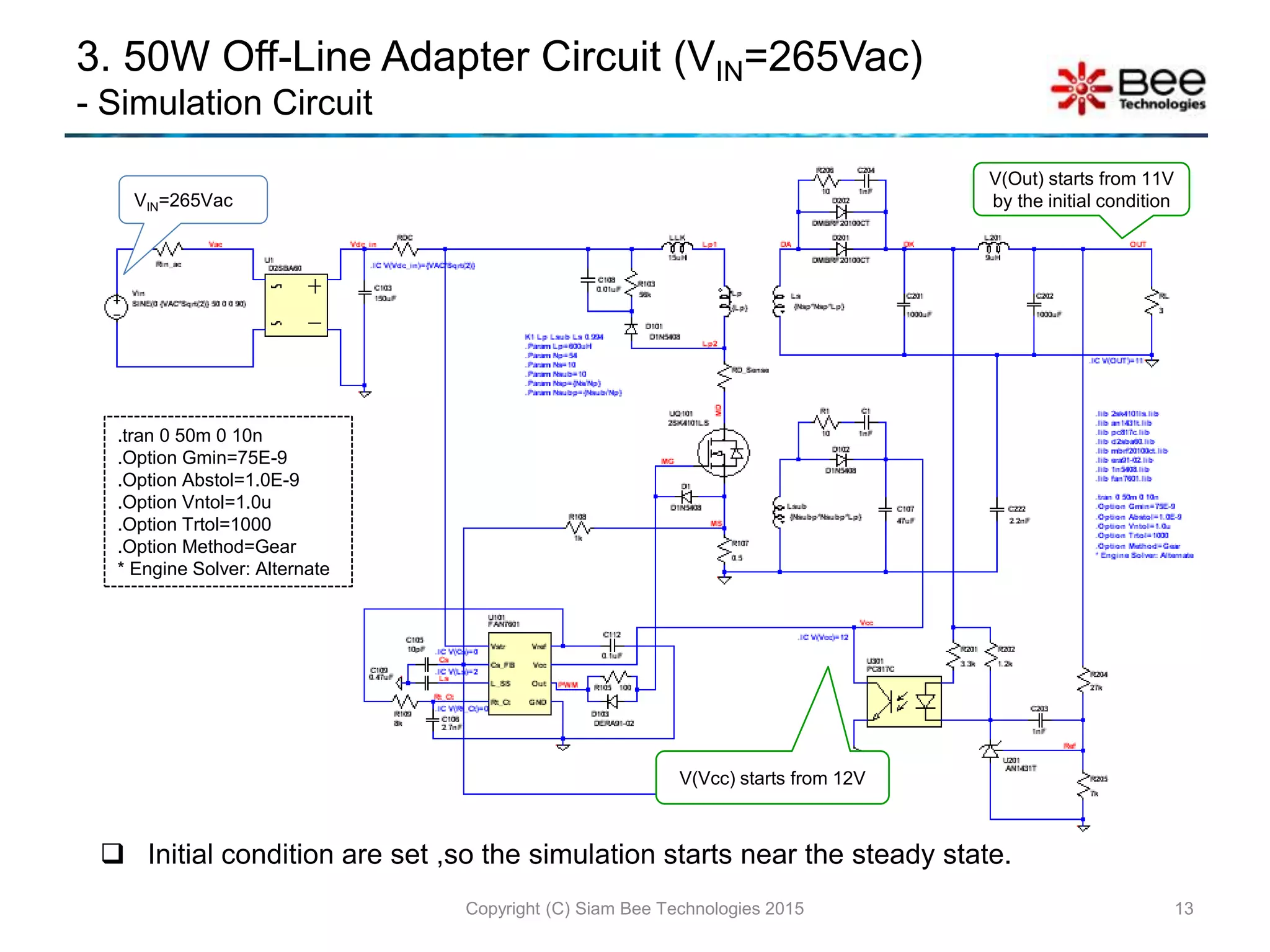
![3.1) Input Waveform
- Simulation Result
Copyright (C) Siam Bee Technologies 2015 14
Time [sec]
VDC,AVG = 367.58V
VAC = 265Vrms
VDC, MIN = 361.264V](https://image.slidesharecdn.com/flybackconvertersimulatiomusingltspice-150702004230-lva1-app6892/75/Flyback-Converter-using-PWM-IC-LTspice-Version-14-2048.jpg)
![3.2) Output Waveform
- Simulation Result
Copyright (C) Siam Bee Technologies 2015 15
The output voltage is regulated at 12.075V
Time [sec]
The output current is 4.025A (RL=3)
V(Out) starts from 11V
by the initial condition](https://image.slidesharecdn.com/flybackconvertersimulatiomusingltspice-150702004230-lva1-app6892/75/Flyback-Converter-using-PWM-IC-LTspice-Version-15-2048.jpg)
![3.3) Output Power
- Simulation Result
Copyright (C) Siam Bee Technologies 2015 16
Time [sec]
The simulation result shows the output power is 48.70W](https://image.slidesharecdn.com/flybackconvertersimulatiomusingltspice-150702004230-lva1-app6892/75/Flyback-Converter-using-PWM-IC-LTspice-Version-16-2048.jpg)
![3.4) Gate Drive Output and Oscillator Timing (IC)
- Simulation Result
Copyright (C) Siam Bee Technologies 2015 17
Time [sec]
PW = 1.706us
VOSC
Oscillator frequency = 105kHz](https://image.slidesharecdn.com/flybackconvertersimulatiomusingltspice-150702004230-lva1-app6892/75/Flyback-Converter-using-PWM-IC-LTspice-Version-17-2048.jpg)
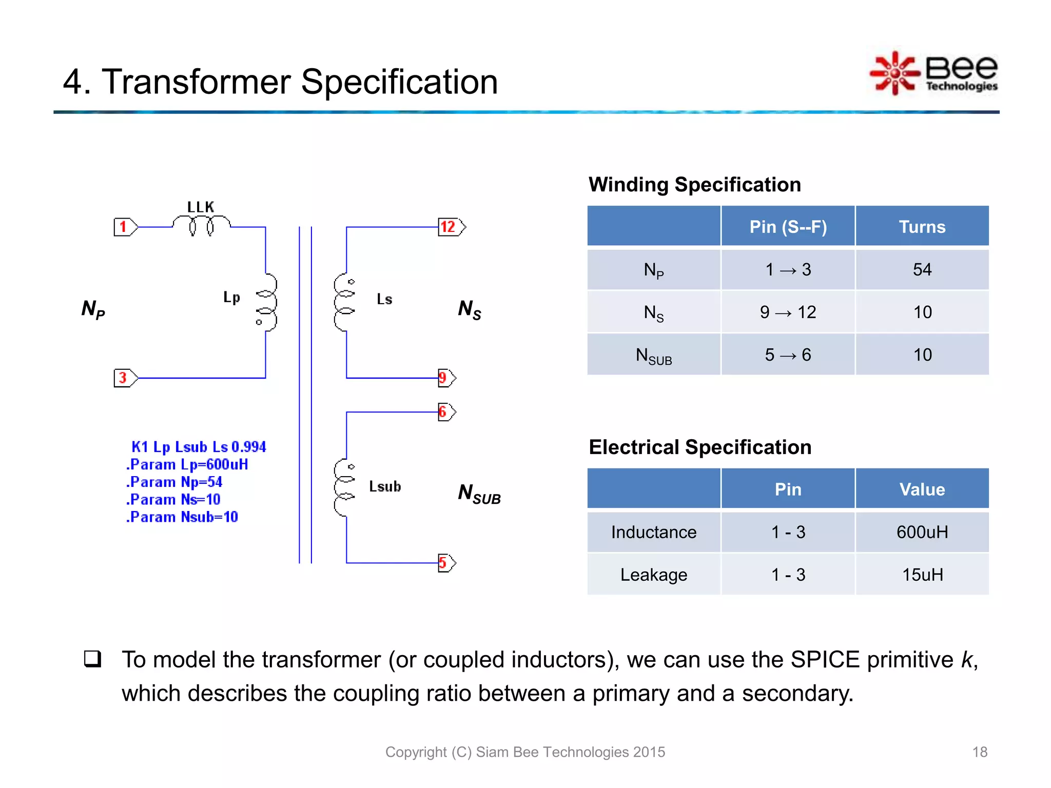
![5.1) Transformer Turn Ratio
- Simulation Result
Copyright (C) Siam Bee Technologies 2015 20
Time [sec]
VP
VS
VCC
This figure shows the waveforms of the voltages at each side of the transformer.](https://image.slidesharecdn.com/flybackconvertersimulatiomusingltspice-150702004230-lva1-app6892/75/Flyback-Converter-using-PWM-IC-LTspice-Version-20-2048.jpg)
![ This figure shows the waveforms of ID(UQ101) and IF(D201, D202) in the CCM mode.
The primary-side inductance (LP) of the transformer determines the converter operation mode.
5.2) Transformer Primary Side Inductance (LP)
- Simulation Result
Copyright (C) Siam Bee Technologies 2015 21
Time [sec]
ΟNΤ
Τ
IF(D201, D202)
VPWM
ID(UQ101)](https://image.slidesharecdn.com/flybackconvertersimulatiomusingltspice-150702004230-lva1-app6892/75/Flyback-Converter-using-PWM-IC-LTspice-Version-21-2048.jpg)
![5.3) VCC Output Waveform
- Simulation Result
Copyright (C) Siam Bee Technologies 2015 22
Time [sec]
VCC = 12.367V](https://image.slidesharecdn.com/flybackconvertersimulatiomusingltspice-150702004230-lva1-app6892/75/Flyback-Converter-using-PWM-IC-LTspice-Version-22-2048.jpg)
![5.4) MOSFET Switching Device (UQ101)
- Simulation Result
Copyright (C) Siam Bee Technologies 2015 23
Time [sec]
VDS(t)
ID(t)
Switching
loss (turn-off)
Switching loss
(turn-on)
Conduction loss
(VDS x ID)](https://image.slidesharecdn.com/flybackconvertersimulatiomusingltspice-150702004230-lva1-app6892/75/Flyback-Converter-using-PWM-IC-LTspice-Version-23-2048.jpg)
![5.5) Output Rectifier Diode (D201 - D202)
- Simulation Result
Copyright (C) Siam Bee Technologies 2015 24
Time [sec]
VKA(t) IF(t)
Peak magnitude
current
Conduction loss
(VF,AK x IF)
PLOSS_(D201, 202) (t)](https://image.slidesharecdn.com/flybackconvertersimulatiomusingltspice-150702004230-lva1-app6892/75/Flyback-Converter-using-PWM-IC-LTspice-Version-24-2048.jpg)
![5.6) Current Sensing and Feedback Circuit
- Simulation Result
Copyright (C) Siam Bee Technologies 2015 25
Time [sec]
1V Comparator
VCS](https://image.slidesharecdn.com/flybackconvertersimulatiomusingltspice-150702004230-lva1-app6892/75/Flyback-Converter-using-PWM-IC-LTspice-Version-25-2048.jpg)
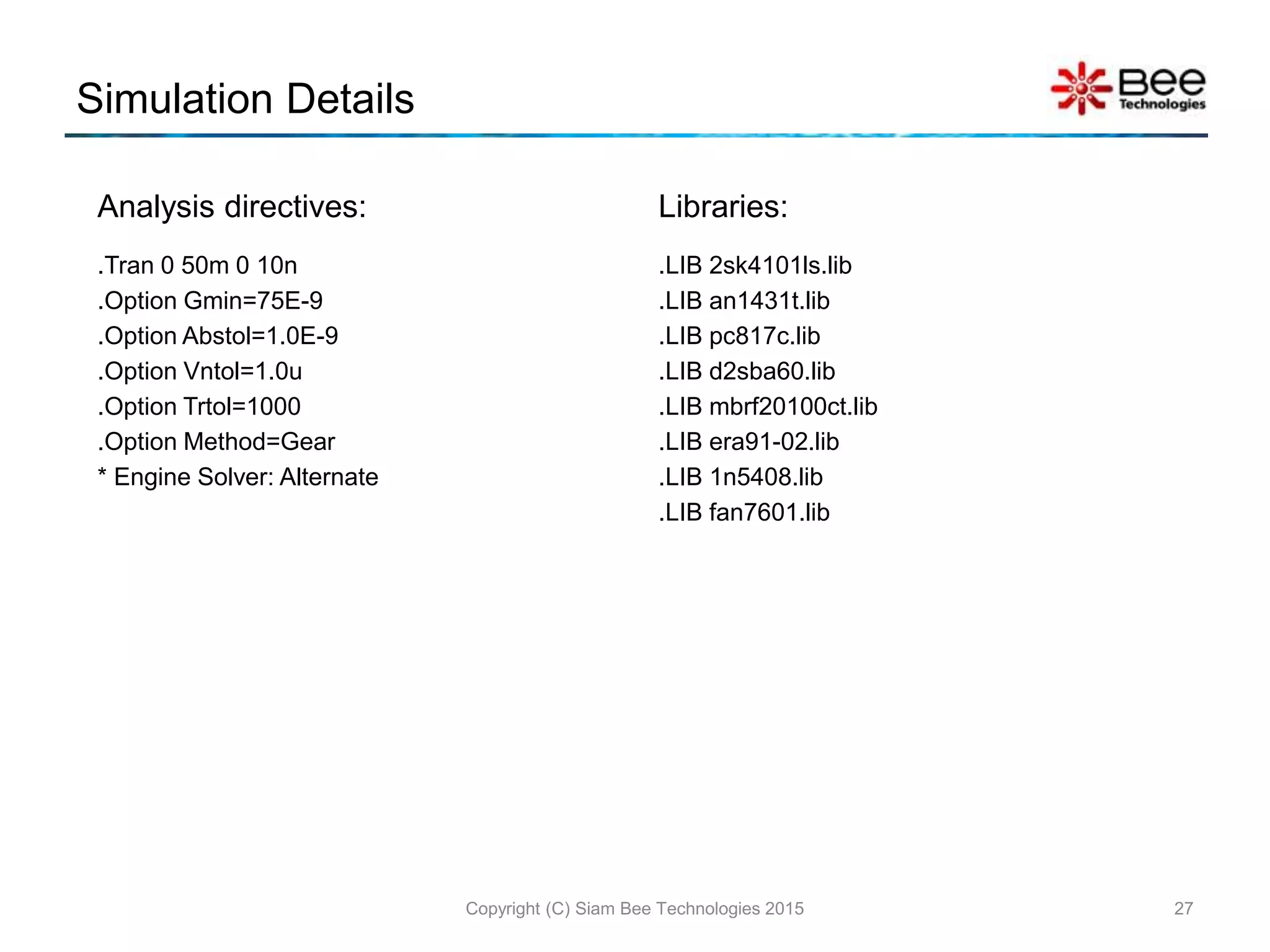
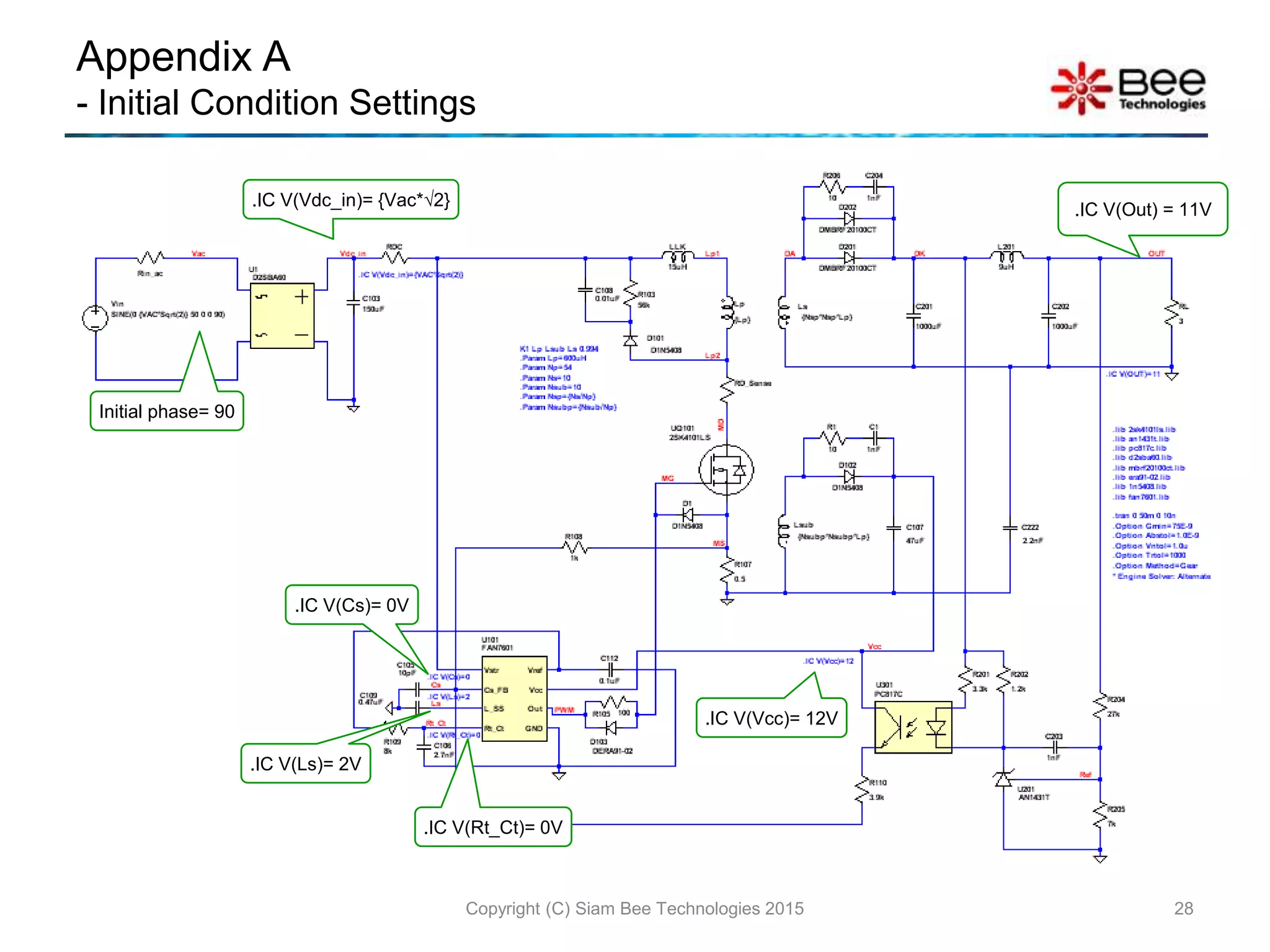
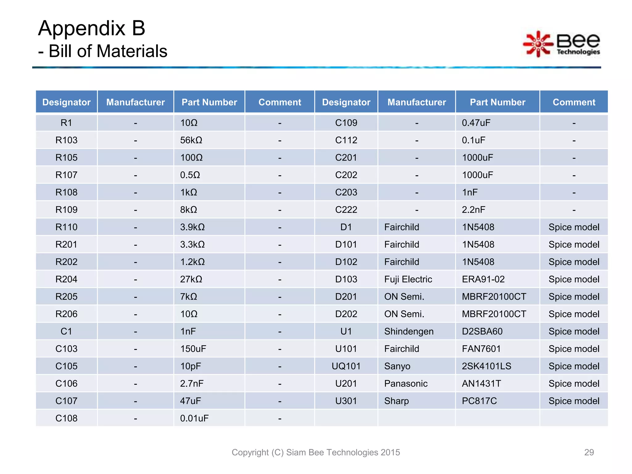
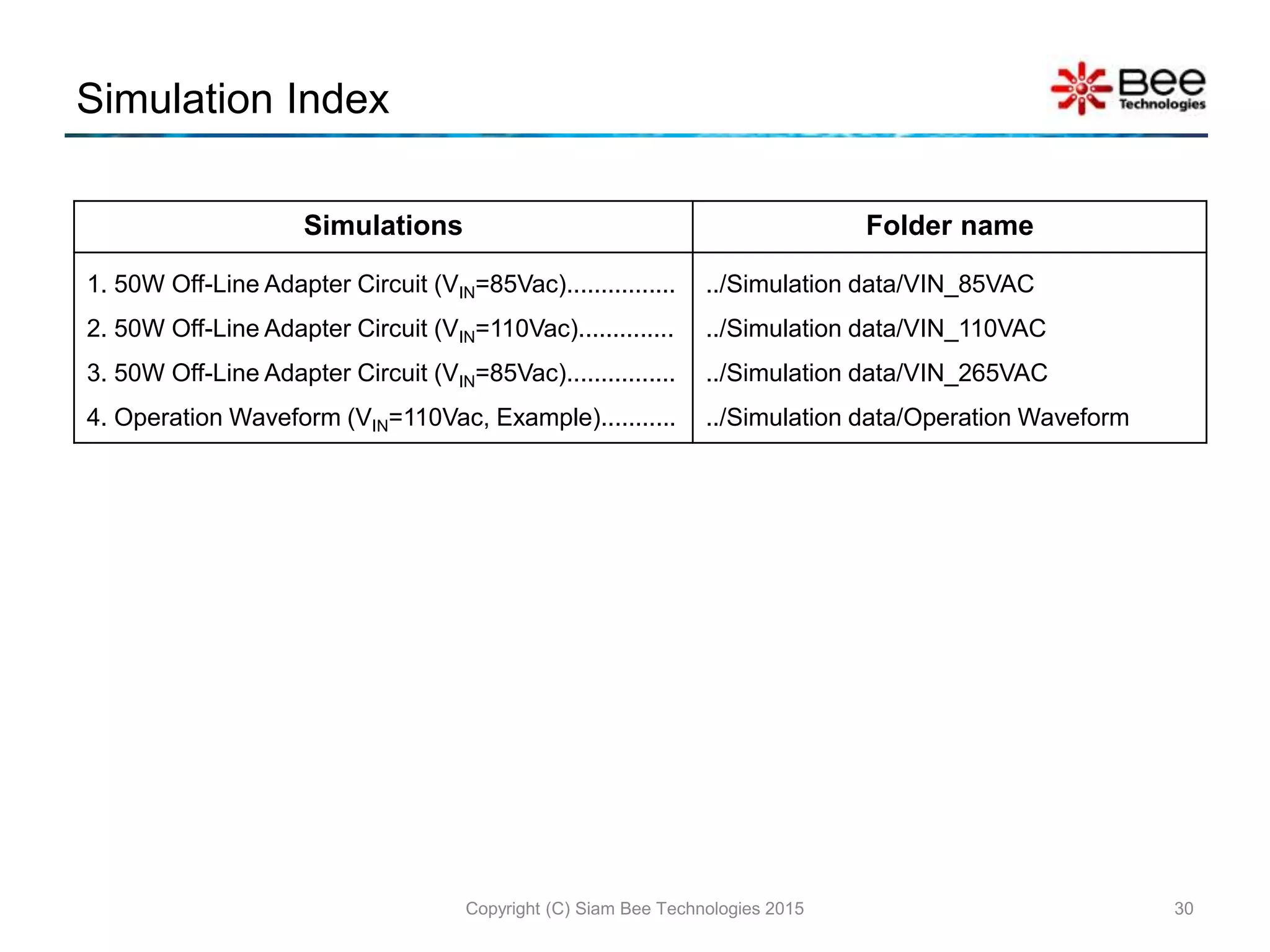

This document describes LTspice simulations of a 50W flyback converter circuit using different input voltages. It includes the circuit schematic, input and output waveforms, power output, and gate drive timing for input voltages of 85Vac, 110Vac and 265Vac. It also provides more detailed waveforms and analysis for an example simulation with 110Vac input, examining the transformer operation, MOSFET switching, and feedback circuit. Specifications and simulation settings are provided in appendices.
Introduction to Bee Technologies and outline of the 50W Off-Line Adapter Circuit overview.
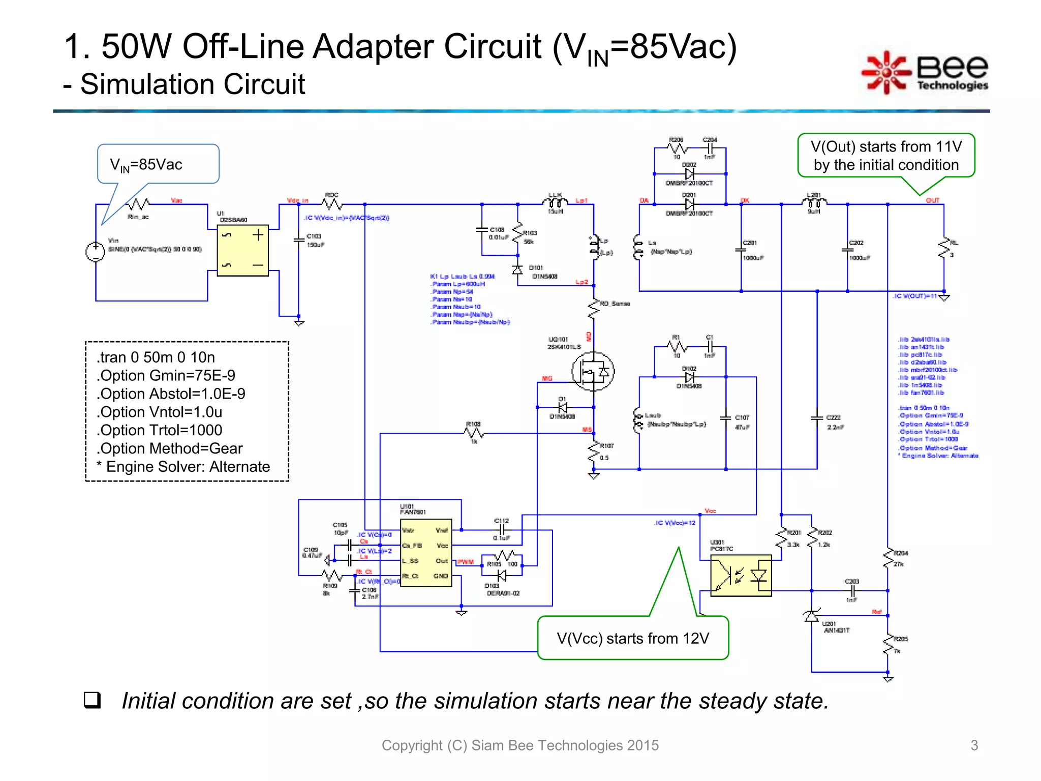
Detailed simulation of the 50W Off-Line Adapter Circuit with VIN=85Vac, including input/output waveforms, power output, and gate drive timing.
Simulation results for the 50W Off-Line Adapter Circuit at VIN=110Vac covering input/output analysis and power specifications.
Performance analysis for the 50W Off-Line Adapter Circuit with VIN=265Vac, including waveforms and power output.
Specifications of the transformer and operational waveform characteristics including current sensing and feedback circuit details.
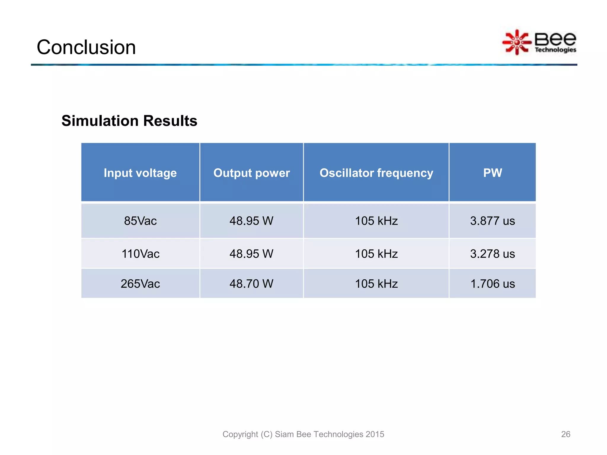
Summary table of simulation results for input voltages, output powers, and oscillation frequencies, along with additional simulation and material details.


![RF Module Design - [Chapter 5] Low Noise Amplifier](https://cdn.slidesharecdn.com/ss_thumbnails/rfch5-150613070346-lva1-app6891-thumbnail.jpg?width=640&height=640&fit=bounds)