Download to read offline
![Kommirisetti Bheema Raju. Int. Journal of Engineering Research and Application www.ijera.com
ISSN: 2248-9622, Vol. 7, Issue 1, (Part -1) January 2017, pp.87-90
www.ijera.com 87 | P a g e
Design And Verification of AMBA APB Protocol
1
Kommirisetti Bheema Raju,2
Bala Krishna Konda, M.Tech,
1
M.Tech Digital Electronics & Communication Systems(Decs) Student In Elure College Of Engineering And
Technology, Affiliated To Jntuk, Eluru, Andhra Pradesh.
2
Asistant Professor In The Department Of Ece In Eluru College Of Engineering And Technology, Affiliated To
Jntuk, Eluru, Andhra Pradesh
ABSTRACT:
Advanced microcontroller bus architecture (AMBA) is a well established open specification for the proper
management of functional blocks comprising system-on-chips (SOCs). A Memory Controller is designed to
cater to this problem. This design presents an intellectual property (IP) for inter-Advanced peripheral bus (APB)
protocol. The Memory Controller is a digital circuit which manages the flow of data going to and from the main
memory. It can be a separate chip or can be integrated into the system chipset. This paper revolves around
building an Advanced Microcontroller Bus Architecture (AMBA) compliant Memory Controller as an
Advanced High-performance Bus (AHB) slave. The work involved is of APB Protocol and its slave
Verification. The whole design is captured using VHDL, simulated with ModelSim and configured to a FPGA
target device belonging to the Virtex4 family using Xilinx.
I. INTRODUCTION
In the realm of processing, these elements
perform different tasks in order to realize an overall
solution. Consider a set-top box for television (TV)
sets as an example [1]. A set-top box must generate
inputs for a particular television channel from the
received digital satellite signal. The entire process
incorporates several phases. The first is to split the
incoming digital signal into its component video and
audio data streams. The next phase is to convert the
video data stream into its actual television signal.
Also, the audio data stream has to be changed into
audio signal for the TV set. Besides, an additional job
to look after will be to handle the user input for
changing the channel when the remote control will be
pressed. All these operations have to be completed
not only simultaneously but within a certain time
frame. The cost of not accomplishing these within the
stipulated time frame or deadline will be manifested
in the form of blank screen or audible noises. This is
obviously unacceptable and hence, it is necessary to
always deliver the data within real-time deadlines.
The needed computational elements here will be
either general-purpose or special-purpose processors
(such as signal processors). Nowadays, multitudes of
these devices are integrated in the form of an SOC. A
processor needs to interact with other processors,
memories or input/output (I/O) devices to complete a
task. Currently, bus systems are used to interconnect
the intellectual property (IP) blocks.
Many SoCs comprise Application Specific
Integrated Circuits (ASICs) that are offered by
several companies. The Advanced RISC Machines
(ARM) microprocessor is very popular for SoC
solutions. Today it is fair to say that the ARM
Embedded Technology is universally recognized as
an industry standard for ASIC design for portable
applications. Creating and applying powerful,
portable and at the same time re-usable intellectual
Property (IP), capable of enhancing an ARM core is
therefore of utmost importance to any ASIC design
centre.
Description Of Amba Ahb Bus.
An AMBA AHB design may include one or
more bus masters, typically a system would contain
at least the processor and the test interface . However,
it would also be common for a Direct Memory
Access (DMA) or Digital Signal Processor (DSP) to
be included as bus masters. The external memory
interface, the Advanced Peripheral Bus (APB) Bridge
and any internal memory are the most common AHB
slaves. Any other peripheral in the system could also
be included as an AHB slave. However, low-
bandwidth peripherals typically reside on the APB.
Fig. 1 A typical AMBA architecture.
Before an AMBA AHB transfer can
commence the bus master must be granted access to
the bus. This process is started by the master
RESEARCH ARTICLE OPEN ACCESS](https://image.slidesharecdn.com/o0701018790-170124053903/75/Design-And-Verification-of-AMBA-APB-Protocol-1-2048.jpg)
![Kommirisetti Bheema Raju. Int. Journal of Engineering Research and Application www.ijera.com
ISSN: 2248-9622, Vol. 7, Issue 1, (Part -1) January 2017, pp.87-90
www.ijera.com 89 | P a g e
Fig6: RTL Schematic diagram of APB Master Slave
Burst.
Write cycle
At T1, a write transfer starts with PADDR,
PWDATA, PWRITE, and PSEL, being registered at
the rising edge of PCLK. It is called the SETUP
cycle. At the next rising edge of the clock T2 it is
called ACCESS cycle, PENABLE, and PREADY,
are registered. When asserted, PENABLE indicates
starting of Access phase of the transfer. When
asserted, PREADY indicates that the slave can
complete the transfer at the next rising edge of
PCLK. The PADDR, PWDATA, and control signals
all remain valid until the transfer completes at T3, the
end of the Access phase. The PENABLE, is disabled
at the end of the transfer. The select signal PSEL is
also disabled unless the transfer is to be followed
immediately by another transfer to the same
peripheral.
Fig 4: APB Write cycle.
Read cycle
During read operation the PENABLE,
PSEL, PADDR PWRITE, signals are asserted at the
clock edge T1 (SETUP cycle). At the clock edge T2,
(ACCESS cycle), the PENABLE, PREADY are
asserted and PRDATA is also read during this phase.
The slave must provide the data before the end of the
read transfer.
Fig 5: APB Read Cycle.
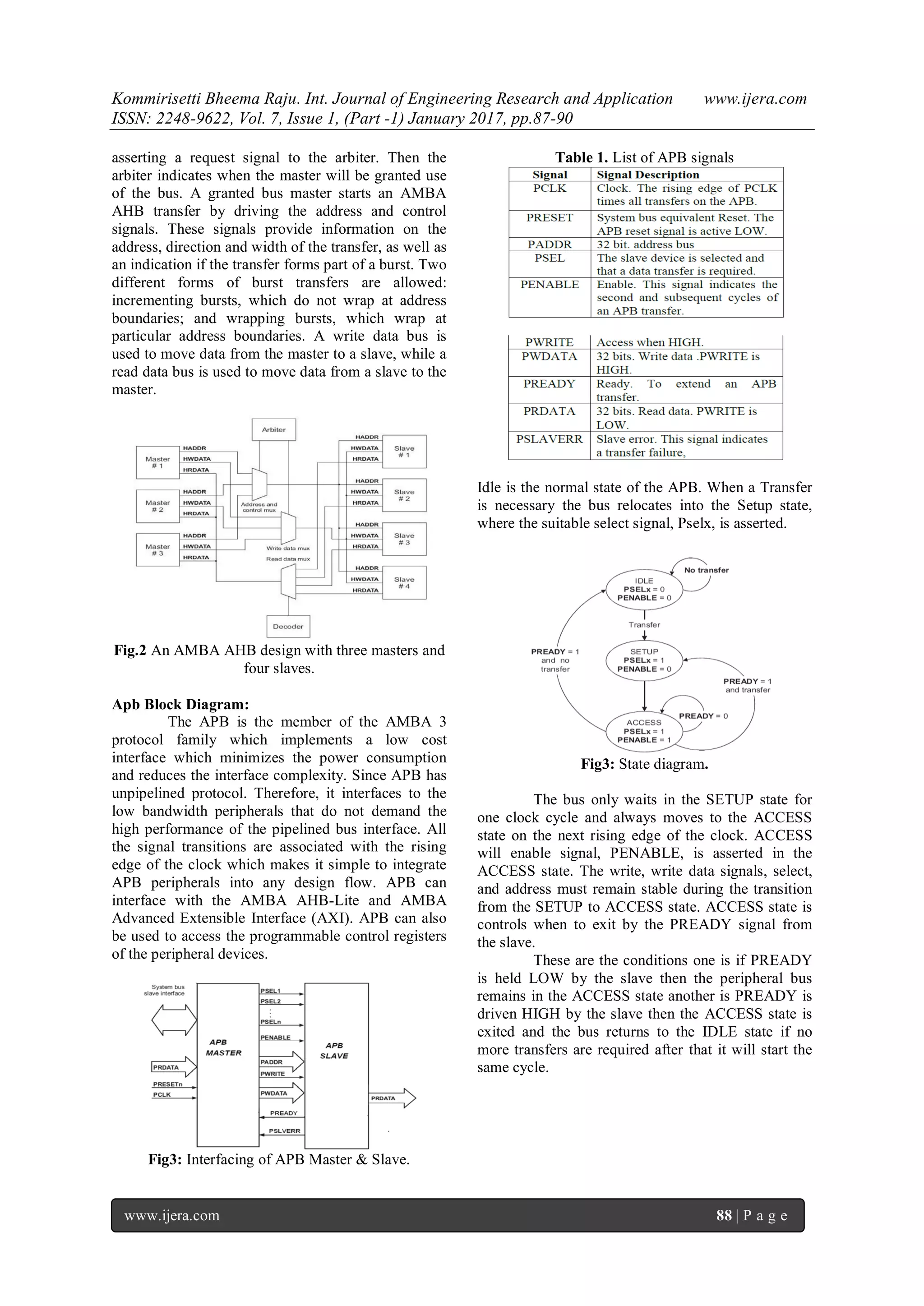
Simulation Results
Fig6: simulation result for amba apb master slave
burst.
II. CONCLUSION
This paper gives an outline of the AMBA
bus architecture and explains the APB bus in detail.
The design has taken care of balance between area
overhead and speed. The read write operation is
accomplished with zero wait states from the external
ROM and the write operation with zero states to the
external RAM. The APB bus is designed using the
Verilog HDL according to the specification and is
verified using Xilinx.
REFERENCES
[1]. “Design and Implementation of High-
Performance Master/Slave Memory Controller
with Microcontroller Bus Architecture”
Shashisekhar Ramagundam1, Sunil R.Das1, 2,
Scott Morton1, Satyendra N. Biswas4, Voicu
Groza2, Mansour H. Assaf3, and Emil M.
Petriu2 1Department of Computer Science,
College of Arts and Sciences, Troy University,
Montgomery, AL 36103, USA School of
Information Technology and Engineering,
Faculty of Engineering, University of Ottawa,
Ottawa, ON K1N 6N5, Canada 3School of
Engineering and Physics, University of the
South Pacific, Suva 19128, Fiji 4School of
Engineering and Technology, Kaziranga
University, Jorhat 785006, India.
[2]. Y. Hu and B. Yang, “Building an AMBA
AHB compliant memory controller”,
Proceedings of the Third International
Conference on Measuring Technology and
Mechatronics Automation, Vol. 01, 2011, pp.
658–661.
[3]. S. Rao and A. S. Phadke, “Implementation of
AMBA compliant memory controller on a
FPGA”, International Journal of Emerging
Trends in Electrical and Electronics, Vol. 2,
April 2013, pp. 20–23.
[4]. AMBA Specification (Rev 2.0), ARM Inc.,
1999.
[5]. AHB Example – AMBA System, Technical
Reference Manual, ARM Inc., 1999.
[6]. Sudeep Pasricha, “On-Chip Communication
Architecture Synthesis for Multi-Processor](https://image.slidesharecdn.com/o0701018790-170124053903/75/Design-And-Verification-of-AMBA-APB-Protocol-3-2048.jpg)
![Kommirisetti Bheema Raju. Int. Journal of Engineering Research and Application www.ijera.com
ISSN: 2248-9622, Vol. 7, Issue 1, (Part -1) January 2017, pp.87-90
www.ijera.com 90 | P a g e
Systems-on-Chip”, University of California,
2008.
[7]. “PrimeCell Synchronous Static Memory
Controller”, Technical Reference Manual,
ARM Inc, 2001-2005.
[8]. URL:http://wwwmicro.deis.unibo.it/~magagni
/amba99.pdf
[9]. ARM, “AMBA Specification Overview”,
available at http://www.arm.com/.
[10]. ARM, “AMBA Specification (Rev 2.0)”,
available at http://www.arm.com.
[11]. URL:http://www.differencebetween.net/techno
logy/difference-between-ahb-and-apb
[12]. Samir Palnitkar, “Verilog HDL: A guide to
Digital Design and Synthesis (2nd Edition),
Pearson, 2008.
[13]. URL:http://www.testbench.com.
Bala Krishna Konda is currently working
as an Asst. Prof. in the Department of ECE
in Eluru College of Engineering and
Technology. He completed his B.Tech in
ECE from Sri Vasavi Engineering College,
Tadepalligudem, Andhra Pradesh and
M.Tech from Sri Vasavi Engineering
College, Tadepalligudem, Andhra Pradesh.
He is interested in the field of VLSI.
Kommirisetti Bheema Raju has obtained
his Graduation at Akula Gopayya College
of Engineering, Tadepalligudem, Andhara
Pradesh and currently pursuing his Post
Graduation From Eluru College of
Engineering and Technology, Eluru,
Andhra Pradesh.](https://image.slidesharecdn.com/o0701018790-170124053903/75/Design-And-Verification-of-AMBA-APB-Protocol-4-2048.jpg)

The document discusses the design and verification of an Advanced Microcontroller Bus Architecture (AMBA) compliant memory controller, focusing on the Advanced Peripheral Bus (APB) protocol. It details the design process, including the use of VHDL for the implementation and simulation with ModelSim, as well as verification on FPGA hardware. The paper emphasizes the balance between area efficiency and speed in realizing the APB interface for low-bandwidth peripherals.