#1 Lecture slides prepared for “Computer Organization and Architecture”, 10/e, by William Stallings, Chapter 5 “Internal Memory”.
#2 We begin this chapter with a survey of semiconductor main memory subsystems,
including ROM, DRAM, and SRAM memories. Then we look at error control
techniques used to enhance memory reliability. Following this, we look at more
advanced DRAM architectures.
#3 In earlier computers, the most common form of random-access storage for computer
main memory employed an array of doughnut-shaped ferromagnetic loops
referred to as cores. Hence, main memory was often referred to as core, a term that
persists to this day. The advent of, and advantages of, microelectronics has long
since vanquished the magnetic core memory. Today, the use of semiconductor chips
for main memory is almost universal. Key aspects of this technology are explored
in this section.
The basic element of a semiconductor memory is the memory cell. Although a variety
of electronic technologies are used, all semiconductor memory cells share certain
properties:
• They exhibit two stable (or semistable) states, which can be used to represent
binary 1 and 0.
• They are capable of being written into (at least once), to set the state.
• They are capable of being read to sense the state.
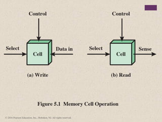
Figure 5.1 depicts the operation of a memory cell. Most commonly, the cell
has three functional terminals capable of carrying an electrical signal. The select
terminal, as the name suggests, selects a memory cell for a read or write operation.
The control terminal indicates read or write. For writing, the other terminal
provides an electrical signal that sets the state of the cell to 1 or 0. For reading, that
terminal is used for output of the cell’s state. The details of the internal organization,
functioning, and timing of the memory cell depend on the specific integrated
circuit technology used and are beyond the scope of this book, except for a brief
summary. For our purposes, we will take it as given that individual cells can be
selected for reading and writing operations.
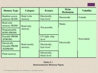
#4 All of the memory types that we will explore in this chapter are random access. That is,
individual words of memory are directly accessed through wired-in addressing logic.
Table 5.1 lists the major types of semiconductor memory. The most common
is referred to as random-access memory (RAM). This is, in fact, a misuse of the
term, because all of the types listed in the table are random access. One distinguishing
characteristic of memory that is designated as RAM is that it is possible
both to read data from the memory and to write new data into the memory easily
and rapidly. Both the reading and writing are accomplished through the use of
electrical signals.
The other distinguishing characteristic of RAM is that it is volatile. A RAM
must be provided with a constant power supply. If the power is interrupted, then
the data are lost. Thus, RAM can be used only as temporary storage. The two traditional
forms of RAM used in computers are DRAM and SRAM.
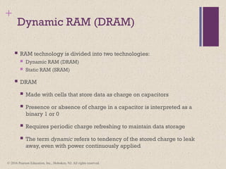
#5 RAM technology is divided into two technologies: dynamic and
static. A dynamic RAM (DRAM) is made with cells that store data as charge on
capacitors. The presence or absence of charge in a capacitor is interpreted as a
binary 1 or 0. Because capacitors have a natural tendency to discharge, dynamic
RAMs require periodic charge refreshing to maintain data storage. The term
dynamic refers to this tendency of the stored charge to leak away, even with power
continuously applied.
#6 Figure 5.2a is a typical DRAM structure for an individual cell that stores 1 bit.
The address line is activated when the bit value from this cell is to be read or written.
The transistor acts as a switch that is closed (allowing current to flow) if a voltage is
applied to the address line and open (no current flows) if no voltage is present on
the address line.
For the write operation, a voltage signal is applied to the bit line; a high voltage
represents 1, and a low voltage represents 0. A signal is then applied to the
address line, allowing a charge to be transferred to the capacitor.
For the read operation, when the address line is selected, the transistor turns
on and the charge stored on the capacitor is fed out onto a bit line and to a sense
amplifier. The sense amplifier compares the capacitor voltage to a reference value
and determines if the cell contains a logic 1 or a logic 0. The readout from the cell
discharges the capacitor, which must be restored to complete the operation.
Although the DRAM cell is used to store a single bit (0 or 1), it is essentially
an analog device. The capacitor can store any charge value within a range; a threshold
value determines whether the charge is interpreted as 1 or 0.
Figure 5.2b is a typical SRAM structure for an individual cell. Four transistors
(T1, T2, T3, T4) are cross connected in an arrangement that produces a stable logic
state. In logic state 1, point C1 is high and point C2 is low; in this state, T1 and T4 are off
and T2 and T3 are on. In logic state 0, point C1 is low and point C2 is high; in this state,
T1 and T4 are on and T2 and T3 are off. Both states are stable as long as the direct
current (dc) voltage is applied. Unlike the DRAM, no refresh is needed to retain data.
As in the DRAM, the SRAM address line is used to open or close a switch.
The address line controls two transistors (T5 and T6). When a signal is applied to
this line, the two transistors are switched on, allowing a read or write operation. For
a write operation, the desired bit value is applied to line B, while its complement
is applied to line B. This forces the four transistors (T1, T2, T3, T4) into the proper
state. For a read operation, the bit value is read from line B.
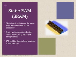
#7 In contrast, a static RAM (SRAM) is a digital device that uses the
same logic elements used in the processor. In a SRAM, binary values are stored
using traditional flip-flop logic-gate configurations (see Chapter 11 for a description
of flip-flops). A static RAM will hold its data as long as power is supplied to it.
As in the DRAM, the SRAM address line is used to open or close a switch.
The address line controls two transistors (T5 and T6 ). When a signal is applied to
this line, the two transistors are switched on, allowing a read or write operation. For
a write operation, the desired bit value is applied to line B, while its complement
is applied to line B. This forces the four transistors (T1 , T2 , T3 , T4 ) into the proper
state. For a read operation, the bit value is read from line B.
#8 Both static and dynamic RAMs are volatile; that is,
power must be continuously supplied to the memory to preserve the bit values.
A dynamic memory cell is simpler and smaller than a static memory cell. Thus, a
DRAM is more dense (smaller cells = more cells per unit area) and less expensive
than a corresponding SRAM. On the other hand, a DRAM requires the supporting
refresh circuitry. For larger memories, the fixed cost of the refresh circuitry is more
than compensated for by the smaller variable cost of DRAM cells. Thus, DRAMs
tend to be favored for large memory requirements. A final point is that SRAMs are
somewhat faster than DRAMs. Because of these relative characteristics, SRAM is
used for cache memory (both on and off chip), and DRAM is used for main memory.
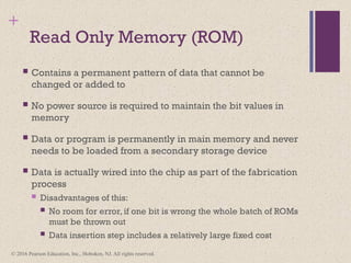
#9 As the name suggests, a read-only memory (ROM) contains a permanent pattern
of data that cannot be changed. A ROM is nonvolatile; that is, no power source is
required to maintain the bit values in memory. While it is possible to read a ROM,
it is not possible to write new data into it. An important application of ROMs is
microprogramming, discussed in Part Four. Other potential applications include
• Library subroutines for frequently wanted functions
• System programs
• Function tables
For a modest-sized requirement, the advantage of ROM is that the data or program
is permanently in main memory and need never be loaded from a secondary storage
device.
A ROM is created like any other integrated circuit chip, with the data actually
wired into the chip as part of the fabrication process. This presents two problems:
• The data insertion step includes a relatively large fixed cost, whether one or
thousands of copies of a particular ROM are fabricated.
• There is no room for error. If one bit is wrong, the whole batch of ROMs must
be thrown out.
#10 When only a small number of ROMs with a particular memory content is
needed, a less expensive alternative is the programmable ROM (PROM). Like the
ROM, the PROM is nonvolatile and may be written into only once. For the PROM,
the writing process is performed electrically and may be performed by a supplier
or customer at a time later than the original chip fabrication. Special equipment is
required for the writing or “programming” process. PROMs provide flexibility and
convenience. The ROM remains attractive for high-volume production runs.
#11 Another variation on read-only memory is the read-mostly memory, which is
useful for applications in which read operations are far more frequent than write
operations but for which nonvolatile storage is required. There are three common
forms of read-mostly memory: EPROM, EEPROM, and flash memory.
The optically erasable programmable read-only memory (EPROM) is read
and written electrically, as with PROM. However, before a write operation, all the
storage cells must be erased to the same initial state by exposure of the packaged
chip to ultraviolet radiation. Erasure is performed by shining an intense ultraviolet
light through a window that is designed into the memory chip. This erasure process
can be performed repeatedly; each erasure can take as much as 20 minutes to
perform. Thus, the EPROM can be altered multiple times and, like the ROM and
PROM, holds its data virtually indefinitely. For comparable amounts of storage, the
EPROM is more expensive than PROM, but it has the advantage of the multiple
update capability.
A more attractive form of read-mostly memory is electrically erasable programmable
read-only memory (EEPROM). This is a read-mostly memory that can
be written into at any time without erasing prior contents; only the byte or bytes
addressed are updated. The write operation takes considerably longer than the read
operation, on the order of several hundred microseconds per byte. The EEPROM
combines the advantage of non-volatility with the flexibility of being updatable in
place, using ordinary bus control, address, and data lines. EEPROM is more expensive
than EPROM and also is less dense, supporting fewer bits per chip.
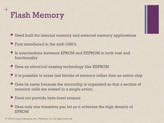
Another form of semiconductor memory is flash memory (so named because
of the speed with which it can be reprogrammed). First introduced in the mid-1980s,
flash memory is intermediate between EPROM and EEPROM in both cost and
functionality. Like EEPROM, flash memory uses an electrical erasing technology.
An entire flash memory can be erased in one or a few seconds, which is much faster
than EPROM. In addition, it is possible to erase just blocks of memory rather than
an entire chip. Flash memory gets its name because the microchip is organized so
that a section of memory cells are erased in a single action or “flash.” However,
flash memory does not provide byte-level erasure. Like EPROM, flash memory
uses only one transistor per bit, and so achieves the high density (compared with
EEPROM) of EPROM.
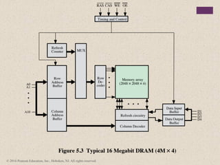
#12 Figure 5.3 shows a typical organization of a 16-Mbit DRAM. In this case, 4 bits
are read or written at a time. Logically, the memory array is organized as four square
arrays of 2048 by 2048 elements. Various physical arrangements are possible. In any
case, the elements of the array are connected by both horizontal (row) and vertical
(column) lines. Each horizontal line connects to the Select terminal of each cell in its
row; each vertical line connects to the Data-In/Sense terminal of each cell in its column.
Address lines supply the address of the word to be selected. A total of log2 W
lines are needed. In our example, 11 address lines are needed to select one of 2048
rows. These 11 lines are fed into a row decoder, which has 11 lines of input and 2048
lines for output. The logic of the decoder activates a single one of the 2048 outputs
depending on the bit pattern on the 11 input lines (211 = 2048).
An additional 11 address lines select one of 2048 columns of 4 bits per column.
Four data lines are used for the input and output of 4 bits to and from a data buffer.
On input (write), the bit driver of each bit line is activated for a 1 or 0 according to
the value of the corresponding data line. On output (read), the value of each bit line
is passed through a sense amplifier and presented to the data lines. The row line
selects which row of cells is used for reading or writing.
Because only 4 bits are read/written to this DRAM, there must be multiple
DRAMs connected to the memory controller to read/write a word of data to the bus.
Note that there are only 11 address lines (A0–A10), half the number you
would expect for a 2048 * 2048 array. This is done to save on the number of pins.
The 22 required address lines are passed through select logic external to the chip
and multiplexed onto the 11 address lines. First, 11 address signals are passed to the
chip to define the row address of the array, and then the other 11 address signals are
presented for the column address.
As an aside, multiplexed addressing plus the use of square arrays result in a
quadrupling of memory size with each new generation of memory chips. One more
pin devoted to addressing doubles the number of rows and columns, and so the size
of the chip memory grows by a factor of 4.
Figure 5.3 also indicates the inclusion of refresh circuitry. All DRAMs require
a refresh operation. A simple technique for refreshing is, in effect, to disable the
DRAM chip while all data cells are refreshed. The refresh counter steps through all
of the row values. For each row, the output lines from the refresh counter are supplied
to the row decoder and the RAS line is activated. The data are read out and
written back into the same location. This causes each cell in the row to be refreshed.
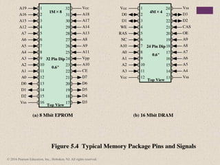
#13 As was mentioned in Chapter 2, an integrated circuit is mounted on a package that
contains pins for connection to the outside world.
Figure 5.4a shows an example EPROM package, which is an 8-Mbit chip
organized as 1M * 8. In this case, the organization is treated as a one-word-per-chip
package. The package includes 32 pins, which is one of the standard chip package
sizes. The pins support the following signal lines:
• The address of the word being accessed. For 1M words, a total of 20 (220 = 1M)
pins are needed (A0–A19).
• The data to be read out, consisting of 8 lines (D0–D7).
• The power supply to the chip (Vcc).
• A ground pin (Vss).
• A chip enable (CE) pin. Because there may be more than one memory chip,
each of which is connected to the same address bus, the CE pin is used to indicate
whether or not the address is valid for this chip. The CE pin is activated
by logic connected to the higher-order bits of the address bus (i.e., address bits
above A19). The use of this signal is illustrated presently.
• A program voltage (Vpp) that is supplied during programming (write operations).
A typical DRAM pin configuration is shown in Figure 5.4b, for a 16-Mbit chip
organized as 4M * 4. There are several differences from a ROM chip. Because
a RAM can be updated, the data pins are input/output. The write enable (WE)
and output enable (OE) pins indicate whether this is a write or read operation.
Because the DRAM is accessed by row and column, and the address is multiplexed,
only 11 address pins are needed to specify the 4M row/column combinations
(211 * 211 = 222 = 4M). The functions of the row address select (RAS) and column
address select (CAS) pins were discussed previously. Finally, the no connect (NC)
pin is provided so that there are an even number of pins.
#14 If a RAM chip contains only 1 bit per word, then clearly we will need at least a
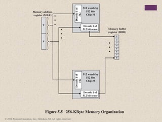
number of chips equal to the number of bits per word. As an example, Figure 5.5
shows how a memory module consisting of 256K 8-bit words could be organized. For
256K words, an 18-bit address is needed and is supplied to the module from some
external source (e.g., the address lines of a bus to which the module is attached).
The address is presented to 8 256K * 1-bit chips, each of which provides the input/
output of 1 bit.
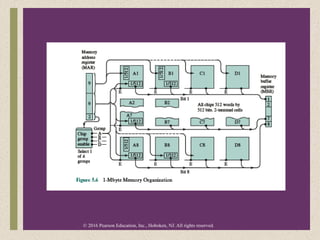
#15 This organization works as long as the size of memory equals the number of
bits per chip. In the case in which larger memory is required, an array of chips is
needed. Figure 5.6 shows the possible organization of a memory consisting of 1M
word by 8 bits per word. In this case, we have four columns of chips, each column
containing 256K words arranged as in Figure 5.5. For 1M word, 20 address lines are
needed. The 18 least significant bits are routed to all 32 modules. The high-order
2 bits are input to a group select logic module that sends a chip enable signal to one
of the four columns of modules.
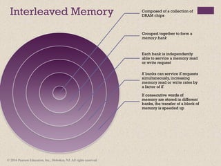
#16 Main memory is composed of a collection of DRAM memory chips. A number of
chips can be grouped together to form a memory bank. It is possible to organize
the memory banks in a way known as interleaved memory. Each bank is independently
able to service a memory read or write request, so that a system with
K banks can service K requests simultaneously, increasing memory read or write
rates by a factor of K. If consecutive words of memory are stored in different
banks, then the transfer of a block of memory is speeded up. Appendix G explores
the topic of interleaved memory.
#17 A semiconductor memory system is subject to errors. These can be categorized as
hard failures and soft errors. A hard failure is a permanent physical defect so that
the memory cell or cells affected cannot reliably store data but become stuck at
0 or 1 or switch erratically between 0 and 1. Hard errors can be caused by harsh
environmental abuse, manufacturing defects, and wear. A soft error is a random,
nondestructive event that alters the contents of one or more memory cells without
damaging the memory. Soft errors can be caused by power supply problems
or alpha particles. These particles result from radioactive decay and are distressingly
common because radioactive nuclei are found in small quantities in nearly all
materials. Both hard and soft errors are clearly undesirable, and most modern main
memory systems include logic for both detecting and correcting errors.
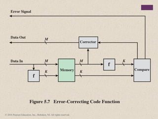
#18 Figure 5.7 illustrates in general terms how the process is carried out. When
data are to be written into memory, a calculation, depicted as a function f, is performed
on the data to produce a code. Both the code and the data are stored. Thus,
if an M-bit word of data is to be stored and the code is of length K bits, then the
actual size of the stored word is M + K bits.
When the previously stored word is read out, the code is used to detect and possibly
correct errors. A new set of K code bits is generated from the M data bits and
compared with the fetched code bits. The comparison yields one of three results:
• No errors are detected. The fetched data bits are sent out.
• An error is detected, and it is possible to correct the error. The data bits plus
error correction bits are fed into a corrector, which produces a corrected set of
M bits to be sent out.
• An error is detected, but it is not possible to correct it. This condition is reported.
Codes that operate in this fashion are referred to as error-correcting codes. A
code is characterized by the number of bit errors in a word that it can correct and detect.
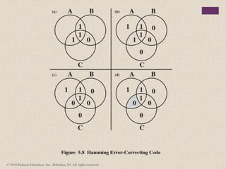
#19 The simplest of the error-correcting codes is the Hamming code devised by
Richard Hamming at Bell Laboratories. Figure 5.8 uses Venn diagrams to illustrate
the use of this code on 4-bit words (M = 4). With three intersecting circles,
there are seven compartments. We assign the 4 data bits to the inner compartments
(Figure5.8a). The remaining compartments are filled with what are called parity
bits. Each parity bit is chosen so that the total number of 1s in its circle is even
(Figure5.8b). Thus, because circle A includes three data 1s, the parity bit in that
circle is set to 1. Now, if an error changes one of the data bits (Figure 5.8c), it is easily
found. By checking the parity bits, discrepancies are found in circle A and circle
C but not in circle B. Only one of the seven compartments is in A and C but not B.
The error can therefore be corrected by changing that bit.
#20 The first three columns of Table 5.2
lists the number of check bits required for various data word lengths.
For convenience, we would like to generate a 4-bit syndrome for an 8-bit data
word with the following characteristics:
• If the syndrome contains all 0s, no error has been detected.
• If the syndrome contains one and only one bit set to 1, then an error has
occurred in one of the 4 check bits. No correction is needed.
• If the syndrome contains more than one bit set to 1, then the numerical value
of the syndrome indicates the position of the data bit in error. This data bit is
inverted for correction.
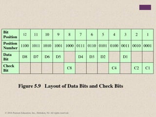
#21 To achieve these characteristics, the data and check bits are arranged into a
12-bit word as depicted in Figure 5.9. The bit positions are numbered from 1 to 12.
Those bit positions whose position numbers are powers of 2 are designated as check
bits.
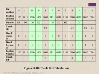
#22 Figure 5.10 illustrates the calculation. The data and check bits are
positioned properly in the 12-bit word. Four of the data bits have a value 1 (shaded
in the table), and their bit position values are XORed to produce the Hamming
code 0111, which forms the four check digits. The entire block that is stored is
001101001111. Suppose now that data bit 3, in bit position 6, sustains an error and is
changed from 0 to 1. The resulting block is 001101101111, with a Hamming code of
0111. An XOR of the Hamming code and all of the bit position values for nonzero
data bits results in 0110. The nonzero result detects an error and indicates that the
error is in bit position 6.
#23 The code just described is known as a single-error-correcting (SEC) code.
More commonly, semiconductor memory is equipped with a single-error-correcting,
double-error-detecting (SEC-DED) code. As Table 5.2 shows, such codes require
one additional bit compared with SEC codes.
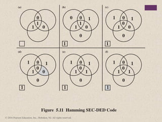
Figure 5.11 illustrates how such a code works, again with a 4-bit data word.
The sequence shows that if two errors occur (Figure 5.11c), the checking procedure
goes astray (d) and worsens the problem by creating a third error (e). To overcome
the problem, an eighth bit is added that is set so that the total number of 1s in the
diagram is even. The extra parity bit catches the error (f).
An error-correcting code enhances the reliability of the memory at the cost of
added complexity. With a 1-bit-per-chip organization, an SEC-DED code is generally
considered adequate. For example, the IBM 30xx implementations used an 8-bit SECDED
code for each 64 bits of data in main memory. Thus, the size of main memory is
actually about 12% larger than is apparent to the user. The VAX computers used a 7-bit
SEC-DED for each 32 bits of memory, for a 22% overhead. A number of contemporary
DRAMs use 9 check bits for each 128 bits of data, for a 7% overhead [SHAR03].
#24 As discussed in Chapter 1, one of the most critical system bottlenecks when using
high-performance processors is the interface to main internal memory. This interface
is the most important pathway in the entire computer system. The basic building
block of main memory remains the DRAM chip, as it has for decades; until
recently, there had been no significant changes in DRAM architecture since the
early 1970s. The traditional DRAM chip is constrained both by its internal architecture
and by its interface to the processor’s memory bus.
We have seen that one attack on the performance problem of DRAM
main memory has been to insert one or more levels of high-speed SRAM cache
between the DRAM main memory and the processor. But SRAM is much costlier
than DRAM, and expanding cache size beyond a certain point yields diminishing
returns.
In recent years, a number of enhancements to the basic DRAM architecture
have been explored. The schemes that currently dominate the market are SDRAM
and DDR-DRAM. We examine each of these in turn.
#25 One of the most widely used forms of DRAM is the synchronous DRAM
(SDRAM) [VOGL94]. Unlike the traditional DRAM, which is asynchronous, the
SDRAM exchanges data with the processor synchronized to an external clock signal
and running at the full speed of the processor/memory bus without imposing
wait states.
In a typical DRAM, the processor presents addresses and control levels to
the memory, indicating that a set of data at a particular location in memory should
be either read from or written into the DRAM. After a delay, the access time, the
DRAM either writes or reads the data. During the access-time delay, the DRAM
performs various internal functions, such as activating the high capacitance of the
row and column lines, sensing the data, and routing the data out through the output
buffers. The processor must simply wait through this delay, slowing system
performance.
With synchronous access, the DRAM moves data in and out under control of
the system clock. The processor or other master issues the instruction and address
information, which is latched by the DRAM. The DRAM then responds after a set
number of clock cycles. Meanwhile, the master can safely do other tasks while the
SDRAM is processing the request.
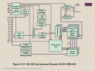
#26 Figure 5.12 shows the internal logic of a typical 256-Mb SDRAM typical
of SDRAM organization.
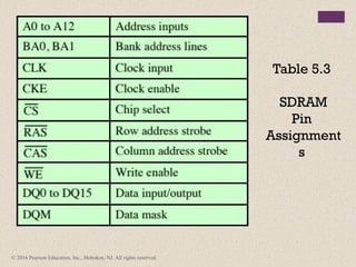
#27 Table 5.3 defines the various pin assignments.
The SDRAM employs a burst mode to eliminate the address setup time and
row and column line pre-charge time after the first access. In burst mode, a series of
data bits can be clocked out rapidly after the first bit has been accessed. This mode
is useful when all the bits to be accessed are in sequence and in the same row of the
array as the initial access. In addition, the SDRAM has a multiple-bank internal
architecture that improves opportunities for on-chip parallelism.
The mode register and associated control logic is another key feature differentiating
SDRAMs from conventional DRAMs. It provides a mechanism to
customize the SDRAM to suit specific system needs. The mode register specifies
the burst length, which is the number of separate units of data synchronously fed
onto the bus. The register also allows the programmer to adjust the latency between
receipt of a read request and the beginning of data transfer.
The SDRAM performs best when it is transferring large blocks of data serially,
such as for applications like word processing, spreadsheets, and multimedia.
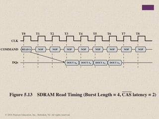
#28 Figure 5.13 shows an example of SDRAM operation.
In this case, the burst length is 4 and the latency is 2. The burst read command is
initiated by having CS and CAS low while holding RAS and WE high at the rising
edge of the clock. The address inputs determine the starting column address for the burst,
and the mode register sets the type of burst (sequential or interleave) and the burst length (1, 2,
4, 8, full page). The delay from the start of the command to when the data from the
first cell appears on the outputs is equal to the value of the CAS latency that is set
in the mode register.
#29 Although SDRAM is a significant improvement on asynchronous RAM, it still
has shortcomings that unnecessarily limit that I/O data rate that can be achieve. To
address these shortcomings a newer version of SDRAM, referred to as double-data-
rate DRAM (DDR RAM) provides several features that dramatically increase
the data rate. DDR DRAM was developed by the JEDEC Solid State Technology
Association, the Electronic Industries Alliance’s semiconductor-engineering-standardization
body. Numerous companies make DDR chips, which are widely used in
desktop computers and servers.
DDR achieves higher data rates in three ways. First, the data transfer is synchronized
to both the rising and falling edge of the clock, rather than just the rising
edge. This doubles the data rate; hence the term double data rate . Second, DDR
uses higher clock rate on the bus to increase the transfer rate. Third, a buffering
scheme is used, as explained subsequently.
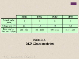
#30 JDEC has thus far defined four generations of the DDR technology (Table 5.4).
The initial DDR version makes use of a 2-bit prefetch buffer. The prefetch buffer is
a memory cache located on the SDRAM chip. It enables the SDRAM chip to preposition
bits to be placed on the data bus as rapidly as possible. The DDR I/O bus
uses the same clock rate as the memory chip, but because it can handle two bits per
cycle, it achieves a data rate that is double the clock rate. The 2-bit prefetch buffer
enables the SDRAM chip to keep up with the I/O bus.
#31 To understand the operation of the prefetch buffer, we need to look at it from
the point of view of a word transfer. The prefetch buffer size determines how many
words of data are fetched (across multiple SDRAM chips) every time a column command
is performed with DDR memories. Because the core of the DRAM is much
slower than the interface, the difference is bridged by accessing information in parallel
and then serializing it out the interface through a multiplexor (MUX). Thus,
DDR prefetches two words, which means that every time a read or a write operation
is performed, it is performed on two words of data, and bursts out of, or into, the
SDRAM over one clock cycles on both clock edges for a total of two consecutive
operations. As a result, the DDR I/O interface is twice as fast as the SDRAM core.
Although each new generation of SDRAM results is much greater capacity,
the core speed of the SDRAM has not changed significantly from generation to
generation. To achieve greater data rates than those afforded by the rather modest
increases in SDRAM clock rate, JDEC increased the buffer size. For DDR2, a 4-bit
buffer is used, allowing for words to be transferred in parallel, increasing the effective
data rate by a factor of 4. For DDR3, an 8-bit buffer is used and a factor of 8
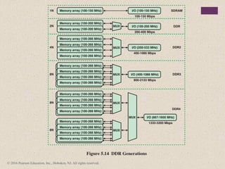
speedup is achieved (Figure 5.14).
The downside to the prefetch is that it effectively determines the minimum
burst length for the SDRAMs. For example, it is very difficult to have an efficient
burst length of four words with DDR3’s prefetch of eight. Accordingly, the JDEC
designers chose not to increase the buffer size to 16 bits for DDR4, but rather to
introduce the concept of a bank group [ALLA13]. Bank groups are separate entities
such that they allow a column cycle to complete within a bank group, but that
column cycle does not impact what is happening in another bank group. Thus,
two prefetches of eight can be operating in parallel in the two bank groups. This
arrangement keeps the prefetch buffer size the same as for DDR3, while increasing
performance as if the prefetch is larger.
Figure 5.14 shows a configuration with two bank groups. With DDR4, up to 4
bank groups can be used.
#32 Another form of semiconductor memory is flash memory. Flash memory is used
both for internal memory and external memory applications. Here, we provide a
technical overview and look at its use for internal memory.
First introduced in the mid-1980s, flash memory is intermediate between
EPROM and EEPROM in both cost and functionality. Like EEPROM, flash memory
uses an electrical erasing technology. An entire flash memory can be erased in
one or a few seconds, which is much faster than EPROM. In addition, it is possible
to erase just blocks of memory rather than an entire chip. Flash memory gets its
name because the microchip is organized so that a section of memory cells are
erased in a single action or "flash." However, flash memory does not provide bytelevel
erasure. Like EPROM, flash memory uses only one transistor per bit, and so
achieves the high density (compared with EEPROM) of EPROM.
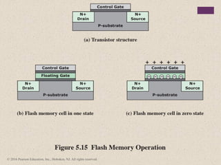
#33 Figure 5.15 illustrates the basic operation of a flash memory. For comparison, Figure
5.15a depicts the operation of a transistor. Transistors exploit the properties of
semiconductors so that a small voltage applied to the gate can be used to control the
flow of a large current between the source and the drain.
In a flash memory cell, a second gate—called a floating gate, because it is insulated
by a thin oxide layer—is added to the transistor. Initially, the floating gate
does not interfere with the operation of the transistor (Figure 5.15b). In this state,
the cell is deemed to represent binary 1. Applying a large voltage across the oxide
layer causes electrons to tunnel through it and become trapped on the floating gate,
where they remain even if the power is disconnected (Figure 5.15c). In this state, the
cell is deemed to represent binary 0. The state of the cell can be read by using external
circuitry to test whether the transistor is working or not. Applying a large voltage
in the opposite direction removes the electrons from the floating gate, returning
to a state of binary 1.
An important characteristic of flash memory is that it is persistent memory,
which means that it retains data when there is no power applied to the memory.
Thus, it is useful for secondary (external) storage, and as an alternative to random
access memory in computers.
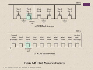
#34 There are two distinctive types of flash memory, designated as NOR and NAND
(Figure 5.16). In NOR flash memory , the basic unit of access is a bit, referred to as a
memory cell . Cells in NOR flash are connected in parallel to the bit lines so that each
cell can be read/write/erased individually. If any memory cell of the device is turned
on by the corresponding word line, the bit line goes low. This is similar in function to
a NOR logic gate.
NAND flash memory is organized in transistor arrays with 16 or 32 transistors
in series. The bit line goes low only if all the transistors in the corresponding word
lines are turned on. This is similar in function to a NAND logic gate.
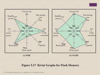
#35 Although the specific quantitative values of various characteristics of NOR
and NAND are changing year by year, the relative differences between the two
types has remained stable. These differences are usefully illustrated by the Kiviat
graphs shown in Figure 5.17.
NOR flash memory provides high-speed random access. It can read and write
data to specific locations, and can reference and retrieve a single byte. NAND reads
and writes in small blocks. NAND provides higher bit density than NOR and greater
write speed. NAND flash does not provide a random-access external address bus so
the data must be read on a blockwise basis (also known as page access), where each
block holds hundreds to thousands of bits.
For internal memory in embedded systems, NOR flash memory has traditionally
been preferred. NAND memory has made some inroads, but NOR remains the
dominant technology for internal memory. It is ideally suited for microcontrollers
where the amount of program code is relatively small and a certain amount of application
data does not vary. For example, the flash memory in Figure 1.16 is NOR
memory.
NAND memory is better suited for external memory, such as USB flash
drives, memory cards (in digital cameras, MP3 players, etc.), and in what are known
as solid-state disks (SSDs). We discuss SSDs in Chapter 6.
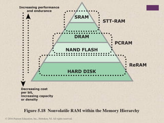
#36 The traditional memory hierarchy has consisted of three levels (Figure 5.18):
■ Static RAM (SRAM): SRAM provides rapid access time, but is the most expensive
and the least dense (bit density). SRAM is suitable for cache memory.
■ Dynamic RAM (DRAM): Cheaper, denser, and slower than SRAM, DRAM
has traditionally been the choice off-chip main memory.
■ Hard disk: A magnetic disk provides very high bit density and very low cost
per bit, with relatively slow access times. It is the traditional choice for external
storage as part of the memory hierarchy.
Into this mix, as we have seen, as been added flash memory. Flash memory has the
advantage over traditional memory that it is nonvolatile. NOR flash is best suited
to storing programs and static application data in embedded systems, while NAND
flash has characteristics intermediate between DRAM and hard disks.
Over time, each of these technologies has seen improvements in scaling: higher
bit density, higher speed, lower power consumption, and lower cost. However, for
semiconductor memory, it is becoming increasingly difficult to continue the pace of
improvement [ITRS14].
Recently, there have been breakthroughs in developing new forms of nonvolatile
semiconductor memory that continue scaling beyond flash memory. The
most promising technologies are spin-transfer torque RAM (STT-RAM), phasechange
RAM (PCRAM), and resistive RAM (ReRAM) ([ITRS14], [GOER12]).
All of these are in volume production. However, because NAND Flash and to some
extent NOR Flash are still dominating the applications, these emerging memories
have been used in specialty applications and have not yet fulfilled their original
promise to become dominating mainstream high-density nonvolatile memory. This
is likely to change in the next few years.
Figure 5.18 shows how these three technologies are likely to fit into the memory
hierarchy.
#37 STT-RAM is a new type of Magnetic RAM (MRAM), which features non-volatility,
fast writing/reading speed <10ns), and high programming endurance (>1015cycles)
and zero standby power [KULT13]. The storage capability or programmability of
MRAM arises from magnetic tunneling junction (MTJ), in which a thin tunneling
dielectric is sandwiched between two ferromagnetic layers. One ferromagnetic layer
(pinned or reference layer) is designed to have its magnetization pinned, while the
magnetization of the other layer (free layer) can be flipped by a write event. An MTJ
has a low (high) resistance if the magnetizations of the free layer and the pinned layer
are parallel (anti-parallel). In first-generation MRAM design, the magnetization of the
free layer is changed by the current-induced magnetic field. In STT-RAM, a new write
mechanism, called polarization-current-induced magnetization switching, is introduced.
For STT-RAM, the magnetization of the free layer is flipped by the electrical
current directly. Because the current required to switch an MTJ resistance state is proportional
to the MTJ cell area, STT-RAM is believed to have a better scaling property
than the first-generation MRAM. Figure 5.19a illustrates the general configuration.
STT-RAM is a good candidate for either cache or main memory.
PCRAM
Phase-change RAM is the most mature or the new technologies, with an extensive
technical literature ([RAOU09], [ZHOU09], [LEE10]).
PCRAM technology is based on a chalcogenide alloy material, which is similar
to those commonly used in optical storage media (compact discs and digital versatile
discs). The data storage capability is achieved from the resistance differences
between an amorphous (high-resistance) and a crystalline (low-resistance) phase
of the chalcogenide-based material. In SET operation, the phase change material is
crystallized by applying an electrical pulse that heats a significant portion of the cell
above its crystallization temperature. In RESET operation, a larger electrical current
is applied and then abruptly cut off in order to melt and then quench the material,
leaving it in the amorphous state. Figure 5.19b illustrates the general configuration.
PCRAM is a good candidate to replace or supplement DRAM for main
memory.
ReRAM (also known as RRAM) works by creating resistance rather than directly
storing charge. An electric current is applied to a material, changing the resistance
of that material. The resistance state can then be measured and a 1 or 0 is read as
the result. Much of the work done on ReRAM to date has focused on finding appropriate
materials and measuring the resistance state of the cells. ReRAM designs
are low voltage, endurance is far superior to flash memory, and the cells are much
smaller—at least in theory. Figure 5.19c shows one ReRam configuration.
ReRAM is a good candidate to replace or supplement both secondary storage
and main memory.