+
Core Memory
CoreMemory or Magnetic Core Memory is a RAM developed by MIT
in 1951.
It uses tiny magnetic toroids (rings), the cores, through which wires
are threaded to read or write information.
Difference between rings is roughly 1 mm.
X andY are drive lines, S is sense, Z is inhibit. Arrows indicate the
current flow direction.
Each core stores a single bit of memory.
+
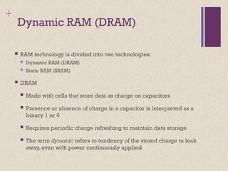
Dynamic RAM (DRAM)
RAM technology is divided into two technologies:
Dynamic RAM (DRAM)
Static RAM (SRAM)
DRAM
Made with cells that store data as charge on capacitors
Presence or absence of charge in a capacitor is interpreted as a
binary 1 or 0
Requires periodic charge refreshing to maintain data storage
The term dynamic refers to tendency of the stored charge to leak
away, even with power continuously applied
+
Static RAM
(SRAM)
Digitaldevice that uses the same
logic elements used in the
processor
Binary values are stored using
traditional flip-flop logic gate
configurations
Will hold its data as long as power
is supplied to it
+
SRAM versus DRAM
Both volatile
Power must be continuously supplied to the memory
to preserve the bit values
Dynamic cell
Simpler to build, smaller
More dense (smaller cells = more cells per unit
area)
Less expensive
Requires the supporting refresh circuitry
Tend to be favored for large memory requirements
Used for main memory
Static
Faster
Used for cache memory (both on and off chip)
SRAM
DRAM
11.
+
Read Only Memory(ROM)
Contains a permanent pattern of data that cannot be
changed or added to
No power source is required to maintain the bit values in
memory
Data or program is permanently in main memory and never
needs to be loaded from a secondary storage device
Data is actually wired into the chip as part of the fabrication
process
Disadvantages of this:
No room for error, if one bit is wrong the whole batch of ROMs
must be thrown out
Data insertion step includes a relatively large fixed cost
12.
+
Programmable ROM (PROM)
Also known as “Field Programmable ROM (FPROM)”, or One-Time
Programmable Non-volatile Memory (OTP-NVM)”
Less expensive alternative
Nonvolatile and may be written into only once
Writing process is performed electrically and may be performed by
supplier or customer at a time later than the original chip fabrication
Special equipment is required for the writing process, such as PROM
Programmer or PROM Burner
Provides flexibility and convenience
Attractive for high volume production runs
13.
Read-Mostly Memory
EPROM
Erasable programmable
read-onlymemory (Before a
write operation, all the
storage cells must be erased)
Erasure process can be
performed repeatedly
More expensive than PROM
but it has the advantage of
the multiple update
capability
EEPRO
M
Electrically erasable
programmable read-only
memory
Can be written into at any
time without erasing prior
contents, only the bytes
addressed are updated
Combines the advantage of
non-volatility with the
flexibility of being updatable
in place
More expensive than EPROM
, and also is less dense
Flash
Memory
Intermediate between
EPROM and EEPROM in
both cost and functionality.
Entire Flash can be erased in
one or few seconds.
Uses an electrical erasing
technology, does not provide
byte-level erasure
Microchip is organized so
that a section of memory
cells are erased in a single
action or “flash”. Byte-level
erasure is not possibl
14.
Interleaved Memory Composedof a collection of
DRAM chips
Grouped together to form a
memory bank
Each bank is independently
able to service a memory read
or write request
K banks can service K requests
simultaneously, increasing
memory read or write rates by
a factor of K
If consecutive words of
memory are stored in different
banks, the transfer of a block of
memory is speeded up
15.
+
Error Correction
HardFailure
Permanent physical defect
Memory cell or cells affected cannot reliably store data but become
stuck at 0 or 1 or switch erratically between 0 and 1
Can be caused by:
Harsh environmental abuse
Manufacturing defects
Wear
Soft Error
Random, non-destructive event that alters the contents of one or more
memory cells
No permanent damage to memory
Can be caused by:
Power supply problems
Alpha particles
+
Advanced DRAM Organization
One of the most critical system bottlenecks when using
high-performance processors is the interface to main
internal memory
The traditional DRAM chip is constrained both by its
internal architecture and by its interface to the
processor’s memory bus
A number of enhancements to the basic DRAM
architecture have been explored:
Table 5.3 Performance Comparison of Some DRAM Alternatives
SDRAM
RDRAM
DDR-DRAM
23.
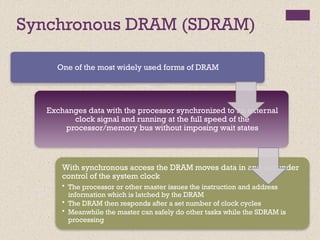
Synchronous DRAM (SDRAM)
Oneof the most widely used forms of DRAM
Exchanges data with the processor synchronized to an external
clock signal and running at the full speed of the
processor/memory bus without imposing wait states
With synchronous access the DRAM moves data in and out under
control of the system clock
• The processor or other master issues the instruction and address
information which is latched by the DRAM
• The DRAM then responds after a set number of clock cycles
• Meanwhile the master can safely do other tasks while the SDRAM is
processing
24.
RDRAM Developed byRambus
Adopted by Intel for its
Pentium and Itanium
processors
Has become the main
competitor to SDRAM
Chips are vertical packages
with all pins on one side
•Exchanges data with the processor over
28 wires no more than 12 centimeters
long
Bus can address up to 320
RDRAM chips and is rated at
1.6 GBps
Bus delivers address and
control information using an
asynchronous block-oriented
protocol
•Gets a memory request over the high-
speed bus
•Request contains the desired
address, the type of operation, and
the number of bytes in the operation
25.
+
Double Data RateSDRAM
(DDR SDRAM)
SDRAM can only send data once per bus clock cycle
Double-data-rate SDRAM can send data twice per clock
cycle, once on the rising edge of the clock pulse and once on
the falling edge
Developed by the JEDEC Solid State Technology Association
(Electronic Industries Alliance’s semiconductor-engineering-
standardization body)
26.
+
Cache DRAM (CDRAM)
Developed by Mitsubishi
Integrates a small SRAM cache onto a generic DRAM chip
SRAM on the CDRAM can be used in two ways:
It can be used as a true cache consisting of a number of 64-bit
lines
Cache mode of the CDRAM is effective for ordinary random
access to memory
Can also be used as a buffer to support the serial access of a
block of data
27.
+ Summary
Semiconductormain memory
Organization
DRAM and SRAM
Types of ROM
Chip logic
Chip packaging
Module organization
Interleaved memory
Error correction
Hard failure
Soft error
Hamming code
Advanced DRAM organization
Synchronous DRAM
Rambus DRAM
DDR SDRAM
Cache DRAM
Chapter 5
Internal
Memory
Editor's Notes
#1 Lecture slides prepared for “Computer Organization and Architecture”, 9/e, by William Stallings, Chapter 5 “Internal Memory”.
#2 We begin this chapter with a survey of semiconductor main memory subsystems,
including ROM, DRAM, and SRAM memories. Then we look at error control
techniques used to enhance memory reliability. Following this, we look at more
advanced DRAM architectures.
#3 RAM technology is divided into two technologies: dynamic and
static. A dynamic RAM (DRAM) is made with cells that store data as charge on
capacitors. The presence or absence of charge in a capacitor is interpreted as a
binary 1 or 0. Because capacitors have a natural tendency to discharge, dynamic
RAMs require periodic charge refreshing to maintain data storage. The term
dynamic refers to this tendency of the stored charge to leak away, even with power
continuously applied.
#4 In earlier computers, the most common form of random-access storage for computer
main memory employed an array of doughnut-shaped ferromagnetic loops
referred to as cores. Hence, main memory was often referred to as core, a term that
persists to this day. The advent of, and advantages of, microelectronics has long
since vanquished the magnetic core memory. Today, the use of semiconductor chips
for main memory is almost universal. Key aspects of this technology are explored
in this section.
The basic element of a semiconductor memory is the memory cell. Although a variety
of electronic technologies are used, all semiconductor memory cells share certain
properties:
• They exhibit two stable (or semistable) states, which can be used to represent
binary 1 and 0.
• They are capable of being written into (at least once), to set the state.
• They are capable of being read to sense the state.
Figure 5.1 depicts the operation of a memory cell. Most commonly, the cell
has three functional terminals capable of carrying an electrical signal. The select
terminal, as the name suggests, selects a memory cell for a read or write operation.
The control terminal indicates read or write. For writing, the other terminal
provides an electrical signal that sets the state of the cell to 1 or 0. For reading, that
terminal is used for output of the cell’s state. The details of the internal organization,
functioning, and timing of the memory cell depend on the specific integrated
circuit technology used and are beyond the scope of this book, except for a brief
summary. For our purposes, we will take it as given that individual cells can be
selected for reading and writing operations.
#5 All of the memory types that we will explore in this chapter are random access. That is,
individual words of memory are directly accessed through wired-in addressing logic.
Table 5.1 lists the major types of semiconductor memory. The most common
is referred to as random-access memory (RAM). This is, in fact, a misuse of the
term, because all of the types listed in the table are random access. One distinguishing
characteristic of memory that is designated as RAM is that it is possible
both to read data from the memory and to write new data into the memory easily
and rapidly. Both the reading and writing are accomplished through the use of
electrical signals.
The other distinguishing characteristic of RAM is that it is volatile. A RAM
must be provided with a constant power supply. If the power is interrupted, then
the data are lost. Thus, RAM can be used only as temporary storage. The two traditional
forms of RAM used in computers are DRAM and SRAM.
#6 RAM technology is divided into two technologies: dynamic and
static. A dynamic RAM (DRAM) is made with cells that store data as charge on
capacitors. The presence or absence of charge in a capacitor is interpreted as a
binary 1 or 0. Because capacitors have a natural tendency to discharge, dynamic
RAMs require periodic charge refreshing to maintain data storage. The term
dynamic refers to this tendency of the stored charge to leak away, even with power
continuously applied.
#7 Figure 5.2a is a typical DRAM structure for an individual cell that stores 1 bit.
The address line is activated when the bit value from this cell is to be read or written.
The transistor acts as a switch that is closed (allowing current to flow) if a voltage is
applied to the address line and open (no current flows) if no voltage is present on
the address line.
For the write operation, a voltage signal is applied to the bit line; a high voltage
represents 1, and a low voltage represents 0. A signal is then applied to the
address line, allowing a charge to be transferred to the capacitor.
For the read operation, when the address line is selected, the transistor turns
on and the charge stored on the capacitor is fed out onto a bit line and to a sense
amplifier. The sense amplifier compares the capacitor voltage to a reference value
and determines if the cell contains a logic 1 or a logic 0. The readout from the cell
discharges the capacitor, which must be restored to complete the operation.
Although the DRAM cell is used to store a single bit (0 or 1), it is essentially
an analog device. The capacitor can store any charge value within a range; a threshold
value determines whether the charge is interpreted as 1 or 0.
#8 In contrast, a static RAM (SRAM) is a digital device that uses the
same logic elements used in the processor. In a SRAM, binary values are stored
using traditional flip-flop logic-gate configurations (see Chapter 11 for a description
of flip-flops). A static RAM will hold its data as long as power is supplied to it.
#9 Figure 5.2b is a typical SRAM structure for an individual cell. Four transistors
(T1, T2, T3, T4) are cross connected in an arrangement that produces a stable logic
state. In logic state 1, point C1 is high and point C2 is low; in this state, T1 and T4 are off
and T2 and T3 are on. In logic state 0, point C1 is low and point C2 is high; in this state,
T1 and T4 are on and T2 and T3 are off. Both states are stable as long as the direct
current (dc) voltage is applied. Unlike the DRAM, no refresh is needed to retain data.
As in the DRAM, the SRAM address line is used to open or close a switch.
The address line controls two transistors (T5 and T6). When a signal is applied to
this line, the two transistors are switched on, allowing a read or write operation. For
a write operation, the desired bit value is applied to line B, while its complement
is applied to line B. This forces the four transistors (T1, T2, T3, T4) into the proper
state. For a read operation, the bit value is read from line B.
#10 Both static and dynamic RAMs are volatile; that is,
power must be continuously supplied to the memory to preserve the bit values.
A dynamic memory cell is simpler and smaller than a static memory cell. Thus, a
DRAM is more dense (smaller cells = more cells per unit area) and less expensive
than a corresponding SRAM. On the other hand, a DRAM requires the supporting
refresh circuitry. For larger memories, the fixed cost of the refresh circuitry is more
than compensated for by the smaller variable cost of DRAM cells. Thus, DRAMs
tend to be favored for large memory requirements. A final point is that SRAMs are
somewhat faster than DRAMs. Because of these relative characteristics, SRAM is
used for cache memory (both on and off chip), and DRAM is used for main memory.
#11 As the name suggests, a read-only memory (ROM) contains a permanent pattern
of data that cannot be changed. A ROM is nonvolatile; that is, no power source is
required to maintain the bit values in memory. While it is possible to read a ROM,
it is not possible to write new data into it. An important application of ROMs is
microprogramming, discussed in Part Four. Other potential applications include
• Library subroutines for frequently wanted functions
• System programs
• Function tables
For a modest-sized requirement, the advantage of ROM is that the data or program
is permanently in main memory and need never be loaded from a secondary storage
device.
A ROM is created like any other integrated circuit chip, with the data actually
wired into the chip as part of the fabrication process. This presents two problems:
• The data insertion step includes a relatively large fixed cost, whether one or
thousands of copies of a particular ROM are fabricated.
• There is no room for error. If one bit is wrong, the whole batch of ROMs must
be thrown out.
#12 When only a small number of ROMs with a particular memory content is
needed, a less expensive alternative is the programmable ROM (PROM). Like the
ROM, the PROM is nonvolatile and may be written into only once. For the PROM,
the writing process is performed electrically and may be performed by a supplier
or customer at a time later than the original chip fabrication. Special equipment is
required for the writing or “programming” process. PROMs provide flexibility and
convenience. The ROM remains attractive for high-volume production runs.
#13 Another variation on read-only memory is the read-mostly memory, which is
useful for applications in which read operations are far more frequent than write
operations but for which nonvolatile storage is required. There are three common
forms of read-mostly memory: EPROM, EEPROM, and flash memory.
The optically erasable programmable read-only memory (EPROM) is read
and written electrically, as with PROM. However, before a write operation, all the
storage cells must be erased to the same initial state by exposure of the packaged
chip to ultraviolet radiation. Erasure is performed by shining an intense ultraviolet
light through a window that is designed into the memory chip. This erasure process
can be performed repeatedly; each erasure can take as much as 20 minutes to
perform. Thus, the EPROM can be altered multiple times and, like the ROM and
PROM, holds its data virtually indefinitely. For comparable amounts of storage, the
EPROM is more expensive than PROM, but it has the advantage of the multiple
update capability.
A more attractive form of read-mostly memory is electrically erasable programmable
read-only memory (EEPROM). This is a read-mostly memory that can
be written into at any time without erasing prior contents; only the byte or bytes
addressed are updated. The write operation takes considerably longer than the read
operation, on the order of several hundred microseconds per byte. The EEPROM
combines the advantage of non-volatility with the flexibility of being updatable in
place, using ordinary bus control, address, and data lines. EEPROM is more expensive
than EPROM and also is less dense, supporting fewer bits per chip.
Another form of semiconductor memory is flash memory (so named because
of the speed with which it can be reprogrammed). First introduced in the mid-1980s,
flash memory is intermediate between EPROM and EEPROM in both cost and
functionality. Like EEPROM, flash memory uses an electrical erasing technology.
An entire flash memory can be erased in one or a few seconds, which is much faster
than EPROM. In addition, it is possible to erase just blocks of memory rather than
an entire chip. Flash memory gets its name because the microchip is organized so
that a section of memory cells are erased in a single action or “flash.” However,
flash memory does not provide byte-level erasure. Like EPROM, flash memory
uses only one transistor per bit, and so achieves the high density (compared with
EEPROM) of EPROM.
#14 Main memory is composed of a collection of DRAM memory chips. A number of
chips can be grouped together to form a memory bank. It is possible to organize
the memory banks in a way known as interleaved memory. Each bank is independently
able to service a memory read or write request, so that a system with
K banks can service K requests simultaneously, increasing memory read or write
rates by a factor of K. If consecutive words of memory are stored in different
banks, then the transfer of a block of memory is speeded up. Appendix E explores
the topic of interleaved memory.
#15 A semiconductor memory system is subject to errors. These can be categorized as
hard failures and soft errors. A hard failure is a permanent physical defect so that
the memory cell or cells affected cannot reliably store data but become stuck at
0 or 1 or switch erratically between 0 and 1. Hard errors can be caused by harsh
environmental abuse, manufacturing defects, and wear. A soft error is a random,
nondestructive event that alters the contents of one or more memory cells without
damaging the memory. Soft errors can be caused by power supply problems
or alpha particles. These particles result from radioactive decay and are distressingly
common because radioactive nuclei are found in small quantities in nearly all
materials. Both hard and soft errors are clearly undesirable, and most modern main
memory systems include logic for both detecting and correcting errors.
#16 Figure 5.7 illustrates in general terms how the process is carried out. When
data are to be written into memory, a calculation, depicted as a function f, is performed
on the data to produce a code. Both the code and the data are stored. Thus,
if an M-bit word of data is to be stored and the code is of length K bits, then the
actual size of the stored word is M + K bits.
When the previously stored word is read out, the code is used to detect and possibly
correct errors. A new set of K code bits is generated from the M data bits and
compared with the fetched code bits. The comparison yields one of three results:
• No errors are detected. The fetched data bits are sent out.
• An error is detected, and it is possible to correct the error. The data bits plus
error correction bits are fed into a corrector, which produces a corrected set of
M bits to be sent out.
• An error is detected, but it is not possible to correct it. This condition is reported.
Codes that operate in this fashion are referred to as error-correcting codes. A
code is characterized by the number of bit errors in a word that it can correct and detect.
#17 The simplest of the error-correcting codes is the Hamming code devised by
Richard Hamming at Bell Laboratories. Figure 5.8 uses Venn diagrams to illustrate
the use of this code on 4-bit words (M = 4). With three intersecting circles,
there are seven compartments. We assign the 4 data bits to the inner compartments
(Figure5.8a). The remaining compartments are filled with what are called parity
bits. Each parity bit is chosen so that the total number of 1s in its circle is even
(Figure5.8b). Thus, because circle A includes three data 1s, the parity bit in that
circle is set to 1. Now, if an error changes one of the data bits (Figure 5.8c), it is easily
found. By checking the parity bits, discrepancies are found in circle A and circle
C but not in circle B. Only one of the seven compartments is in A and C but not B.
The error can therefore be corrected by changing that bit.
#18 The first three columns of Table 5.2
lists the number of check bits required for various data word lengths.
For convenience, we would like to generate a 4-bit syndrome for an 8-bit data
word with the following characteristics:
• If the syndrome contains all 0s, no error has been detected.
• If the syndrome contains one and only one bit set to 1, then an error has
occurred in one of the 4 check bits. No correction is needed.
• If the syndrome contains more than one bit set to 1, then the numerical value
of the syndrome indicates the position of the data bit in error. This data bit is
inverted for correction.
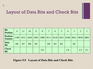
#19 To achieve these characteristics, the data and check bits are arranged into a
12-bit word as depicted in Figure 5.9. The bit positions are numbered from 1 to 12.
Those bit positions whose position numbers are powers of 2 are designated as check
bits.
#20 Figure 5.10 illustrates the calculation. The data and check bits are
positioned properly in the 12-bit word. Four of the data bits have a value 1 (shaded
in the table), and their bit position values are XORed to produce the Hamming
code 0111, which forms the four check digits. The entire block that is stored is
001101001111. Suppose now that data bit 3, in bit position 6, sustains an error and is
changed from 0 to 1. The resulting block is 001101101111, with a Hamming code of
0111. An XOR of the Hamming code and all of the bit position values for nonzero
data bits results in 0110. The nonzero result detects an error and indicates that the
error is in bit position 6.
#21 The code just described is known as a single-error-correcting (SEC) code.
More commonly, semiconductor memory is equipped with a single-error-correcting,
double-error-detecting (SEC-DED) code. As Table 5.2 shows, such codes require
one additional bit compared with SEC codes.
Figure 5.11 illustrates how such a code works, again with a 4-bit data word.
The sequence shows that if two errors occur (Figure 5.11c), the checking procedure
goes astray (d) and worsens the problem by creating a third error (e). To overcome
the problem, an eighth bit is added that is set so that the total number of 1s in the
diagram is even. The extra parity bit catches the error (f).
An error-correcting code enhances the reliability of the memory at the cost of
added complexity. With a 1-bit-per-chip organization, an SEC-DED code is generally
considered adequate. For example, the IBM 30xx implementations used an 8-bit SECDED
code for each 64 bits of data in main memory. Thus, the size of main memory is
actually about 12% larger than is apparent to the user. The VAX computers used a 7-bit
SEC-DED for each 32 bits of memory, for a 22% overhead. A number of contemporary
DRAMs use 9 check bits for each 128 bits of data, for a 7% overhead [SHAR97].
#22 As discussed in Chapter 2, one of the most critical system bottlenecks when using
high-performance processors is the interface to main internal memory. This interface
is the most important pathway in the entire computer system. The basic building
block of main memory remains the DRAM chip, as it has for decades; until
recently, there had been no significant changes in DRAM architecture since the
early 1970s. The traditional DRAM chip is constrained both by its internal architecture
and by its interface to the processor’s memory bus.
We have seen that one attack on the performance problem of DRAM
main memory has been to insert one or more levels of high-speed SRAM cache
between the DRAM main memory and the processor. But SRAM is much costlier
than DRAM, and expanding cache size beyond a certain point yields diminishing
returns.
In recent years, a number of enhancements to the basic DRAM architecture
have been explored, and some of these are now on the market. The schemes that currently
dominate the market are SDRAM, DDR-DRAM, and RDRAM. Table 5.3
provides a performance comparison. CDRAM has also received considerable attention.
We examine each of these approaches in this section.
#23 One of the most widely used forms of DRAM is the synchronous DRAM
(SDRAM) [VOGL94]. Unlike the traditional DRAM, which is asynchronous, the
SDRAM exchanges data with the processor synchronized to an external clock signal
and running at the full speed of the processor/memory bus without imposing
wait states.
In a typical DRAM, the processor presents addresses and control levels to
the memory, indicating that a set of data at a particular location in memory should
be either read from or written into the DRAM. After a delay, the access time, the
DRAM either writes or reads the data. During the access-time delay, the DRAM
performs various internal functions, such as activating the high capacitance of the
row and column lines, sensing the data, and routing the data out through the output
buffers. The processor must simply wait through this delay, slowing system
performance.
With synchronous access, the DRAM moves data in and out under control of
the system clock. The processor or other master issues the instruction and address
information, which is latched by the DRAM. The DRAM then responds after a set
number of clock cycles. Meanwhile, the master can safely do other tasks while the
SDRAM is processing the request.
#24 RDRAM, developed by Rambus [FARM92, CRIS97], has been adopted by Intel
for its Pentium and Itanium processors. It has become the main competitor to
SDRAM. RDRAM chips are vertical packages, with all pins on one side. The chip
exchanges data with the processor over 28 wires no more than 12 centimeters long.
The bus can address up to 320 RDRAM chips and is rated at 1.6 GBps.
The special RDRAM bus delivers address and control information using
an asynchronous block-oriented protocol. After an initial 480 ns access time,
this produces the 1.6 GBps data rate. What makes this speed possible is the bus
itself, which defines impedances, clocking, and signals very precisely. Rather than
being controlled by the explicit RAS, CAS, R/W, and CE signals used in conventional
DRAMs, an RDRAM gets a memory request over the high-speed bus. This
request contains the desired address, the type of operation, and the number of
bytes in the operation.
#25 SDRAM is limited by the fact that it can only send data to the processor once per
bus clock cycle. A new version of SDRAM, referred to as double-data-rate SDRAM
can send data twice per clock cycle, once on the rising edge of the clock pulse and
once on the falling edge.
DDR DRAM was developed by the JEDEC Solid State Technology
Association, the Electronic Industries Alliance’s semiconductor-engineering-standardization
body. Numerous companies make DDR chips, which are widely used in
desktop computers and servers.
#26 Cache DRAM (CDRAM), developed by Mitsubishi [HIDA90, ZHAN01], integrates
a small SRAM cache (16 Kb) onto a generic DRAM chip.
The SRAM on the CDRAM can be used in two ways. First, it can be used as a
true cache, consisting of a number of 64-bit lines. The cache mode of the CDRAM
is effective for ordinary random access to memory.
The SRAM on the CDRAM can also be used as a buffer to support the serial
access of a block of data. For example, to refresh a bit-mapped screen, the CDRAM
can prefetch the data from the DRAM into the SRAM buffer. Subsequent accesses
to the chip result in accesses solely to the SRAM.