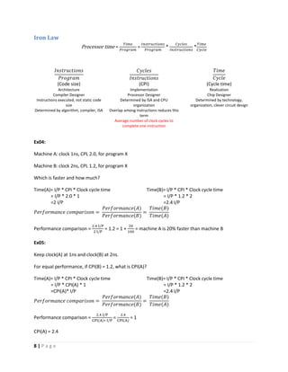
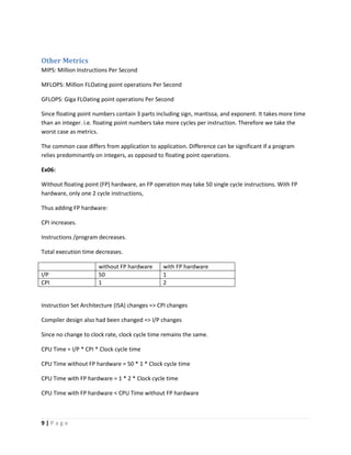
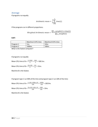
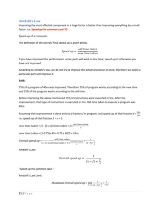
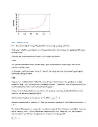
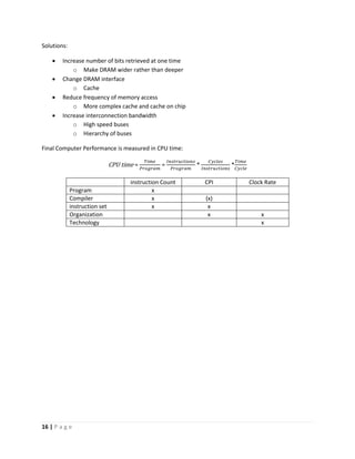
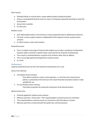
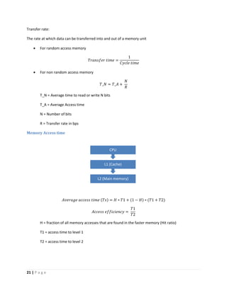
1 | P a g e
Computer Architecture
IN 2320
Lesson 02 – Introduction
Computer architecture:
 Deals with the functional behavior of a computer system as viewed by a programmer
Ex: the size of a data type –32 bits to an integer
Computer organization:
 Deals with structural relationships that are not visible to the programmer
Ex: clock frequency or the size of the physical memory
Levels of a computer:
1. User Level: Application Programs (HIGH LEVEL)
2. High level languages
3. Assembly Language/ Machine Code
4. Microprogrammed/ Hardwired Control
5. Functional Units (Memory, ALU, etc)
6. Logic Gates
7. Transistors and Wires (LOW LEVEL)
Computer Architecture-Definition:
 The attributes of the computer system that are visible to programmers i.e. the attributes of the
computer system that have a direct impact on the logical execution of a program
Ex: the instruction set, the size of a data type, techniques of addressing the memory
EX: Architectural issue is whether a computer will have a multiply instruction
Computer Organization-Definition:
 The operational units and their interconnection that realize the architectural specifications
Ex: control signals, interface between computer and peripherals, memory technology used
Ex: Organizational issue is whether multiply instruction is implemented using the a separate cct
or whether it is implemented using the repeated use of adder cct.
Organozational decision may based on the several parameters such as anticipated frequency of
the use of multiply instruction.
2 | P a g e
Forces on Computer Architecture:
 Technology
 Programming Languages
 Applications
 OS
 History
The Computer Architect’s view:
 Architect is concerned with design & performance
 Designs the ISA for optimum programming utility and optimum performance of implementation
 Designs the hardware for best implementation of the instructions
 Uses performance measurement tools, such as benchmark programs, to see that goals are met
 Balances performance of building blocks such as CPU, memory, I/O devices, and
interconnections
 Meets performance goals at lowest cost
Factors involving when selecting a better computer are;
1. COST factors
a. Cost of hardware design
b. Cost of software design (OS, applications)
c. Cost of manufacture
d. Cost of end purchaser
2. PERFORMANCE factors
a. What programs will be run?
b. How frequently will they be run?
c. How big are the programs?
d. How many users?
e. How sophisticated are the users (User level)?
f. What I/O devices are necessary?
g. There are two ways to make computers go faster.
i. Wait sometime (year). Implement in a faster/better/newer technology.
1. More transistors will fit on a single chip.
2. More pins can be placed around the IC.
3. The process used will have electronic devices (transistors) that switch
faster.
ii. New/innovative architectures and architectural features, and clever
implementations of existing architectures.
3 | P a g e
Higher Computer performance may involve one or more of the following:
 Short response time for a given piece or work
o The total time taken by a functional unit to respond to a request for service
o Functional unit/ execution unit is a part of CPU that performs the operations and
calculations as instructed by a computer.
 High throughput (rate or processing work)
o Rate at which something can be processed
 Low utilization of computing resources
o System resources(practical): physical or virtual entities of limited availability
 Ex: memory, processing capacity, network speed
o Computational resources(abstract): resources used for solving a computational problem
 Ex: computational time, memory space
 Fast data compression and decompression
 High bandwidth
 Short data transmission time
*note red coloured performance factors are the area of interest.
Throughput:
if(no overlap or if no parallelism)
throughput = 1/average response time
else
throughput > 1/average response time
//the number of parallel processing computers are also important
Elapsed time/response time:
 Elapsed time = Response time = CPU time + I/O wait time
 CPU time = time spent running a program
 Performance= 1/response time
Since we are more concerned about CPU time,
Performance = 1/CPU time
*note Improve Performance
1. Faster the CPU
Helps to improve both response time and throughput
2. Add more CPUs
Helps to improve throughput and perhaps response time due to less queuing
4 | P a g e
*Note: Selection is depend on what is important to whom, i.e. cost factors and performance factors
Ex 01: Computer system user
 Goal: Minimize elapsed time for program=time_end-time_start
Called response time (counted in ms)
Ex 02: Computer Center Manager
 Goal: Maximize completion rate = no. of jobs per second
Called throughput (counted per sec)
Factors driving architecture:
 Effective use of new technology
 Can a desired performance improvement
Performance Metrics
Values derived from some fundamental measurements:
 Count of how many times an event occurs
 Duration of a time interval
 Size of some parameter
Some basic metrics include:
 Response time
o Elapse time from request to response
o Elapsed time = Response time = CPU time + I/O wait time
CPU time = time spent running a program
Performance time= 1/response time
Since we are more concerned about CPU time,
Performance time= 1/CPU time
o CPU time is affected by;
 Number of instructions in the program
 Average number of clock cycles to complete one instruction
 Clock cycle time
 Throughput
o Jobs or operations completed per unit of time
 Bandwidth
o Bits per second
 Resource utilization
5 | P a g e
Standard benchmark metrics
 SPEC
 TCP
Characteristics of good metrics:
 Linear
o Proportional to the actual system performance
 Reliable
o Larger value -> better performance
 Repeatable
o Deterministic when measured
 Consistent
o Units and definition constant across systems
 Independent
o Independent from influence of vendors
 Easy to measure
Some examples of Standard Metrics:
 MIPS
 MFLOPS, GFLOPS, TFLOPS, PFLOPS
 SPEC metrics
 TCP metrics
Parameters of Performance Metrics:
 Clock rate (=1/Clock cycle time)
 Instructions per program (I/P)
 Average clock cycles per instruction (CPI)
 Service time
 Interarrival time (time between arrivals of successive requests)
 Number of users
 Think time
*note Execution time (CPU time, runtime) = I/P * CPI * clock cycle time <= Iron Law
All the three factors are combined to affect the metric Execution time.
 I/P -> depend on compiler
 CPI -> depend on CPU design/organization
 Clock cycle time -> processor architecture
6 | P a g e
Ex01:
Our program takes 10s to run on computer A, which has 400 MHz clock. We want it to run in 6s. The
designer says that the clock rate can be increased, but it will cause the total number of clock cycles for
the program to increase to 1.2 times the previous value. What is the minimum clock rate required to get
the desired speedup?
Answer:
Old Machine A New Machine A
Runtime 10s 6s
Clock Rate 400Hz CR
Let Total number of clock cycles per program in old machine A = x
Since clock cycles per program = Clock Rate * Runtime
x = 400 * 10 = 4000 cycles
Total number of clock cycles per program in new machine A = 1.2 x
= 1.2 * 4000
= 6 * CR
6 * CR = 1.2 * 4000
CR = 800Hz
Workload:
 A test case for the system
Benchmark:
 A set of workload which together is representative of ‘my program’ should be reproducible.
Ex02:
Which is faster? A or B?
Test Case Machine A Machine B
1 1s 10s
2 100s 10s
Assume Test Case 1 type processes happen 99% of the time
7 | P a g e
Answer:
We have to obtain the weighted average of runtime.
Weighted average for A =
1(99)+ 100(1)
100
= 1.99 s <= answer is A
Weighted average for B =
10(99)+ 10(1)
100
= 10 s
*note
Cost of improving the processor is high. But if you find that you are needed a particular circuit 99% of
the time (ex: multiplication instruction), then you can improve that circuit from 2, 3 factors. You will
improve the performance as a whole that way.
Performance comparison
Performance =
1
𝑡𝑖𝑚𝑒
There are 2 machines A and B.
Performance(A) =
1
𝑡𝑖𝑚𝑒(𝐴)
Performance(B) =
1
𝑡𝑖𝑚𝑒(𝐵)
Therefore;
Performance(A)
Performance(B)
=
𝑡𝑖𝑚𝑒(𝐵)
𝑡𝑖𝑚𝑒(𝐴)
= 1 +
𝑥
100
iff A is x% faster than B
Ex03:
time(B) = 10s, time(B) = 15s
Performance(A)
Performance(B)
=
𝑡𝑖𝑚𝑒(𝐵)
𝑡𝑖𝑚𝑒(𝐴)
=
15
10
= 1.5 = 1 +
50
100
i.e. A is 50% faster than B
Breaking down performance:
 A program is broken into instructions.
o Hardware is aware of instructions, not programs.
 At lower level, hardware breaks into instructions into cycles.
o Lowe level state machines change state every cycle
 For example 500MHz P-III runs 500M cycles/sec, 1 cycle = 2ns
8 | P a g e
Iron Law
Processor time =
𝑇𝑖𝑚𝑒
𝑃𝑟𝑜𝑔𝑟𝑎𝑚
=
𝐼𝑛𝑠𝑡𝑟𝑢𝑐𝑡𝑖𝑜𝑛𝑠
𝑃𝑟𝑜𝑔𝑟𝑎𝑚
*
𝐶𝑦𝑐𝑙𝑒𝑠
𝐼𝑛𝑠𝑡𝑟𝑢𝑐𝑡𝑖𝑜𝑛𝑠
*
𝑇𝑖𝑚𝑒
𝐶𝑦𝑐𝑙𝑒
𝐼𝑛𝑠𝑡𝑟𝑢𝑐𝑡𝑖𝑜𝑛𝑠
𝑃𝑟𝑜𝑔𝑟𝑎𝑚
𝐶𝑦𝑐𝑙𝑒𝑠
𝐼𝑛𝑠𝑡𝑟𝑢𝑐𝑡𝑖𝑜𝑛𝑠
𝑇𝑖𝑚𝑒
𝐶𝑦𝑐𝑙𝑒
(Code size) (CPI) (Cycle time)
Architecture Implementation Realization
Compiler Designer Processor Designer Chip Designer
Instructions executed, not static code
size
Determined by algorithm, compiler, ISA
Determined by ISA and CPU
organization
Overlap among instructions reduces this
term
Average number of clock cycles to
complete one instruction
Determined by technology,
organization, clever circuit design
Ex04:
Machine A: clock 1ns, CPL 2.0, for program X
Machine B: clock 2ns, CPL 1.2, for program X
Which is faster and how much?
Time(A)= I/P * CPI * Clock cycle time
= I/P * 2.0 * 1
=2 I/P
Time(B)= I/P * CPI * Clock cycle time
= I/P * 1.2 * 2
=2.4 I/P
𝑃𝑒𝑟𝑓𝑜𝑟𝑚𝑎𝑛𝑐𝑒 𝑐𝑜𝑚𝑝𝑎𝑟𝑖𝑠𝑜𝑛 =
𝑃𝑒𝑟𝑓𝑜𝑟𝑚𝑎𝑛𝑐𝑒(𝐴)
𝑃𝑒𝑟𝑓𝑜𝑟𝑚𝑎𝑛𝑐𝑒(𝐵)
=
𝑇𝑖𝑚𝑒(𝐵)
𝑇𝑖𝑚𝑒(𝐴)
Performance comparison =
2.4 I/P
2 I/P
= 1.2 = 1 +
20
100
= machine A is 20% faster than machine B
Ex05:
Keep clock(A) at 1ns and clock(B) at 2ns.
For equal performance, if CPI(B) = 1.2, what is CPI(A)?
Time(A)= I/P * CPI * Clock cycle time
= I/P * CPI(A) * 1
=CPI(A)* I/P
Time(B)= I/P * CPI * Clock cycle time
= I/P * 1.2 * 2
=2.4 I/P
𝑃𝑒𝑟𝑓𝑜𝑟𝑚𝑎𝑛𝑐𝑒 𝑐𝑜𝑚𝑝𝑎𝑟𝑖𝑠𝑜𝑛 =
𝑃𝑒𝑟𝑓𝑜𝑟𝑚𝑎𝑛𝑐𝑒(𝐴)
𝑃𝑒𝑟𝑓𝑜𝑟𝑚𝑎𝑛𝑐𝑒(𝐵)
=
𝑇𝑖𝑚𝑒(𝐵)
𝑇𝑖𝑚𝑒(𝐴)
Performance comparison =
2.4 I/P
CPI(A)∗ I/P
=
2.4
CPI(A)
= 1
CPI(A) = 2.4
9 | P a g e
Other Metrics
MIPS: Million Instructions Per Second
MFLOPS: Million FLOating point operations Per Second
GFLOPS: Giga FLOating point operations Per Second
Since floating point numbers contain 3 parts including sign, mantissa, and exponent. It takes more time
than an integer. i.e. floating point numbers take more cycles per instruction. Therefore we take the
worst case as metrics.
The common case differs from application to application. Difference can be significant if a program
relies predominantly on integers, as opposed to floating point operations.
Ex06:
Without floating point (FP) hardware, an FP operation may take 50 single cycle instructions. With FP
hardware, only one 2 cycle instructions,
Thus adding FP hardware:
CPI increases.
Instructions /program decreases.
Total execution time decreases.
without FP hardware with FP hardware
I/P 50 1
CPI 1 2
Instruction Set Architecture (ISA) changes => CPI changes
Compiler design also had been changed => I/P changes
Since no change to clock rate, clock cycle time remains the same.
CPU Time = I/P * CPI * Clock cycle time
CPU Time without FP hardware = 50 * 1 * Clock cycle time
CPU Time with FP hardware = 1 * 2 * Clock cycle time
CPU Time with FP hardware < CPU Time without FP hardware
10 | P a g e
Average
If programs run equally:
𝐴𝑟𝑖𝑡ℎ𝑚𝑒𝑡𝑖𝑐 𝑚𝑒𝑎𝑛 =
1
𝑛
∑ 𝑡𝑖𝑚𝑒(𝑡)
𝑛
𝑡=1
If the programs run in different proportions:
𝑊𝑒𝑖𝑔ℎ𝑡𝑒𝑑 𝐴𝑟𝑖𝑡ℎ𝑚𝑒𝑡𝑖𝑐 𝑚𝑒𝑎𝑛 =
∑ 𝑤𝑒𝑖𝑔ℎ𝑡(𝑡) x 𝑡𝑖𝑚𝑒(𝑡)𝑛
𝑡=1
∑ 𝑤𝑒𝑖𝑔ℎ𝑡(𝑡)𝑛
𝑡=1
Ex07:
Machine A CPU time Machine B CPU time
Program 1 1ns 10ns
Program 2 1000ns 100ns
What is the fastest computer?
If programs run equally:
Mean CPU time of A =
1+1000
2
=
1001
2
= 500.5ns
Mean CPU time of B =
10+100
2
=
110
2
= 55ns
Machine B is the fastest.
If program type 1 run 90% of the time and program type 2 run 10% of the time:
Mean CPU time of A =
1 x 90 +1000 x 10
100
=
10090
100
= 100.9ns
Mean CPU time of B =
10 x 90 +100 x 10
100
=
1900
100
= 19ns
Machine B is the fastest.
11 | P a g e
Amdahl’s Law
Improving the most affected component in a large factor is better than improving everything by a small
factor. i.e. Speedup the common case! 
Speed-up of a computer:
The definition of the overall/ final speed-up is given below.
𝑆𝑝𝑒𝑒𝑑 𝑢𝑝 =
𝑜𝑙𝑑 𝑡𝑖𝑚𝑒 𝑡𝑎𝑘𝑒𝑛
𝑛𝑒𝑤 𝑡𝑖𝑚𝑒 𝑡𝑎𝑘𝑒𝑛
If you have improved the performance, some parts will work in less time; speed-up>1 otherwise you
have not improved.
According to Amdahl’s law, we do not try to improve the whole processor at once; therefore we select a
particular part and improve it.
Ex08:
75% of a program of 40ns was improved. Therefore 75% of program works according to the new time
and 25% of the program works according to the old time.
Before improving the above mentioned 75% of instructions were executed in 5ns. After the
improvement, that type of instructions is executed in 1ns. Old time taken to execute a program was
40ns
Assuming that improvement is done only to a fraction f in program, and speed-up of that fraction f =
5𝑛𝑠
1𝑛𝑠
i.e. speed-up of that fraction f = s = 5
new time taken = (1 - f) x old time taken + f x
𝑜𝑙𝑑 𝑡𝑖𝑚𝑒 𝑡𝑎𝑘𝑒𝑛
𝑠
new time taken = (1-0.75)x 40 + 0.75 x 40/5 = 16ns
Overall speed up =
𝑜𝑙𝑑 𝑡𝑖𝑚𝑒 𝑡𝑎𝑘𝑒𝑛
(1−𝑓) x 𝑜𝑙𝑑 𝑡𝑖𝑚𝑒 𝑡𝑎𝑘𝑒𝑛 + 𝑓 x
𝑜𝑙𝑑 𝑡𝑖𝑚𝑒 𝑡𝑎𝑘𝑒𝑛
𝑠
=
1
(1−𝑓)+
𝑓
𝑠
Amdahl’s Law:
𝑂𝑣𝑒𝑟𝑎𝑙𝑙 𝑠𝑝𝑒𝑒𝑑 𝑢𝑝 =
1
(1 − 𝑓) +
𝑓
𝑠
“Speed up the common case.”
Amdahl’s Law Limit:
Maximum Overall speed up = lim
𝑠→∞
1
(1−𝑓)+
𝑓
𝑠
=
1
1−𝑓
12 | P a g e
Figure 1: Amdahl's Law limit
If (1 – f) is nontrivial (extremely difficult and time consuming) speed up is limited.
If a program is highly sequential, there is no any solution other than increase the speedup of a fraction
of the program.
If parallel, we have the additional option to increase the parallelism.
*note
The performance enhancement possible with a given improvement is limited by the amount the
improved feature is used.
Ex: To make a significant impact on the CPI, identify the instructions that occur more frequently and
optimize the design for them.
Ex09:
Program runs In 100s multiplies 80% of the time. Designer M can improve the speed-up of multiply
operations. Now I am a user and I need to make My program 5 times faster. How much speed-up should
M achieve to allow me to reach my overall speed-up goal?
First we need to check whether we can achieve this speed up practically. So let us find the maximum
speed up that we can achieve by f of 80%.
Maximum speed up that we can achieve by f of 80% =
1
1−0.8
=
1
0.2
= 5
We can achieve an overall speed up of 5 if we give an infinite speed up for multiplication instruction. i.e.
s → ∞
The designer M was asked to improve the overall speed up to 5. Theoretically we proved that maximum
overall speed up is also 5. Normally practical maximum speed up is always less than the theoretical
maximum speed up. Therefore this goal cannot be achieved by designer M.
13 | P a g e
Ex10:
Usage frequency and the cycles per operations were given below.
Operation Frequency Cycles per operation
ALU 42% 1
Load 21% 1
Store 12% 2
Branch 24% 2
Assume stores can execute in 1 cycle by slowing clock by 15%. Is it worth implementing this?
Execution time (CPU time, runtime) = I/P * CPI * clock cycle time
CPI = Average number of instructions per cycle
Old CPI =
42 x 1+21 x 1+12 x 2+24 x 2
100
= 1.36
New CPI =
42 x 1+21 x 1+12 x 1+24 x 2
100
= 1.24
Let Old clock cycle time = x
Since clock will be slowed down by 15%, the clock cycle time will be increase by 15% due to inverse
relationship. (clock rate = 1 / clock cycle time)
Therefore New clock cycle time = 1.15x
Since the architecture of the compiler remains constant, the I/P is constant.
Old machine New machine
I/P I/P I/P
CPI 1.36 1.24
Clock cycle time x 1.15x
Old CPU time = I/P x 1.36 x x
New CPU time = I/P x 1.24 x 1.15x
Speed up =
I/P x 1.36 x 𝑥
I/P x 1.24 x 1.15𝑥
=
1.36
1.24 x 1.15
= 0.95
The speed up < 1
Old CPU time
New CPU time
< 1
Old CPU time < New CPU time
This implementation is not worth doing. 
14 | P a g e
Generations of Computer
 Vacuum tube
 Transistor
 Small scale IC
 Medium scale IC
 Large scale IC
 Very large scale IC
 Ultra large scale IC
 AI
Moore’s Law
The observation that, over the history of computing hardware, the number of transistors in a dense IC
has doubled approximately every two years
Figure 2: CPU Transistor Counts 1971 - 2008 and Moore's Law
Consequences:
 Higher packing density means shorter electrical paths, giving higher performance in speed
 Smaller size gives increased flexibility
 Reduced power and cooling requirements
 Fewer interconnections increases reliability
Cost of a chip has remained almost unchanged.
15 | P a g e
Requirements changed over time:
 Image processing
 Speech recognition
 Video conferencing
 Multimedia authoring
 Voice and video annotation files
 Simulation modeling
Ways to speeding up the processor:
 Pipelining
 On board cache
 On board L1 and L2 cache
 Brand prediction
 Data flow analysis
 Speculative execution
Performance mismatch:
 Processor speed increases
 Memory capacity increases
 But memory speed always lags behind processor speed
Figure 3: DRAM (Main Memory) and Processor characteristics
16 | P a g e
Solutions:
 Increase number of bits retrieved at one time
o Make DRAM wider rather than deeper
 Change DRAM interface
o Cache
 Reduce frequency of memory access
o More complex cache and cache on chip
 Increase interconnection bandwidth
o High speed buses
o Hierarchy of buses
Final Computer Performance is measured in CPU time:
CPU time =
𝑇𝑖𝑚𝑒
𝑃𝑟𝑜𝑔𝑟𝑎𝑚
=
𝐼𝑛𝑠𝑡𝑟𝑢𝑐𝑡𝑖𝑜𝑛𝑠
𝑃𝑟𝑜𝑔𝑟𝑎𝑚
*
𝐶𝑦𝑐𝑙𝑒𝑠
𝐼𝑛𝑠𝑡𝑟𝑢𝑐𝑡𝑖𝑜𝑛𝑠
*
𝑇𝑖𝑚𝑒
𝐶𝑦𝑐𝑙𝑒
instruction Count CPI Clock Rate
Program x
Compiler x (x)
instruction set x x
Organization x x
Technology x
17 | P a g e
Lesson 03 – Computer Memory
A memory unit is a collection of storage cells together with necessary circuits for information transfer in
and out of storage.
Memory stores binary information in groups of bits called words.
A word in a memory is a fundamental unit of information in a memory.
 Hold series of 1’s and 0’s
 Represent numbers, instruction codes, characters etc.
A group of 8 bits called as a byte which is fundamental unit of metric.
Usually a word is a multiple of bytes.
Classification of memory due to key Characteristics:
 Location
o CPU (registers)
o Internal (Main Memory/ RAM)
o External (backing storage)
 Capacity
o Word size (The natural unit of organization)
o Number of words (Or bytes)
 Unit of transfer
o Internal (depend on the bus width)
o External (memory block)
o Addressable unit (smallest unit which can be uniquely addressed, word internally)
 Access method
o Sequential (ex: tape)
o Direct (ex: disk)
o Random (ex: RAM)
o Associative (ex: cache, within words)
 Performance
o Access time (latency)
o Memory cycle time
o Transfer rate
 Physical type
o Semiconductor (ex: SRAM, caches)
o Magnetic (ex: disk and tape)
o Optical (CD and DVD)
o Others (ex: bubble)
18 | P a g e
 Physical characteristics
o Decay (leak charges in capacitors in DRAM)
o Volatility
o Erasable
o Power consumption
 Organization
Figure 4: Memory Hierarchy
Classification of memory due to key Characteristics:
Location
Whether memory is internal or external to the computer
Internal memory:
 Often refers to the Main Memory
 But there are other types of internal memory too which are associate with the processor
o Register memory
o Cache memory
External memory:
 Refers to peripheral storage devices, such as disk and tape
 Accessible to the processor via I/O controllers
19 | P a g e
Capacity
Internal memory:
 Measured in terms of bytes or words
 Order of 1, 2, 4, 8 bytes
External memory:
 Measured in terms of hundreds of Mega bytes or Giga bytes
Unit of transfer
Internal memory:
 Refers to the number of data lines into and out of the memory module
 This may equal to the word length, but is often larger 128, 256 bits
Concepts related to internal memory:
 Word
o Natural unit of organization of memory
o The size of the word is typically equal to the number of bits used to represent a number
and to the instruction length. But there are exceptional cases too.
 Addressable units
o Refers to the location which can be uniquely addressed
o In some systems addressable unit is the word.
o Many systems allow addressing at byte level.
o In any case relationship between the length in bits A of an address and the number N of
addressable units is 2A
= N, range of addressable units 0 to (2A
– 1)
External memory:
 Data are often transferred in much larger units than a word, and these are referred to as blocks.
Access method
Methods of accessing units of data
Sequential access:
 Memory is organized into units of data called records.
 Access must be made in specific linear sequence.
 Each intermediate record from current location to the desired location should be passed and
rejected.
 Time to access arbitrary record is highly variable depending on the location of the data and
previous location of the reading header.
 Ex: tape
20 | P a g e
Direct access:
 Individual blocks or records have a unique address based on physical location.
 Access is accomplished by direct access to reach a vicinity plus sequential searching to reach the
final location.
 Access time is variable.
 Ex: Disk units
Random access:
 Each addressable location in the memory is unique, physically wired in addressing mechanism.
 The time to access a given location is independent of the sequence of prior accesses and is
constant.
 Ex: Main memory, some cache systems
Associative access:
 This is a random access type of memory that enables one to make a comparison of desired bit
locations within a word for a specific match, and to do this for all words simultaneously.
 Thus a word is retrieved based on a portion of its contents rather than its address.
 This is a very high speed searching kind of a memory access.
 Ex: cache
Performance
Capacity and performance are the most important characteristics for a user
Access time (latency):
 For Random Access memory
Time takes to perform a read or write operation, i.e. time from the instant that an
address is presented to the memory to the instant that data have been stored or made
available for use
 For non Random Access memory
Time takes to position the read-write mechanism at the desired location
Memory Cycle time:
 Primarily applied for random access memory
 Memory cycle time = Access time + Time required before a second success can commence
 Time required before a second success can commence is the time taken to recover.
 Memory cycle time is concerned with the system bus, not the processor.
21 | P a g e
Transfer rate:
The rate at which data can be transferred into and out of a memory unit
 For random access memory
𝑇𝑟𝑎𝑛𝑠𝑓𝑒𝑟 𝑡𝑖𝑚𝑒 =
1
𝐶𝑦𝑐𝑙𝑒 𝑡𝑖𝑚𝑒
 For non random access memory
𝑇_𝑁 = 𝑇_𝐴 +
𝑁
𝑅
T_N = Average time to read or write N bits
T_A = Average Access time
N = Number of bits
R = Transfer rate in bps
Memory Access time
𝐴𝑣𝑒𝑟𝑎𝑔𝑒 𝑎𝑐𝑐𝑒𝑠𝑠 𝑡𝑖𝑚𝑒 (𝑇𝑠) = 𝐻 ∗ 𝑇1 + (1 − 𝐻) ∗ (𝑇1 + 𝑇2)
𝐴𝑐𝑐𝑒𝑠𝑠 𝑒𝑓𝑓𝑖𝑐𝑖𝑒𝑛𝑐𝑦 =
𝑇1
𝑇2
H = fraction of all memory accesses that are found in the faster memory (Hit ratio)
T1 = access time to level 1
T2 = access time to level 2
L2 (Main memory)
L1 (Cache)
CPU
22 | P a g e
Ex01:
Suppose a processor has two levels of memory. Level 1 contains 1000 words and has access time of
0.01μs. Level 2 contains 100000 words and has access time of 0.1 μs. Level 1 can directly access. If it in
level 2, then word first transferred into level 1 and then access by the processor.
For simplicity we ignore the time taken to processor to determine whether the word is in level 1 or 2.
For high percentage of level 1 access, the average access time is much closer to that of level 1 than level
2.
Suppose we have 95% of the memory access found in Level 1
Ts = 0.95 * 0.01 µs + (1 - 0.95) * (0.01 µs + 0.1 µs)
Ts= 0.015 µs
Locality of reference
Also known as the principle of locality, the phenomenon in which the same values or related storage
locations are frequently accessed.
Two basic types of reference locality
1. Temporal coherence
 There is a higher probability of repeated access to any data item that has been accessed
in the recent past.
 Ex: for loop
2. Spatial coherence
 There is a higher probability of access to any data item that is physically closer to any
other data item that has been access in the recent past.
 Ex: arrays
Physical Characteristics
Figure 5: Memory Hierarchy list and how physical characteristics differ accordingly.
23 | P a g e
Semiconductor Memory
Basic element is the cell.
Cell is able to be in one of the two states:
1. Read
2. Write
Random Access Memory (RAM)
Dynamic RAM (DRAM) Static RAM (SRAM)
Bits stored as charge in capacitors Bits stored as on/ off switches (use 6 transistors)
Charges leak No charges to leak
Need refreshing even when powered No refreshing needed when powered
Simpler construction More complex construction
Smaller per bit Larger per bit
Less expensive More expensive
Need refresh circuits No need refresh circuits
Slower Faster
Ex: Main Memory Ex: Cache
It is possible to build a computer which uses only SRAM. But there are problems
 This would be very fast
 This would need no cache
 This would cost a very large amount
DRAM Organization in details
There are many ways that a DRAM (Main memory) could be organized.
Ex02:
List few ways how a 16Mbit DRAM can be organized.
 16 chips of 1Mbit cells in parallel, so that 1bit of each word in 1chip. i.e. word size is 16bit
=> 1M x 16
 4 chips of 4Mbit cells in parallel, so that 1bit of each word in 1chip. i.e. word size is 4bit
=> 4M x 4
Typical 16Mbit DRAM (4M x 4):
2048 x 2048 x 4bit array
24 | P a g e
Cache memory
Take bunch of Main Memory blocks asked by CPU and make a copy of them available to CPU in a faster
manner. If requested address is already available within cache, it is a “hit”.
What happens when CPU requests for a main memory address?
If the address is available in cache
Content inside the address is presented to CPU
Else
Search for the address in Main memory
If cache is having enough space the new block
The new block is stored in cache
Else
An existing block in cache is replaced by the new block
Content is presented to CPU
Figure 6: Performance of accesses involving only
𝐴𝑣𝑒𝑟𝑎𝑔𝑒 𝑎𝑐𝑐𝑒𝑠𝑠 𝑡𝑖𝑚𝑒 (𝑇𝑠) = 𝐻 ∗ 𝑇1 + (1 − 𝐻) ∗ (𝑇1 + 𝑇2)
When H ->1, the Average access time(Ts) = T1
When H ->0, the Average access time(Ts) = T1 + T2
Cache:
 Small amount of fast memory
 Sits between normal main memory and CPU
 May be located on CPU chip or module
25 | P a g e
Figure 7: Cache memory unit of transfer
Overview of the Cache Design:
 Size
o Cost
 More cache is expensive
o Speed
 More cache is fast, but up to a point only
 Checking cache for main memory addresses takes time
 Mapping Function
o Direct mapping
o Associative mapping
o Set associative mapping
 Replacement Algorithms
o LRU
o FIFO
o LRY
o Random
 Write Policy
o Write through
o Write back
 Block size
 Number of caches
26 | P a g e
Mapping function
Figure 8: CPU, Cache, Cache lines and Main Memory
Cache line:
 Each and every individual block in Cache memory is directly connected to CPU without any
barriers. CPU accesses these blocks using Cache lines.
Mapping:
 Size(Block of Main Memory) = Size(Block of Cache Memory)
 Which Main Memory block maps to which Cache memory Block
1. Direct Mapping
Each block of main memory maps to only one cache line.
Example:
Figure 9: A system with 64KB cache and 16 MB Memory
Assume Block size is 4 words, 1 byte per 1 word, size of a block is 4 bytes
𝑆𝑖𝑧𝑒 𝑜𝑓 𝐶𝑎𝑐ℎ𝑒 𝑚𝑒𝑚𝑜𝑟𝑦 = 64 𝐾𝐵
𝑁𝑢𝑚𝑏𝑒𝑟 𝑜𝑓 𝐵𝑙𝑜𝑐𝑘𝑠 𝑖𝑛 𝑡ℎ𝑒 𝐶𝑎𝑐ℎ𝑒 𝑚𝑒𝑚𝑜𝑟𝑦 =
64 𝐾𝐵
4 𝐵
= 16 𝐾
27 | P a g e
𝑁𝑢𝑚𝑏𝑒𝑟 𝑜𝑓 𝐶𝑎𝑐ℎ𝑒 𝑙𝑖𝑛𝑒𝑠 = 𝑁𝑢𝑚𝑏𝑒𝑟 𝑜𝑓 𝑏𝑙𝑜𝑐𝑘𝑠 𝑖𝑛 𝐶𝑎𝑐ℎ𝑒 = 16 𝐾 = 24
𝑥 210
= 214
Therefore we need 14 bits to identify a Cache line or Cache memory block.
𝐴𝑑𝑑𝑟𝑒𝑠𝑠 𝑠𝑖𝑧𝑒 𝑜𝑓 𝑎 𝐶𝑎𝑐ℎ𝑒 𝑚𝑒𝑚𝑜𝑟𝑦 𝑏𝑙𝑜𝑐𝑘 = 14
𝑆𝑖𝑧𝑒 𝑜𝑓 𝑀𝑎𝑖𝑛 𝑚𝑒𝑚𝑜𝑟𝑦 = 16 𝑀𝐵
𝑆𝑖𝑧𝑒 𝑜𝑓 𝑎 𝑀𝑎𝑖𝑛 𝑚𝑒𝑚𝑜𝑟𝑦 𝑤𝑜𝑟𝑑 = 1 𝐵
𝐴𝑑𝑑𝑟𝑒𝑠𝑠 𝑠𝑖𝑧𝑒 𝑜𝑓 𝑎 𝑀𝑎𝑖𝑛 𝑀𝑒𝑚𝑜𝑟𝑦 𝑤𝑜𝑟𝑑 =
16 𝑀𝐵
1 𝐵
= 16 𝑀 = 24
𝑥 210
𝑥 210
= 224
Therefore we need 24 bits to identify a Main memory byte or word.
Since addresses are divided into groups of 4 words,
𝑁𝑢𝑚𝑏𝑒𝑟 𝑜𝑓 𝐵𝑙𝑜𝑐𝑘𝑠 𝑖𝑛 𝑡ℎ𝑒 𝑀𝑎𝑖𝑛 𝑚𝑒𝑚𝑜𝑟𝑦 =
16 𝑀𝐵
4 𝐵
= 4 𝑀
𝑁𝑢𝑚𝑏𝑒𝑟 𝑜𝑓 𝑏𝑙𝑜𝑐𝑘𝑠 𝑖𝑛 𝑀𝑎𝑖𝑛 𝑀𝑒𝑚𝑜𝑟𝑦 = 4 𝑀 = 22
𝑥 210
𝑥 210
= 222
Therefore we need 22 bits to identify a Main memory block.
𝑠𝑖𝑧𝑒 𝑜𝑓 𝑡ℎ𝑒 𝐵𝑙𝑜𝑐𝑘 𝑛𝑢𝑚𝑏𝑒𝑟 𝑖𝑛 𝑎 𝑀𝑎𝑖𝑛 𝑚𝑒𝑚𝑜𝑟𝑦 𝑎𝑑𝑑𝑟𝑒𝑠𝑠 = 22
The combinations of remaining 2 bits are used to identify 4 words belongs to a given Main memory
block.
Figure 10: Main Memory Address and its three main components
Cache line number is also equal to the cache block number.
28 | P a g e
Graphical approach
*note
Green Colours represent cache lines.
Blue colours represent Tags.
Blue + Green represent the Main Memory Block number.
Figure 11: Direct Mapping
When CPU is asking for a main memory address 000000010000000000000010,
First it checks at cache line connects to 00000000000000 address.
If the address is not null (or it have something in it), it checks for the tag whether the block in cache line
matches with the tag 00000001.
If matches it returns the word with 10 as the last two bits of the address.,
else the current block is replaced by the required Main memory block.
Else If the address is null, load the required Main Memory block to the Cache.
Exercise:
Find the cache line and tag of the following Main Memory address with all the above assumptions and
conditions.
000010010011000001001011
Answer
Cache line number: 00110000010010 Tag: 00001001
29 | P a g e
Figure 12: Direct Mapping Process
Mathematical Approach
𝑖 = 𝑗 𝑚𝑜𝑑 𝑚
Where 𝑖 = 𝑐𝑎𝑐ℎ𝑒 𝑙𝑖𝑛𝑒 𝑛𝑢𝑚𝑏𝑒𝑟 , 𝑗 = 𝑚𝑎𝑖𝑛 𝑚𝑒𝑚𝑜𝑟𝑦 𝑏𝑙𝑜𝑐𝑘 𝑛𝑢𝑚𝑏𝑒𝑟 and 𝑚 = 𝑛𝑢𝑚𝑏𝑒𝑟 𝑜𝑓 𝐶𝑎𝑐ℎ𝑒 𝑙𝑖𝑛𝑒𝑠
Figure 13: Direct mapping function
30 | P a g e
Main memory blocks will map to cache blocks sequentially, but after block 7, block 8 has no block to
map in cache, therefore it will again starts to map from block 0 of cache sequentially.
Likewise a particular block j in Main Memory will map to j mod m block in cache where m is the number
of blocks in cache.
Direct mapping Cache line table:
m = number of memory blocks in cache
S = number of bits to identify the main memory block number
Main Memory block (j) Cache line (i)
0, m, 2m, 3m, …, 2S
-m 0
1, m+1, 2m+1, 3m+1, …, 2S
-m+1 1
.. …
m-1, 2m-1, 3m-1, …, 2S
-1 m-1
*note
Use of a portion of the address as line number provides a unique mapping.
When more than one memory block maps to same cache line, it is necessary to distinguish them using
tag.
Pros and Cons of Direct Mapping
Pros:
 Simple
 Inexpensive
Cons:
 One fixed location for given block.
o If a program accesses two blocks that map to the same line repeatedly, cache misses are
very high.
o It leads to trashing.
31 | P a g e
2. Associative Mapping
Main memory block can be load into any cash block that is available
There are two parts in a Main Memory address when we consider Associative mapping.
If we take the same example of 64KB cache and 16MB Main Memory, the address will be like follows.
Figure 14: Two main Components of a Main Memory address
*note
In Associative mapping, a main memory block can be load into any cash block. Therefore the main
memory block number is considered as the tag.
Every cash line’s tag is examined for a match.
Cache searching is expensive.
Figure 15: Associative Mapping Process
32 | P a g e
Pros and Cons of Associative Mapping
Pros:
 Any main memory block can be mapped to any cache memory block
 Less swapping in temporal and spatial coherence (no thrashing)
Cons:
 Have to search in all the cache lines for the particular tag that the Main memory address
3. Set Associative Mapping
A combination of Direct mapping and Associative mapping
Cache is divided into a number of sets.
Each set contains a number of cache blocks/ cache lines.
A given block maps to any line in the particular set that block mapped to.
Example: 2 way associative mapping
 Two lines per set
 A given block can be in one of 2 lines in the set which that block belongs to
Figure 16: Structure of a Cache memory with sets
Suppose there are m number of cache blocks in the cache memory.
𝑚 = 𝑣 x 𝑘
v = number of sets within the cache
k = number of lines (vacancies or cache blocks) within a set
33 | P a g e
Every Block in main memory maps to one particular set in the cache.
Within that set there are a number of vacancies available.
The main memory block can be mapped to any vacant block within that particular set.
Replacement mechanisms are needed if that particular set is full, otherwise no.
Mapping a Main Memory Block to a set
Suppose i is the set number of a given main memory block.
𝑖 = 𝑗 𝑚𝑜𝑑 𝑣
j = main memory block number
v = number of sets available within the cache
Accordingly 0th
to (v-1)th
main memory blocks maps to 0th
to (v-1)th
sets consequently. vth
main memory
block again starts from mapping to 0th
set and so on.
If we have v number of sets, let v = 2d
Now d is the number of bits used to represent the set.
Figure 17: Components of a Main Memory Address in Set Associative Mapping
If the tag of the required main memory address is available in the particular set, return the word to CPU.
Identical tags are not coming to the same set. Therefore tag is unique to the set.
34 | P a g e
If we take the same example of 64KB cache and 16MB Main Memory for 2 way set associative mapping,
the address can be divided into 3 parts as follows.
Assume Block size is 4 words, 1 byte per 1 word, and size of a block is 4 bytes
𝑆𝑖𝑧𝑒 𝑜𝑓 𝐶𝑎𝑐ℎ𝑒 𝑚𝑒𝑚𝑜𝑟𝑦 = 64 𝐾𝐵
𝑁𝑢𝑚𝑏𝑒𝑟 𝑜𝑓 𝐵𝑙𝑜𝑐𝑘𝑠 𝑖𝑛 𝑡ℎ𝑒 𝐶𝑎𝑐ℎ𝑒 𝑚𝑒𝑚𝑜𝑟𝑦 =
64 𝐾𝐵
4 𝐵
= 16 𝐾
𝑁𝑢𝑚𝑏𝑒𝑟 𝑜𝑓 𝐶𝑎𝑐ℎ𝑒 𝑙𝑖𝑛𝑒𝑠 = 𝑁𝑢𝑚𝑏𝑒𝑟 𝑜𝑓 𝑏𝑙𝑜𝑐𝑘𝑠 𝑖𝑛 𝐶𝑎𝑐ℎ𝑒 = 16 𝐾
Since 2 way set associative mapping is considered, a set contains 2 line or 2 cache blocks
𝑁𝑢𝑚𝑏𝑒𝑟 𝑜𝑓 𝑠𝑒𝑡𝑠 𝑖𝑛 𝑡ℎ𝑒 𝑐𝑎𝑐ℎ𝑒 = 𝑣 =
16 𝐾
2
= 8 𝐾 = 213
Now it is in the correct format of v = 2d
Therefore we need 13 bits to represent the set number which a Main memory address belongs to.
Remaining 9 bits of the main memory block number is taken as the tag that identifies a particular
main memory block uniquely within the set.
Figure 18: Three main components of Main memory address
35 | P a g e
Cache Replacement Algorithms
There is the possibility of mapped cache memory becoming fully occupied. At such an instance removing
an existing block from cache and loading the new block to cache is done.
Replacement is depends on the mapping mechanism.
Mapping mechanism Moment where replacing will be
needed
How replacement mechanism is done
Direct Mapping if the mapped cache block is full No choice that particular block have to
be replaced
Associative Mapping if all the cache blocks are full Hardware implemented algorithm (fast)
* Least Recently Used (LRU)
* First In First Out (FIFO)
* Least Frequently Used (LFU)
* Random
Set Associative Mapping if the mapped set is full
Least Recently Used (LRU)
Replace that block in the set that has been in the cache longest with no reference to it. For two – way
set associative, this is really implemented. Each cache line includes a USE bit. When a line is referenced,
its USE bit is set to 1 and the USE bit of the other line in that set is set to 0. When a block is to read into
the set, the line whose USE bit is 0 is used. Because we are assuming that more recently used memory
locations are more likely to be referenced, LRU should give the best hit ratio.
LRU is also relatively easy to implement for a fully associative cache. The cache mechanism maintains a
separate list of indexes to all the lines in the cache. When a line is referenced, it moves to the front of
the list. For replacement, the line at the back of the list is used. Because of its simplicity of
implementation, LRU is the most popular replacement algorithm.
First In First Out (FIFO)
Replace that block in the set that has been in the cache the longest. FIFO is easily implemented as a
round-robin or circular buffer technique.
Least Frequently Used (LFU)
Replace that block in the set that has experienced the fewer references. LFU could be implemented by
associating a counter with each line.
Random
A technique not based on usage (i.e., not LRU, LFU, FIFO, or some variant) is to pick a line at random
from among the candidate lines. Simulation studies have shown that random replacement provides only
slightly inferior performance to an algorithm based on usage.
36 | P a g e
Write Policy
When a block that is in the cache is to be replaced, there are 2 cases to consider,
1. If the old block in the cache has not been modified, then overwriting can be done without any
issue.
2. If the old block in the cache has been modified, then main memory must be updated by writing
the line of cache out to the block of main memory before bringing the new block to that place.
There are 2 problems related to writing back to main memory:
1. More than one device have the access to main memory.
 Ex: An I/O module may be able to read-write directly to memory. If a word has been
altered only in the cache, then the corresponding memory word is invalid. If the I/O
device has altered main memory, then the cache word is invalid.
2. Multiple processors are attached to the same bus and each processor has its own local cache.
 If a word is altered in one cache, it could be conceivably invalidate a word in other
caches.
There are 2 techniques for Write Policy:
1. Write through policy
2. Write back policy
Write through policy
 All write operations are made to main memory as well as to the cache, ensuring that main
memory is always valid.
 Any other processor-cache module can monitor traffic to main memory to maintain consistency
within its own cache.
 The main disadvantage of this technique is that it generates substantial memory traffic and may
create a bottleneck. Overall performance will go down this way.
Write back policy
 In this technique updates are made only in the cache.
 When an update occurs, a dirty bit, or use bit, associated with the line is set. Then, when a block
is replaced, it is written back to main memory if and only if the dirty bit is set.
 The problem with write back policy is that portions of main memory are invalid, and hence
accesses by I/O modules can be allowed only through the cache. This makes for complex
circuitry and a potential bottleneck.
Sir did not talk about cache coherency 
37 | P a g e
Line Size (Block Size)
As the block size increases from very small to larger sizes, the hit ratio will at first increase because of
the principle of locality. The hit ratio will began to decrease as the block becomes even bigger.
Two specific effects come into play when block sizes are getting larger:
 Reduces the number of blocks that fit into main memory
 Some additional words are farther from the requested word and therefore less likely to be
needed in near future
Number of caches
When caches were introduced originally systems used only one cache. More recently, the use of
multiple caches has become the norm.
Two aspects of this design issue concerns,
1. The number of cache levels
2. The use of unified vs split caches
Cache Performance
Cache has an important effect on the overall system performance.
𝐸𝑥𝑒𝑐𝑢𝑡𝑖𝑜𝑛 𝑡𝑖𝑚𝑒 = (𝐶𝑃𝑈 𝑒𝑥𝑒𝑐𝑢𝑡𝑖𝑜𝑛 𝑐𝑦𝑐𝑙𝑒𝑠 + 𝑀𝑒𝑚𝑜𝑟𝑦 𝑠𝑡𝑎𝑙𝑙 𝑐𝑦𝑐𝑙𝑒𝑠) x 𝐶𝑙𝑜𝑐𝑘 𝑐𝑦𝑐𝑙𝑒 𝑡𝑖𝑚𝑒
𝑀𝑒𝑚𝑜𝑟𝑦 𝑠𝑡𝑎𝑙𝑙 𝑐𝑦𝑐𝑙𝑒𝑠 = 𝐼𝑛𝑠𝑡𝑟𝑢𝑐𝑡𝑖𝑜𝑛𝑠 𝑖𝑛 𝑡ℎ𝑒 𝑝𝑟𝑜𝑔𝑟𝑎𝑚 x 𝑚𝑖𝑠𝑠𝑒𝑠 𝑝𝑒𝑟 𝑖𝑛𝑠𝑡𝑟𝑢𝑐𝑡𝑖𝑜𝑛 x 𝑀𝑖𝑠𝑠 𝑝𝑒𝑛𝑎𝑙𝑡𝑦
As CPU increases in performance, the memory stall cycles have an increasing effect on the overall
performance.
How to reduce the memory stall time:
 Reduce miss rate (better cache strategies)
o Multilevel cache with on chip small cache (very fast), possibly set associative, and large
off chip cache, probably direct mapped
 Reduce the miss penalty (fast memory)
o Increase bandwidth to main memory (wider bus)
*note
Read Pentium IV cache Organization. 
38 | P a g e
Lesson 04 – Virtual Memory
If the system uses 24bit addresses, the addressable number of units equals to 224
. How can we have a
larger number than that? LIMITATION
VM is a concept that emerged to overcome the space limitation in Main Memory.
VM is a technique that allows the execution of processes which are not completely available in memory.
The main advantage of this scheme is that programs can be larger than physical memory. VM is the
separation of logical memory from physical memory.
This separation allows an extremely large virtual memory to be provided for programmers when only a
smaller physical memory is available. Following are the situations, when entire program is not required
to be loaded fully in Main memory.
 User written error handling routines are used only when an error occurred in the data or
computation.
 Certain options and features of a program may be used rarely.
 Many tables are assigned a fixed amount of address space even though only a small amount of
the table is actually used.
 The ability to execute a program partially in memory would counter many benefits.
 Less number of I/O would be needed to load or swap each user program into main memory.
 A program would no longer be constrained by the amount of physical memory that is available.
 Each user program could take less physical memory; more programs could be run the same
time, with a corresponding increase in CPU utilization and throughput.
Since VM had being introduced to acts as its Main Memory (MM) were much larger than the actual size,
the programmers can think that they have unlimited memory space.
Figure 19: Virtual Memory concept
39 | P a g e
VM terminology
 Page:
o equivalent of “block” fixed size
 Page faults:
o equivalent of “misses”
 Virtual address:
o equivalent of “tag”
 No cache index equivalent: fully associative. VM table index appears becoz VM uses a different
(page table) implementation of fully associative.
 Physical address:
o translated value of virtual address, can be smaller than virtual address, no equivalent in
caches
 Memory mapping (address translation):
o converting virtual to physical addresses, no equivalent in caches
 Valid bit:
o Same as in caches
 Referenced bit:
o Used to approximate LRU algorithm
 Dirty bit:
o Used to optimize write-back
VM
VM fits lots of programs and program data into Actual MM.
Every program has its own Virtual address space starting from zero. They maintain separate table called
page table which can be uniquely identified by Process ID (PID). It does mapping of VM addresses to
cache, MM, Secondary storage addresses. There is a another table called transaction Look aside Buffer
which keeps most recently used page numbers. It is a fast semiconductor memory. The TLBs are
identified uniquely from the Process ID (PID). Each program feels that only that particular process is
running in CPU.
Figure 20: Virtual address
40 | P a g e
Figure 21: Virtual address space for the program which has memory blocks of A, B, C, and D
In the above manner program size should not be known beforehand and program size could be changed
dynamically.
Goals of VM:
 Illusion of having more physical memory
 Program relocation support (relieves programmer burden)
 Protection due to one program does not read/write data of another
Since this is an indirect mechanism it delays, but the overall performance will increase significantly.
Virtual memory implementation techniques:
1. Paged
2. Segmentation
3. combined
Paged implementation:
 Overall program resides on larger memory
 Address space divided into virtual pages with equal size
 MM divided into page frames of same size as pages in low level memory
 Map virtual page to physical page by using page table
 TLB is used to keep recently used page numbers
41 | P a g e
Segmented implementation:
 Program is not viewed as a single sequence of instruction and data
 Arranged into several modules of code, data, and stacks
 Each module called segment – segment sector
 Different sizes
 Associated with segment registers
o Ex: Stack, Data, Program segment registers
Figure 22: Paging vs Segmentation
*note
A scheme that allows the use of variable size segments can be useful from a programmer's point of
view, since it lends itself to the creation of modular programs, but the operating system now not only
has to keep track of the starting address of each segment, but since they are variable in size, must also
calculate the offset to the end of each segment. Some systems combine paging and segmentation by
implementing segments as variable-size blocks composed of fixed-size pages.
VM design issues:
 Miss penalty huge: Access time of disk = millions of cycles
o Highest priority to minimize page faults
o Use write back policy instead of write through. This is called copy-back in VM. For
optimization purposes it uses dirty bit to clarify whether that page is modified and has
to be copied back.
o If there is a page fault, OS schedules another process.
 Protection support
o Break up program’s code and data into pages. Add process ID to cache index; use
separate tables for different programs
o OS is called via an exception: handles page faults
42 | P a g e
How a particular virtual address is mapped with the physical memory address.
Figure 23: Vitual address mapping to physical address
When a certain virtual address of a process is asked by the CPU, virtual page number is extracted and it
is first hunted at TLB, if found present the content to CPU else if that page is not available within TLB,
i.e., the content of that address is not recently used. Next it is hunted at page table. If found present the
content to CPU, else if it is invalid in page table, i.e., it is not in MM even, then go to secondary memory
and bring the content to MM and then present the content to CPU.
Figure 24: CPU->TLB->Page table
43 | P a g e
Figure 25: TLB and caches, action hierarchy
44 | P a g e
Lesson 04 – Register Transfer Language and Micro-Operations

Computer architecture short note (version 8)

  • 1.
    1 | Pa g e Computer Architecture IN 2320 Lesson 02 – Introduction Computer architecture:  Deals with the functional behavior of a computer system as viewed by a programmer Ex: the size of a data type –32 bits to an integer Computer organization:  Deals with structural relationships that are not visible to the programmer Ex: clock frequency or the size of the physical memory Levels of a computer: 1. User Level: Application Programs (HIGH LEVEL) 2. High level languages 3. Assembly Language/ Machine Code 4. Microprogrammed/ Hardwired Control 5. Functional Units (Memory, ALU, etc) 6. Logic Gates 7. Transistors and Wires (LOW LEVEL) Computer Architecture-Definition:  The attributes of the computer system that are visible to programmers i.e. the attributes of the computer system that have a direct impact on the logical execution of a program Ex: the instruction set, the size of a data type, techniques of addressing the memory EX: Architectural issue is whether a computer will have a multiply instruction Computer Organization-Definition:  The operational units and their interconnection that realize the architectural specifications Ex: control signals, interface between computer and peripherals, memory technology used Ex: Organizational issue is whether multiply instruction is implemented using the a separate cct or whether it is implemented using the repeated use of adder cct. Organozational decision may based on the several parameters such as anticipated frequency of the use of multiply instruction.
  • 2.
    2 | Pa g e Forces on Computer Architecture:  Technology  Programming Languages  Applications  OS  History The Computer Architect’s view:  Architect is concerned with design & performance  Designs the ISA for optimum programming utility and optimum performance of implementation  Designs the hardware for best implementation of the instructions  Uses performance measurement tools, such as benchmark programs, to see that goals are met  Balances performance of building blocks such as CPU, memory, I/O devices, and interconnections  Meets performance goals at lowest cost Factors involving when selecting a better computer are; 1. COST factors a. Cost of hardware design b. Cost of software design (OS, applications) c. Cost of manufacture d. Cost of end purchaser 2. PERFORMANCE factors a. What programs will be run? b. How frequently will they be run? c. How big are the programs? d. How many users? e. How sophisticated are the users (User level)? f. What I/O devices are necessary? g. There are two ways to make computers go faster. i. Wait sometime (year). Implement in a faster/better/newer technology. 1. More transistors will fit on a single chip. 2. More pins can be placed around the IC. 3. The process used will have electronic devices (transistors) that switch faster. ii. New/innovative architectures and architectural features, and clever implementations of existing architectures.
  • 3.
    3 | Pa g e Higher Computer performance may involve one or more of the following:  Short response time for a given piece or work o The total time taken by a functional unit to respond to a request for service o Functional unit/ execution unit is a part of CPU that performs the operations and calculations as instructed by a computer.  High throughput (rate or processing work) o Rate at which something can be processed  Low utilization of computing resources o System resources(practical): physical or virtual entities of limited availability  Ex: memory, processing capacity, network speed o Computational resources(abstract): resources used for solving a computational problem  Ex: computational time, memory space  Fast data compression and decompression  High bandwidth  Short data transmission time *note red coloured performance factors are the area of interest. Throughput: if(no overlap or if no parallelism) throughput = 1/average response time else throughput > 1/average response time //the number of parallel processing computers are also important Elapsed time/response time:  Elapsed time = Response time = CPU time + I/O wait time  CPU time = time spent running a program  Performance= 1/response time Since we are more concerned about CPU time, Performance = 1/CPU time *note Improve Performance 1. Faster the CPU Helps to improve both response time and throughput 2. Add more CPUs Helps to improve throughput and perhaps response time due to less queuing
  • 4.
    4 | Pa g e *Note: Selection is depend on what is important to whom, i.e. cost factors and performance factors Ex 01: Computer system user  Goal: Minimize elapsed time for program=time_end-time_start Called response time (counted in ms) Ex 02: Computer Center Manager  Goal: Maximize completion rate = no. of jobs per second Called throughput (counted per sec) Factors driving architecture:  Effective use of new technology  Can a desired performance improvement Performance Metrics Values derived from some fundamental measurements:  Count of how many times an event occurs  Duration of a time interval  Size of some parameter Some basic metrics include:  Response time o Elapse time from request to response o Elapsed time = Response time = CPU time + I/O wait time CPU time = time spent running a program Performance time= 1/response time Since we are more concerned about CPU time, Performance time= 1/CPU time o CPU time is affected by;  Number of instructions in the program  Average number of clock cycles to complete one instruction  Clock cycle time  Throughput o Jobs or operations completed per unit of time  Bandwidth o Bits per second  Resource utilization
  • 5.
    5 | Pa g e Standard benchmark metrics  SPEC  TCP Characteristics of good metrics:  Linear o Proportional to the actual system performance  Reliable o Larger value -> better performance  Repeatable o Deterministic when measured  Consistent o Units and definition constant across systems  Independent o Independent from influence of vendors  Easy to measure Some examples of Standard Metrics:  MIPS  MFLOPS, GFLOPS, TFLOPS, PFLOPS  SPEC metrics  TCP metrics Parameters of Performance Metrics:  Clock rate (=1/Clock cycle time)  Instructions per program (I/P)  Average clock cycles per instruction (CPI)  Service time  Interarrival time (time between arrivals of successive requests)  Number of users  Think time *note Execution time (CPU time, runtime) = I/P * CPI * clock cycle time <= Iron Law All the three factors are combined to affect the metric Execution time.  I/P -> depend on compiler  CPI -> depend on CPU design/organization  Clock cycle time -> processor architecture
  • 6.
    6 | Pa g e Ex01: Our program takes 10s to run on computer A, which has 400 MHz clock. We want it to run in 6s. The designer says that the clock rate can be increased, but it will cause the total number of clock cycles for the program to increase to 1.2 times the previous value. What is the minimum clock rate required to get the desired speedup? Answer: Old Machine A New Machine A Runtime 10s 6s Clock Rate 400Hz CR Let Total number of clock cycles per program in old machine A = x Since clock cycles per program = Clock Rate * Runtime x = 400 * 10 = 4000 cycles Total number of clock cycles per program in new machine A = 1.2 x = 1.2 * 4000 = 6 * CR 6 * CR = 1.2 * 4000 CR = 800Hz Workload:  A test case for the system Benchmark:  A set of workload which together is representative of ‘my program’ should be reproducible. Ex02: Which is faster? A or B? Test Case Machine A Machine B 1 1s 10s 2 100s 10s Assume Test Case 1 type processes happen 99% of the time
  • 7.
    7 | Pa g e Answer: We have to obtain the weighted average of runtime. Weighted average for A = 1(99)+ 100(1) 100 = 1.99 s <= answer is A Weighted average for B = 10(99)+ 10(1) 100 = 10 s *note Cost of improving the processor is high. But if you find that you are needed a particular circuit 99% of the time (ex: multiplication instruction), then you can improve that circuit from 2, 3 factors. You will improve the performance as a whole that way. Performance comparison Performance = 1 𝑡𝑖𝑚𝑒 There are 2 machines A and B. Performance(A) = 1 𝑡𝑖𝑚𝑒(𝐴) Performance(B) = 1 𝑡𝑖𝑚𝑒(𝐵) Therefore; Performance(A) Performance(B) = 𝑡𝑖𝑚𝑒(𝐵) 𝑡𝑖𝑚𝑒(𝐴) = 1 + 𝑥 100 iff A is x% faster than B Ex03: time(B) = 10s, time(B) = 15s Performance(A) Performance(B) = 𝑡𝑖𝑚𝑒(𝐵) 𝑡𝑖𝑚𝑒(𝐴) = 15 10 = 1.5 = 1 + 50 100 i.e. A is 50% faster than B Breaking down performance:  A program is broken into instructions. o Hardware is aware of instructions, not programs.  At lower level, hardware breaks into instructions into cycles. o Lowe level state machines change state every cycle  For example 500MHz P-III runs 500M cycles/sec, 1 cycle = 2ns
  • 8.
    8 | Pa g e Iron Law Processor time = 𝑇𝑖𝑚𝑒 𝑃𝑟𝑜𝑔𝑟𝑎𝑚 = 𝐼𝑛𝑠𝑡𝑟𝑢𝑐𝑡𝑖𝑜𝑛𝑠 𝑃𝑟𝑜𝑔𝑟𝑎𝑚 * 𝐶𝑦𝑐𝑙𝑒𝑠 𝐼𝑛𝑠𝑡𝑟𝑢𝑐𝑡𝑖𝑜𝑛𝑠 * 𝑇𝑖𝑚𝑒 𝐶𝑦𝑐𝑙𝑒 𝐼𝑛𝑠𝑡𝑟𝑢𝑐𝑡𝑖𝑜𝑛𝑠 𝑃𝑟𝑜𝑔𝑟𝑎𝑚 𝐶𝑦𝑐𝑙𝑒𝑠 𝐼𝑛𝑠𝑡𝑟𝑢𝑐𝑡𝑖𝑜𝑛𝑠 𝑇𝑖𝑚𝑒 𝐶𝑦𝑐𝑙𝑒 (Code size) (CPI) (Cycle time) Architecture Implementation Realization Compiler Designer Processor Designer Chip Designer Instructions executed, not static code size Determined by algorithm, compiler, ISA Determined by ISA and CPU organization Overlap among instructions reduces this term Average number of clock cycles to complete one instruction Determined by technology, organization, clever circuit design Ex04: Machine A: clock 1ns, CPL 2.0, for program X Machine B: clock 2ns, CPL 1.2, for program X Which is faster and how much? Time(A)= I/P * CPI * Clock cycle time = I/P * 2.0 * 1 =2 I/P Time(B)= I/P * CPI * Clock cycle time = I/P * 1.2 * 2 =2.4 I/P 𝑃𝑒𝑟𝑓𝑜𝑟𝑚𝑎𝑛𝑐𝑒 𝑐𝑜𝑚𝑝𝑎𝑟𝑖𝑠𝑜𝑛 = 𝑃𝑒𝑟𝑓𝑜𝑟𝑚𝑎𝑛𝑐𝑒(𝐴) 𝑃𝑒𝑟𝑓𝑜𝑟𝑚𝑎𝑛𝑐𝑒(𝐵) = 𝑇𝑖𝑚𝑒(𝐵) 𝑇𝑖𝑚𝑒(𝐴) Performance comparison = 2.4 I/P 2 I/P = 1.2 = 1 + 20 100 = machine A is 20% faster than machine B Ex05: Keep clock(A) at 1ns and clock(B) at 2ns. For equal performance, if CPI(B) = 1.2, what is CPI(A)? Time(A)= I/P * CPI * Clock cycle time = I/P * CPI(A) * 1 =CPI(A)* I/P Time(B)= I/P * CPI * Clock cycle time = I/P * 1.2 * 2 =2.4 I/P 𝑃𝑒𝑟𝑓𝑜𝑟𝑚𝑎𝑛𝑐𝑒 𝑐𝑜𝑚𝑝𝑎𝑟𝑖𝑠𝑜𝑛 = 𝑃𝑒𝑟𝑓𝑜𝑟𝑚𝑎𝑛𝑐𝑒(𝐴) 𝑃𝑒𝑟𝑓𝑜𝑟𝑚𝑎𝑛𝑐𝑒(𝐵) = 𝑇𝑖𝑚𝑒(𝐵) 𝑇𝑖𝑚𝑒(𝐴) Performance comparison = 2.4 I/P CPI(A)∗ I/P = 2.4 CPI(A) = 1 CPI(A) = 2.4
  • 9.
    9 | Pa g e Other Metrics MIPS: Million Instructions Per Second MFLOPS: Million FLOating point operations Per Second GFLOPS: Giga FLOating point operations Per Second Since floating point numbers contain 3 parts including sign, mantissa, and exponent. It takes more time than an integer. i.e. floating point numbers take more cycles per instruction. Therefore we take the worst case as metrics. The common case differs from application to application. Difference can be significant if a program relies predominantly on integers, as opposed to floating point operations. Ex06: Without floating point (FP) hardware, an FP operation may take 50 single cycle instructions. With FP hardware, only one 2 cycle instructions, Thus adding FP hardware: CPI increases. Instructions /program decreases. Total execution time decreases. without FP hardware with FP hardware I/P 50 1 CPI 1 2 Instruction Set Architecture (ISA) changes => CPI changes Compiler design also had been changed => I/P changes Since no change to clock rate, clock cycle time remains the same. CPU Time = I/P * CPI * Clock cycle time CPU Time without FP hardware = 50 * 1 * Clock cycle time CPU Time with FP hardware = 1 * 2 * Clock cycle time CPU Time with FP hardware < CPU Time without FP hardware
  • 10.
    10 | Pa g e Average If programs run equally: 𝐴𝑟𝑖𝑡ℎ𝑚𝑒𝑡𝑖𝑐 𝑚𝑒𝑎𝑛 = 1 𝑛 ∑ 𝑡𝑖𝑚𝑒(𝑡) 𝑛 𝑡=1 If the programs run in different proportions: 𝑊𝑒𝑖𝑔ℎ𝑡𝑒𝑑 𝐴𝑟𝑖𝑡ℎ𝑚𝑒𝑡𝑖𝑐 𝑚𝑒𝑎𝑛 = ∑ 𝑤𝑒𝑖𝑔ℎ𝑡(𝑡) x 𝑡𝑖𝑚𝑒(𝑡)𝑛 𝑡=1 ∑ 𝑤𝑒𝑖𝑔ℎ𝑡(𝑡)𝑛 𝑡=1 Ex07: Machine A CPU time Machine B CPU time Program 1 1ns 10ns Program 2 1000ns 100ns What is the fastest computer? If programs run equally: Mean CPU time of A = 1+1000 2 = 1001 2 = 500.5ns Mean CPU time of B = 10+100 2 = 110 2 = 55ns Machine B is the fastest. If program type 1 run 90% of the time and program type 2 run 10% of the time: Mean CPU time of A = 1 x 90 +1000 x 10 100 = 10090 100 = 100.9ns Mean CPU time of B = 10 x 90 +100 x 10 100 = 1900 100 = 19ns Machine B is the fastest.
  • 11.
    11 | Pa g e Amdahl’s Law Improving the most affected component in a large factor is better than improving everything by a small factor. i.e. Speedup the common case!  Speed-up of a computer: The definition of the overall/ final speed-up is given below. 𝑆𝑝𝑒𝑒𝑑 𝑢𝑝 = 𝑜𝑙𝑑 𝑡𝑖𝑚𝑒 𝑡𝑎𝑘𝑒𝑛 𝑛𝑒𝑤 𝑡𝑖𝑚𝑒 𝑡𝑎𝑘𝑒𝑛 If you have improved the performance, some parts will work in less time; speed-up>1 otherwise you have not improved. According to Amdahl’s law, we do not try to improve the whole processor at once; therefore we select a particular part and improve it. Ex08: 75% of a program of 40ns was improved. Therefore 75% of program works according to the new time and 25% of the program works according to the old time. Before improving the above mentioned 75% of instructions were executed in 5ns. After the improvement, that type of instructions is executed in 1ns. Old time taken to execute a program was 40ns Assuming that improvement is done only to a fraction f in program, and speed-up of that fraction f = 5𝑛𝑠 1𝑛𝑠 i.e. speed-up of that fraction f = s = 5 new time taken = (1 - f) x old time taken + f x 𝑜𝑙𝑑 𝑡𝑖𝑚𝑒 𝑡𝑎𝑘𝑒𝑛 𝑠 new time taken = (1-0.75)x 40 + 0.75 x 40/5 = 16ns Overall speed up = 𝑜𝑙𝑑 𝑡𝑖𝑚𝑒 𝑡𝑎𝑘𝑒𝑛 (1−𝑓) x 𝑜𝑙𝑑 𝑡𝑖𝑚𝑒 𝑡𝑎𝑘𝑒𝑛 + 𝑓 x 𝑜𝑙𝑑 𝑡𝑖𝑚𝑒 𝑡𝑎𝑘𝑒𝑛 𝑠 = 1 (1−𝑓)+ 𝑓 𝑠 Amdahl’s Law: 𝑂𝑣𝑒𝑟𝑎𝑙𝑙 𝑠𝑝𝑒𝑒𝑑 𝑢𝑝 = 1 (1 − 𝑓) + 𝑓 𝑠 “Speed up the common case.” Amdahl’s Law Limit: Maximum Overall speed up = lim 𝑠→∞ 1 (1−𝑓)+ 𝑓 𝑠 = 1 1−𝑓
  • 12.
    12 | Pa g e Figure 1: Amdahl's Law limit If (1 – f) is nontrivial (extremely difficult and time consuming) speed up is limited. If a program is highly sequential, there is no any solution other than increase the speedup of a fraction of the program. If parallel, we have the additional option to increase the parallelism. *note The performance enhancement possible with a given improvement is limited by the amount the improved feature is used. Ex: To make a significant impact on the CPI, identify the instructions that occur more frequently and optimize the design for them. Ex09: Program runs In 100s multiplies 80% of the time. Designer M can improve the speed-up of multiply operations. Now I am a user and I need to make My program 5 times faster. How much speed-up should M achieve to allow me to reach my overall speed-up goal? First we need to check whether we can achieve this speed up practically. So let us find the maximum speed up that we can achieve by f of 80%. Maximum speed up that we can achieve by f of 80% = 1 1−0.8 = 1 0.2 = 5 We can achieve an overall speed up of 5 if we give an infinite speed up for multiplication instruction. i.e. s → ∞ The designer M was asked to improve the overall speed up to 5. Theoretically we proved that maximum overall speed up is also 5. Normally practical maximum speed up is always less than the theoretical maximum speed up. Therefore this goal cannot be achieved by designer M.
  • 13.
    13 | Pa g e Ex10: Usage frequency and the cycles per operations were given below. Operation Frequency Cycles per operation ALU 42% 1 Load 21% 1 Store 12% 2 Branch 24% 2 Assume stores can execute in 1 cycle by slowing clock by 15%. Is it worth implementing this? Execution time (CPU time, runtime) = I/P * CPI * clock cycle time CPI = Average number of instructions per cycle Old CPI = 42 x 1+21 x 1+12 x 2+24 x 2 100 = 1.36 New CPI = 42 x 1+21 x 1+12 x 1+24 x 2 100 = 1.24 Let Old clock cycle time = x Since clock will be slowed down by 15%, the clock cycle time will be increase by 15% due to inverse relationship. (clock rate = 1 / clock cycle time) Therefore New clock cycle time = 1.15x Since the architecture of the compiler remains constant, the I/P is constant. Old machine New machine I/P I/P I/P CPI 1.36 1.24 Clock cycle time x 1.15x Old CPU time = I/P x 1.36 x x New CPU time = I/P x 1.24 x 1.15x Speed up = I/P x 1.36 x 𝑥 I/P x 1.24 x 1.15𝑥 = 1.36 1.24 x 1.15 = 0.95 The speed up < 1 Old CPU time New CPU time < 1 Old CPU time < New CPU time This implementation is not worth doing. 
  • 14.
    14 | Pa g e Generations of Computer  Vacuum tube  Transistor  Small scale IC  Medium scale IC  Large scale IC  Very large scale IC  Ultra large scale IC  AI Moore’s Law The observation that, over the history of computing hardware, the number of transistors in a dense IC has doubled approximately every two years Figure 2: CPU Transistor Counts 1971 - 2008 and Moore's Law Consequences:  Higher packing density means shorter electrical paths, giving higher performance in speed  Smaller size gives increased flexibility  Reduced power and cooling requirements  Fewer interconnections increases reliability Cost of a chip has remained almost unchanged.
  • 15.
    15 | Pa g e Requirements changed over time:  Image processing  Speech recognition  Video conferencing  Multimedia authoring  Voice and video annotation files  Simulation modeling Ways to speeding up the processor:  Pipelining  On board cache  On board L1 and L2 cache  Brand prediction  Data flow analysis  Speculative execution Performance mismatch:  Processor speed increases  Memory capacity increases  But memory speed always lags behind processor speed Figure 3: DRAM (Main Memory) and Processor characteristics
  • 16.
    16 | Pa g e Solutions:  Increase number of bits retrieved at one time o Make DRAM wider rather than deeper  Change DRAM interface o Cache  Reduce frequency of memory access o More complex cache and cache on chip  Increase interconnection bandwidth o High speed buses o Hierarchy of buses Final Computer Performance is measured in CPU time: CPU time = 𝑇𝑖𝑚𝑒 𝑃𝑟𝑜𝑔𝑟𝑎𝑚 = 𝐼𝑛𝑠𝑡𝑟𝑢𝑐𝑡𝑖𝑜𝑛𝑠 𝑃𝑟𝑜𝑔𝑟𝑎𝑚 * 𝐶𝑦𝑐𝑙𝑒𝑠 𝐼𝑛𝑠𝑡𝑟𝑢𝑐𝑡𝑖𝑜𝑛𝑠 * 𝑇𝑖𝑚𝑒 𝐶𝑦𝑐𝑙𝑒 instruction Count CPI Clock Rate Program x Compiler x (x) instruction set x x Organization x x Technology x
  • 17.
    17 | Pa g e Lesson 03 – Computer Memory A memory unit is a collection of storage cells together with necessary circuits for information transfer in and out of storage. Memory stores binary information in groups of bits called words. A word in a memory is a fundamental unit of information in a memory.  Hold series of 1’s and 0’s  Represent numbers, instruction codes, characters etc. A group of 8 bits called as a byte which is fundamental unit of metric. Usually a word is a multiple of bytes. Classification of memory due to key Characteristics:  Location o CPU (registers) o Internal (Main Memory/ RAM) o External (backing storage)  Capacity o Word size (The natural unit of organization) o Number of words (Or bytes)  Unit of transfer o Internal (depend on the bus width) o External (memory block) o Addressable unit (smallest unit which can be uniquely addressed, word internally)  Access method o Sequential (ex: tape) o Direct (ex: disk) o Random (ex: RAM) o Associative (ex: cache, within words)  Performance o Access time (latency) o Memory cycle time o Transfer rate  Physical type o Semiconductor (ex: SRAM, caches) o Magnetic (ex: disk and tape) o Optical (CD and DVD) o Others (ex: bubble)
  • 18.
    18 | Pa g e  Physical characteristics o Decay (leak charges in capacitors in DRAM) o Volatility o Erasable o Power consumption  Organization Figure 4: Memory Hierarchy Classification of memory due to key Characteristics: Location Whether memory is internal or external to the computer Internal memory:  Often refers to the Main Memory  But there are other types of internal memory too which are associate with the processor o Register memory o Cache memory External memory:  Refers to peripheral storage devices, such as disk and tape  Accessible to the processor via I/O controllers
  • 19.
    19 | Pa g e Capacity Internal memory:  Measured in terms of bytes or words  Order of 1, 2, 4, 8 bytes External memory:  Measured in terms of hundreds of Mega bytes or Giga bytes Unit of transfer Internal memory:  Refers to the number of data lines into and out of the memory module  This may equal to the word length, but is often larger 128, 256 bits Concepts related to internal memory:  Word o Natural unit of organization of memory o The size of the word is typically equal to the number of bits used to represent a number and to the instruction length. But there are exceptional cases too.  Addressable units o Refers to the location which can be uniquely addressed o In some systems addressable unit is the word. o Many systems allow addressing at byte level. o In any case relationship between the length in bits A of an address and the number N of addressable units is 2A = N, range of addressable units 0 to (2A – 1) External memory:  Data are often transferred in much larger units than a word, and these are referred to as blocks. Access method Methods of accessing units of data Sequential access:  Memory is organized into units of data called records.  Access must be made in specific linear sequence.  Each intermediate record from current location to the desired location should be passed and rejected.  Time to access arbitrary record is highly variable depending on the location of the data and previous location of the reading header.  Ex: tape
  • 20.
    20 | Pa g e Direct access:  Individual blocks or records have a unique address based on physical location.  Access is accomplished by direct access to reach a vicinity plus sequential searching to reach the final location.  Access time is variable.  Ex: Disk units Random access:  Each addressable location in the memory is unique, physically wired in addressing mechanism.  The time to access a given location is independent of the sequence of prior accesses and is constant.  Ex: Main memory, some cache systems Associative access:  This is a random access type of memory that enables one to make a comparison of desired bit locations within a word for a specific match, and to do this for all words simultaneously.  Thus a word is retrieved based on a portion of its contents rather than its address.  This is a very high speed searching kind of a memory access.  Ex: cache Performance Capacity and performance are the most important characteristics for a user Access time (latency):  For Random Access memory Time takes to perform a read or write operation, i.e. time from the instant that an address is presented to the memory to the instant that data have been stored or made available for use  For non Random Access memory Time takes to position the read-write mechanism at the desired location Memory Cycle time:  Primarily applied for random access memory  Memory cycle time = Access time + Time required before a second success can commence  Time required before a second success can commence is the time taken to recover.  Memory cycle time is concerned with the system bus, not the processor.
  • 21.
    21 | Pa g e Transfer rate: The rate at which data can be transferred into and out of a memory unit  For random access memory 𝑇𝑟𝑎𝑛𝑠𝑓𝑒𝑟 𝑡𝑖𝑚𝑒 = 1 𝐶𝑦𝑐𝑙𝑒 𝑡𝑖𝑚𝑒  For non random access memory 𝑇_𝑁 = 𝑇_𝐴 + 𝑁 𝑅 T_N = Average time to read or write N bits T_A = Average Access time N = Number of bits R = Transfer rate in bps Memory Access time 𝐴𝑣𝑒𝑟𝑎𝑔𝑒 𝑎𝑐𝑐𝑒𝑠𝑠 𝑡𝑖𝑚𝑒 (𝑇𝑠) = 𝐻 ∗ 𝑇1 + (1 − 𝐻) ∗ (𝑇1 + 𝑇2) 𝐴𝑐𝑐𝑒𝑠𝑠 𝑒𝑓𝑓𝑖𝑐𝑖𝑒𝑛𝑐𝑦 = 𝑇1 𝑇2 H = fraction of all memory accesses that are found in the faster memory (Hit ratio) T1 = access time to level 1 T2 = access time to level 2 L2 (Main memory) L1 (Cache) CPU
  • 22.
    22 | Pa g e Ex01: Suppose a processor has two levels of memory. Level 1 contains 1000 words and has access time of 0.01μs. Level 2 contains 100000 words and has access time of 0.1 μs. Level 1 can directly access. If it in level 2, then word first transferred into level 1 and then access by the processor. For simplicity we ignore the time taken to processor to determine whether the word is in level 1 or 2. For high percentage of level 1 access, the average access time is much closer to that of level 1 than level 2. Suppose we have 95% of the memory access found in Level 1 Ts = 0.95 * 0.01 µs + (1 - 0.95) * (0.01 µs + 0.1 µs) Ts= 0.015 µs Locality of reference Also known as the principle of locality, the phenomenon in which the same values or related storage locations are frequently accessed. Two basic types of reference locality 1. Temporal coherence  There is a higher probability of repeated access to any data item that has been accessed in the recent past.  Ex: for loop 2. Spatial coherence  There is a higher probability of access to any data item that is physically closer to any other data item that has been access in the recent past.  Ex: arrays Physical Characteristics Figure 5: Memory Hierarchy list and how physical characteristics differ accordingly.
  • 23.
    23 | Pa g e Semiconductor Memory Basic element is the cell. Cell is able to be in one of the two states: 1. Read 2. Write Random Access Memory (RAM) Dynamic RAM (DRAM) Static RAM (SRAM) Bits stored as charge in capacitors Bits stored as on/ off switches (use 6 transistors) Charges leak No charges to leak Need refreshing even when powered No refreshing needed when powered Simpler construction More complex construction Smaller per bit Larger per bit Less expensive More expensive Need refresh circuits No need refresh circuits Slower Faster Ex: Main Memory Ex: Cache It is possible to build a computer which uses only SRAM. But there are problems  This would be very fast  This would need no cache  This would cost a very large amount DRAM Organization in details There are many ways that a DRAM (Main memory) could be organized. Ex02: List few ways how a 16Mbit DRAM can be organized.  16 chips of 1Mbit cells in parallel, so that 1bit of each word in 1chip. i.e. word size is 16bit => 1M x 16  4 chips of 4Mbit cells in parallel, so that 1bit of each word in 1chip. i.e. word size is 4bit => 4M x 4 Typical 16Mbit DRAM (4M x 4): 2048 x 2048 x 4bit array
  • 24.
    24 | Pa g e Cache memory Take bunch of Main Memory blocks asked by CPU and make a copy of them available to CPU in a faster manner. If requested address is already available within cache, it is a “hit”. What happens when CPU requests for a main memory address? If the address is available in cache Content inside the address is presented to CPU Else Search for the address in Main memory If cache is having enough space the new block The new block is stored in cache Else An existing block in cache is replaced by the new block Content is presented to CPU Figure 6: Performance of accesses involving only 𝐴𝑣𝑒𝑟𝑎𝑔𝑒 𝑎𝑐𝑐𝑒𝑠𝑠 𝑡𝑖𝑚𝑒 (𝑇𝑠) = 𝐻 ∗ 𝑇1 + (1 − 𝐻) ∗ (𝑇1 + 𝑇2) When H ->1, the Average access time(Ts) = T1 When H ->0, the Average access time(Ts) = T1 + T2 Cache:  Small amount of fast memory  Sits between normal main memory and CPU  May be located on CPU chip or module
  • 25.
    25 | Pa g e Figure 7: Cache memory unit of transfer Overview of the Cache Design:  Size o Cost  More cache is expensive o Speed  More cache is fast, but up to a point only  Checking cache for main memory addresses takes time  Mapping Function o Direct mapping o Associative mapping o Set associative mapping  Replacement Algorithms o LRU o FIFO o LRY o Random  Write Policy o Write through o Write back  Block size  Number of caches
  • 26.
    26 | Pa g e Mapping function Figure 8: CPU, Cache, Cache lines and Main Memory Cache line:  Each and every individual block in Cache memory is directly connected to CPU without any barriers. CPU accesses these blocks using Cache lines. Mapping:  Size(Block of Main Memory) = Size(Block of Cache Memory)  Which Main Memory block maps to which Cache memory Block 1. Direct Mapping Each block of main memory maps to only one cache line. Example: Figure 9: A system with 64KB cache and 16 MB Memory Assume Block size is 4 words, 1 byte per 1 word, size of a block is 4 bytes 𝑆𝑖𝑧𝑒 𝑜𝑓 𝐶𝑎𝑐ℎ𝑒 𝑚𝑒𝑚𝑜𝑟𝑦 = 64 𝐾𝐵 𝑁𝑢𝑚𝑏𝑒𝑟 𝑜𝑓 𝐵𝑙𝑜𝑐𝑘𝑠 𝑖𝑛 𝑡ℎ𝑒 𝐶𝑎𝑐ℎ𝑒 𝑚𝑒𝑚𝑜𝑟𝑦 = 64 𝐾𝐵 4 𝐵 = 16 𝐾
  • 27.
    27 | Pa g e 𝑁𝑢𝑚𝑏𝑒𝑟 𝑜𝑓 𝐶𝑎𝑐ℎ𝑒 𝑙𝑖𝑛𝑒𝑠 = 𝑁𝑢𝑚𝑏𝑒𝑟 𝑜𝑓 𝑏𝑙𝑜𝑐𝑘𝑠 𝑖𝑛 𝐶𝑎𝑐ℎ𝑒 = 16 𝐾 = 24 𝑥 210 = 214 Therefore we need 14 bits to identify a Cache line or Cache memory block. 𝐴𝑑𝑑𝑟𝑒𝑠𝑠 𝑠𝑖𝑧𝑒 𝑜𝑓 𝑎 𝐶𝑎𝑐ℎ𝑒 𝑚𝑒𝑚𝑜𝑟𝑦 𝑏𝑙𝑜𝑐𝑘 = 14 𝑆𝑖𝑧𝑒 𝑜𝑓 𝑀𝑎𝑖𝑛 𝑚𝑒𝑚𝑜𝑟𝑦 = 16 𝑀𝐵 𝑆𝑖𝑧𝑒 𝑜𝑓 𝑎 𝑀𝑎𝑖𝑛 𝑚𝑒𝑚𝑜𝑟𝑦 𝑤𝑜𝑟𝑑 = 1 𝐵 𝐴𝑑𝑑𝑟𝑒𝑠𝑠 𝑠𝑖𝑧𝑒 𝑜𝑓 𝑎 𝑀𝑎𝑖𝑛 𝑀𝑒𝑚𝑜𝑟𝑦 𝑤𝑜𝑟𝑑 = 16 𝑀𝐵 1 𝐵 = 16 𝑀 = 24 𝑥 210 𝑥 210 = 224 Therefore we need 24 bits to identify a Main memory byte or word. Since addresses are divided into groups of 4 words, 𝑁𝑢𝑚𝑏𝑒𝑟 𝑜𝑓 𝐵𝑙𝑜𝑐𝑘𝑠 𝑖𝑛 𝑡ℎ𝑒 𝑀𝑎𝑖𝑛 𝑚𝑒𝑚𝑜𝑟𝑦 = 16 𝑀𝐵 4 𝐵 = 4 𝑀 𝑁𝑢𝑚𝑏𝑒𝑟 𝑜𝑓 𝑏𝑙𝑜𝑐𝑘𝑠 𝑖𝑛 𝑀𝑎𝑖𝑛 𝑀𝑒𝑚𝑜𝑟𝑦 = 4 𝑀 = 22 𝑥 210 𝑥 210 = 222 Therefore we need 22 bits to identify a Main memory block. 𝑠𝑖𝑧𝑒 𝑜𝑓 𝑡ℎ𝑒 𝐵𝑙𝑜𝑐𝑘 𝑛𝑢𝑚𝑏𝑒𝑟 𝑖𝑛 𝑎 𝑀𝑎𝑖𝑛 𝑚𝑒𝑚𝑜𝑟𝑦 𝑎𝑑𝑑𝑟𝑒𝑠𝑠 = 22 The combinations of remaining 2 bits are used to identify 4 words belongs to a given Main memory block. Figure 10: Main Memory Address and its three main components Cache line number is also equal to the cache block number.
  • 28.
    28 | Pa g e Graphical approach *note Green Colours represent cache lines. Blue colours represent Tags. Blue + Green represent the Main Memory Block number. Figure 11: Direct Mapping When CPU is asking for a main memory address 000000010000000000000010, First it checks at cache line connects to 00000000000000 address. If the address is not null (or it have something in it), it checks for the tag whether the block in cache line matches with the tag 00000001. If matches it returns the word with 10 as the last two bits of the address., else the current block is replaced by the required Main memory block. Else If the address is null, load the required Main Memory block to the Cache. Exercise: Find the cache line and tag of the following Main Memory address with all the above assumptions and conditions. 000010010011000001001011 Answer Cache line number: 00110000010010 Tag: 00001001
  • 29.
    29 | Pa g e Figure 12: Direct Mapping Process Mathematical Approach 𝑖 = 𝑗 𝑚𝑜𝑑 𝑚 Where 𝑖 = 𝑐𝑎𝑐ℎ𝑒 𝑙𝑖𝑛𝑒 𝑛𝑢𝑚𝑏𝑒𝑟 , 𝑗 = 𝑚𝑎𝑖𝑛 𝑚𝑒𝑚𝑜𝑟𝑦 𝑏𝑙𝑜𝑐𝑘 𝑛𝑢𝑚𝑏𝑒𝑟 and 𝑚 = 𝑛𝑢𝑚𝑏𝑒𝑟 𝑜𝑓 𝐶𝑎𝑐ℎ𝑒 𝑙𝑖𝑛𝑒𝑠 Figure 13: Direct mapping function
  • 30.
    30 | Pa g e Main memory blocks will map to cache blocks sequentially, but after block 7, block 8 has no block to map in cache, therefore it will again starts to map from block 0 of cache sequentially. Likewise a particular block j in Main Memory will map to j mod m block in cache where m is the number of blocks in cache. Direct mapping Cache line table: m = number of memory blocks in cache S = number of bits to identify the main memory block number Main Memory block (j) Cache line (i) 0, m, 2m, 3m, …, 2S -m 0 1, m+1, 2m+1, 3m+1, …, 2S -m+1 1 .. … m-1, 2m-1, 3m-1, …, 2S -1 m-1 *note Use of a portion of the address as line number provides a unique mapping. When more than one memory block maps to same cache line, it is necessary to distinguish them using tag. Pros and Cons of Direct Mapping Pros:  Simple  Inexpensive Cons:  One fixed location for given block. o If a program accesses two blocks that map to the same line repeatedly, cache misses are very high. o It leads to trashing.
  • 31.
    31 | Pa g e 2. Associative Mapping Main memory block can be load into any cash block that is available There are two parts in a Main Memory address when we consider Associative mapping. If we take the same example of 64KB cache and 16MB Main Memory, the address will be like follows. Figure 14: Two main Components of a Main Memory address *note In Associative mapping, a main memory block can be load into any cash block. Therefore the main memory block number is considered as the tag. Every cash line’s tag is examined for a match. Cache searching is expensive. Figure 15: Associative Mapping Process
  • 32.
    32 | Pa g e Pros and Cons of Associative Mapping Pros:  Any main memory block can be mapped to any cache memory block  Less swapping in temporal and spatial coherence (no thrashing) Cons:  Have to search in all the cache lines for the particular tag that the Main memory address 3. Set Associative Mapping A combination of Direct mapping and Associative mapping Cache is divided into a number of sets. Each set contains a number of cache blocks/ cache lines. A given block maps to any line in the particular set that block mapped to. Example: 2 way associative mapping  Two lines per set  A given block can be in one of 2 lines in the set which that block belongs to Figure 16: Structure of a Cache memory with sets Suppose there are m number of cache blocks in the cache memory. 𝑚 = 𝑣 x 𝑘 v = number of sets within the cache k = number of lines (vacancies or cache blocks) within a set
  • 33.
    33 | Pa g e Every Block in main memory maps to one particular set in the cache. Within that set there are a number of vacancies available. The main memory block can be mapped to any vacant block within that particular set. Replacement mechanisms are needed if that particular set is full, otherwise no. Mapping a Main Memory Block to a set Suppose i is the set number of a given main memory block. 𝑖 = 𝑗 𝑚𝑜𝑑 𝑣 j = main memory block number v = number of sets available within the cache Accordingly 0th to (v-1)th main memory blocks maps to 0th to (v-1)th sets consequently. vth main memory block again starts from mapping to 0th set and so on. If we have v number of sets, let v = 2d Now d is the number of bits used to represent the set. Figure 17: Components of a Main Memory Address in Set Associative Mapping If the tag of the required main memory address is available in the particular set, return the word to CPU. Identical tags are not coming to the same set. Therefore tag is unique to the set.
  • 34.
    34 | Pa g e If we take the same example of 64KB cache and 16MB Main Memory for 2 way set associative mapping, the address can be divided into 3 parts as follows. Assume Block size is 4 words, 1 byte per 1 word, and size of a block is 4 bytes 𝑆𝑖𝑧𝑒 𝑜𝑓 𝐶𝑎𝑐ℎ𝑒 𝑚𝑒𝑚𝑜𝑟𝑦 = 64 𝐾𝐵 𝑁𝑢𝑚𝑏𝑒𝑟 𝑜𝑓 𝐵𝑙𝑜𝑐𝑘𝑠 𝑖𝑛 𝑡ℎ𝑒 𝐶𝑎𝑐ℎ𝑒 𝑚𝑒𝑚𝑜𝑟𝑦 = 64 𝐾𝐵 4 𝐵 = 16 𝐾 𝑁𝑢𝑚𝑏𝑒𝑟 𝑜𝑓 𝐶𝑎𝑐ℎ𝑒 𝑙𝑖𝑛𝑒𝑠 = 𝑁𝑢𝑚𝑏𝑒𝑟 𝑜𝑓 𝑏𝑙𝑜𝑐𝑘𝑠 𝑖𝑛 𝐶𝑎𝑐ℎ𝑒 = 16 𝐾 Since 2 way set associative mapping is considered, a set contains 2 line or 2 cache blocks 𝑁𝑢𝑚𝑏𝑒𝑟 𝑜𝑓 𝑠𝑒𝑡𝑠 𝑖𝑛 𝑡ℎ𝑒 𝑐𝑎𝑐ℎ𝑒 = 𝑣 = 16 𝐾 2 = 8 𝐾 = 213 Now it is in the correct format of v = 2d Therefore we need 13 bits to represent the set number which a Main memory address belongs to. Remaining 9 bits of the main memory block number is taken as the tag that identifies a particular main memory block uniquely within the set. Figure 18: Three main components of Main memory address
  • 35.
    35 | Pa g e Cache Replacement Algorithms There is the possibility of mapped cache memory becoming fully occupied. At such an instance removing an existing block from cache and loading the new block to cache is done. Replacement is depends on the mapping mechanism. Mapping mechanism Moment where replacing will be needed How replacement mechanism is done Direct Mapping if the mapped cache block is full No choice that particular block have to be replaced Associative Mapping if all the cache blocks are full Hardware implemented algorithm (fast) * Least Recently Used (LRU) * First In First Out (FIFO) * Least Frequently Used (LFU) * Random Set Associative Mapping if the mapped set is full Least Recently Used (LRU) Replace that block in the set that has been in the cache longest with no reference to it. For two – way set associative, this is really implemented. Each cache line includes a USE bit. When a line is referenced, its USE bit is set to 1 and the USE bit of the other line in that set is set to 0. When a block is to read into the set, the line whose USE bit is 0 is used. Because we are assuming that more recently used memory locations are more likely to be referenced, LRU should give the best hit ratio. LRU is also relatively easy to implement for a fully associative cache. The cache mechanism maintains a separate list of indexes to all the lines in the cache. When a line is referenced, it moves to the front of the list. For replacement, the line at the back of the list is used. Because of its simplicity of implementation, LRU is the most popular replacement algorithm. First In First Out (FIFO) Replace that block in the set that has been in the cache the longest. FIFO is easily implemented as a round-robin or circular buffer technique. Least Frequently Used (LFU) Replace that block in the set that has experienced the fewer references. LFU could be implemented by associating a counter with each line. Random A technique not based on usage (i.e., not LRU, LFU, FIFO, or some variant) is to pick a line at random from among the candidate lines. Simulation studies have shown that random replacement provides only slightly inferior performance to an algorithm based on usage.
  • 36.
    36 | Pa g e Write Policy When a block that is in the cache is to be replaced, there are 2 cases to consider, 1. If the old block in the cache has not been modified, then overwriting can be done without any issue. 2. If the old block in the cache has been modified, then main memory must be updated by writing the line of cache out to the block of main memory before bringing the new block to that place. There are 2 problems related to writing back to main memory: 1. More than one device have the access to main memory.  Ex: An I/O module may be able to read-write directly to memory. If a word has been altered only in the cache, then the corresponding memory word is invalid. If the I/O device has altered main memory, then the cache word is invalid. 2. Multiple processors are attached to the same bus and each processor has its own local cache.  If a word is altered in one cache, it could be conceivably invalidate a word in other caches. There are 2 techniques for Write Policy: 1. Write through policy 2. Write back policy Write through policy  All write operations are made to main memory as well as to the cache, ensuring that main memory is always valid.  Any other processor-cache module can monitor traffic to main memory to maintain consistency within its own cache.  The main disadvantage of this technique is that it generates substantial memory traffic and may create a bottleneck. Overall performance will go down this way. Write back policy  In this technique updates are made only in the cache.  When an update occurs, a dirty bit, or use bit, associated with the line is set. Then, when a block is replaced, it is written back to main memory if and only if the dirty bit is set.  The problem with write back policy is that portions of main memory are invalid, and hence accesses by I/O modules can be allowed only through the cache. This makes for complex circuitry and a potential bottleneck. Sir did not talk about cache coherency 
  • 37.
    37 | Pa g e Line Size (Block Size) As the block size increases from very small to larger sizes, the hit ratio will at first increase because of the principle of locality. The hit ratio will began to decrease as the block becomes even bigger. Two specific effects come into play when block sizes are getting larger:  Reduces the number of blocks that fit into main memory  Some additional words are farther from the requested word and therefore less likely to be needed in near future Number of caches When caches were introduced originally systems used only one cache. More recently, the use of multiple caches has become the norm. Two aspects of this design issue concerns, 1. The number of cache levels 2. The use of unified vs split caches Cache Performance Cache has an important effect on the overall system performance. 𝐸𝑥𝑒𝑐𝑢𝑡𝑖𝑜𝑛 𝑡𝑖𝑚𝑒 = (𝐶𝑃𝑈 𝑒𝑥𝑒𝑐𝑢𝑡𝑖𝑜𝑛 𝑐𝑦𝑐𝑙𝑒𝑠 + 𝑀𝑒𝑚𝑜𝑟𝑦 𝑠𝑡𝑎𝑙𝑙 𝑐𝑦𝑐𝑙𝑒𝑠) x 𝐶𝑙𝑜𝑐𝑘 𝑐𝑦𝑐𝑙𝑒 𝑡𝑖𝑚𝑒 𝑀𝑒𝑚𝑜𝑟𝑦 𝑠𝑡𝑎𝑙𝑙 𝑐𝑦𝑐𝑙𝑒𝑠 = 𝐼𝑛𝑠𝑡𝑟𝑢𝑐𝑡𝑖𝑜𝑛𝑠 𝑖𝑛 𝑡ℎ𝑒 𝑝𝑟𝑜𝑔𝑟𝑎𝑚 x 𝑚𝑖𝑠𝑠𝑒𝑠 𝑝𝑒𝑟 𝑖𝑛𝑠𝑡𝑟𝑢𝑐𝑡𝑖𝑜𝑛 x 𝑀𝑖𝑠𝑠 𝑝𝑒𝑛𝑎𝑙𝑡𝑦 As CPU increases in performance, the memory stall cycles have an increasing effect on the overall performance. How to reduce the memory stall time:  Reduce miss rate (better cache strategies) o Multilevel cache with on chip small cache (very fast), possibly set associative, and large off chip cache, probably direct mapped  Reduce the miss penalty (fast memory) o Increase bandwidth to main memory (wider bus) *note Read Pentium IV cache Organization. 
  • 38.
    38 | Pa g e Lesson 04 – Virtual Memory If the system uses 24bit addresses, the addressable number of units equals to 224 . How can we have a larger number than that? LIMITATION VM is a concept that emerged to overcome the space limitation in Main Memory. VM is a technique that allows the execution of processes which are not completely available in memory. The main advantage of this scheme is that programs can be larger than physical memory. VM is the separation of logical memory from physical memory. This separation allows an extremely large virtual memory to be provided for programmers when only a smaller physical memory is available. Following are the situations, when entire program is not required to be loaded fully in Main memory.  User written error handling routines are used only when an error occurred in the data or computation.  Certain options and features of a program may be used rarely.  Many tables are assigned a fixed amount of address space even though only a small amount of the table is actually used.  The ability to execute a program partially in memory would counter many benefits.  Less number of I/O would be needed to load or swap each user program into main memory.  A program would no longer be constrained by the amount of physical memory that is available.  Each user program could take less physical memory; more programs could be run the same time, with a corresponding increase in CPU utilization and throughput. Since VM had being introduced to acts as its Main Memory (MM) were much larger than the actual size, the programmers can think that they have unlimited memory space. Figure 19: Virtual Memory concept
  • 39.
    39 | Pa g e VM terminology  Page: o equivalent of “block” fixed size  Page faults: o equivalent of “misses”  Virtual address: o equivalent of “tag”  No cache index equivalent: fully associative. VM table index appears becoz VM uses a different (page table) implementation of fully associative.  Physical address: o translated value of virtual address, can be smaller than virtual address, no equivalent in caches  Memory mapping (address translation): o converting virtual to physical addresses, no equivalent in caches  Valid bit: o Same as in caches  Referenced bit: o Used to approximate LRU algorithm  Dirty bit: o Used to optimize write-back VM VM fits lots of programs and program data into Actual MM. Every program has its own Virtual address space starting from zero. They maintain separate table called page table which can be uniquely identified by Process ID (PID). It does mapping of VM addresses to cache, MM, Secondary storage addresses. There is a another table called transaction Look aside Buffer which keeps most recently used page numbers. It is a fast semiconductor memory. The TLBs are identified uniquely from the Process ID (PID). Each program feels that only that particular process is running in CPU. Figure 20: Virtual address
  • 40.
    40 | Pa g e Figure 21: Virtual address space for the program which has memory blocks of A, B, C, and D In the above manner program size should not be known beforehand and program size could be changed dynamically. Goals of VM:  Illusion of having more physical memory  Program relocation support (relieves programmer burden)  Protection due to one program does not read/write data of another Since this is an indirect mechanism it delays, but the overall performance will increase significantly. Virtual memory implementation techniques: 1. Paged 2. Segmentation 3. combined Paged implementation:  Overall program resides on larger memory  Address space divided into virtual pages with equal size  MM divided into page frames of same size as pages in low level memory  Map virtual page to physical page by using page table  TLB is used to keep recently used page numbers
  • 41.
    41 | Pa g e Segmented implementation:  Program is not viewed as a single sequence of instruction and data  Arranged into several modules of code, data, and stacks  Each module called segment – segment sector  Different sizes  Associated with segment registers o Ex: Stack, Data, Program segment registers Figure 22: Paging vs Segmentation *note A scheme that allows the use of variable size segments can be useful from a programmer's point of view, since it lends itself to the creation of modular programs, but the operating system now not only has to keep track of the starting address of each segment, but since they are variable in size, must also calculate the offset to the end of each segment. Some systems combine paging and segmentation by implementing segments as variable-size blocks composed of fixed-size pages. VM design issues:  Miss penalty huge: Access time of disk = millions of cycles o Highest priority to minimize page faults o Use write back policy instead of write through. This is called copy-back in VM. For optimization purposes it uses dirty bit to clarify whether that page is modified and has to be copied back. o If there is a page fault, OS schedules another process.  Protection support o Break up program’s code and data into pages. Add process ID to cache index; use separate tables for different programs o OS is called via an exception: handles page faults
  • 42.
    42 | Pa g e How a particular virtual address is mapped with the physical memory address. Figure 23: Vitual address mapping to physical address When a certain virtual address of a process is asked by the CPU, virtual page number is extracted and it is first hunted at TLB, if found present the content to CPU else if that page is not available within TLB, i.e., the content of that address is not recently used. Next it is hunted at page table. If found present the content to CPU, else if it is invalid in page table, i.e., it is not in MM even, then go to secondary memory and bring the content to MM and then present the content to CPU. Figure 24: CPU->TLB->Page table
  • 43.
    43 | Pa g e Figure 25: TLB and caches, action hierarchy
  • 44.
    44 | Pa g e Lesson 04 – Register Transfer Language and Micro-Operations