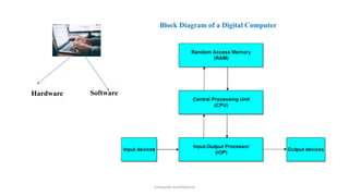
The document discusses computer architecture and describes the basic components of a computer. It discusses the instruction cycle which involves fetching instructions from memory, decoding them, reading the effective address from memory, and executing the instruction. The basic computer has three types of instructions - memory reference, register reference, and input/output. Memory reference instructions refer to memory addresses and use direct or indirect addressing. Register reference instructions perform operations on registers. Input/output instructions are used for communication with external devices. The instruction cycle is then completed by fetching and executing the next instruction.


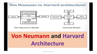
![Types of Architecture
• Von Neumann Architecture [Princeton Architecture]
• Harvard Architecture
Computer Architecture](https://image.slidesharecdn.com/unit1-computerarchitecture1-211031100705/85/Unit-1-computer-architecture-1-5-320.jpg)


![INTRODUCTION
• Every different processor type has its own design (different registers, buses, microoperations, machine
instructions, etc)
• Modern processor is a very complex device
• It contains
• Many registers
• Multiple arithmetic units, for both integer and floating point calculations
• The ability to pipeline several consecutive instructions to speed execution
• Etc.
• However, to understand how processors work, we will start with a simplified processor model
• This is similar to what real processors were like ~25 years ago
• M. Morris Mano introduces a simple processor model he calls the Basic Computer
• We will use this to introduce processor organization and the relationship of the RTL model to the higher
level computer processor
[In digital circuit design, register-transfer level (RTL) is a design abstraction which models a synchronous digital circuit
in terms of the flow of digital signals (data) between hardware registers, and the logical operations performed on those
signals.]
Computer Architecture](https://image.slidesharecdn.com/unit1-computerarchitecture1-211031100705/85/Unit-1-computer-architecture-1-20-320.jpg)


![Instruction Cycle
• Initially, the program counter PC is loaded with the address of the first instruction in the program.
The sequence counter SC is cleared to 0, providing a decoded timing signal To.
• After each clock pulse, SC is incremented by one, so that the timing signals go through a sequence
T0, T1, T2, and so on. The microoperations for the fetch and decode phases can be specified by
the following register transfer statements.
• T0: AR <- PC
• T1: IR <-M[AR], PC <- PC + 1
• T2: D0, ••• , D7 <-Decode IR(12-14), AR <---IR(0-11), 1 <---IR(l5)
• Since only AR is connected to the address inputs of memory, it is necessary to transfer the
address from PC to AR during the clock transition associated with timing signal T0
• 1.The content of PC is placed onto the bus by setting the bus selection inputs S2S1S0 ie)010
• 2. The content of the bus is transferred to AR by enabling the LD input of AR
Computer Architecture](https://image.slidesharecdn.com/unit1-computerarchitecture1-211031100705/85/Unit-1-computer-architecture-1-46-320.jpg)


![Type of Instruction and Addressing
During time T3, the control unit determines if this is a memory-reference, register-
reference or input/output instruction.
If D7=1,then it should be register reference or I/O reference instruction depending
on I bit
-if D7 ≠0,it is a memory-reference instruction, opcode must be 000 through 011 the
I bit will determine direct or indirect addressing.
• The four separate paths are:
D7’IT3: AR ¬ M[AR]
D7’I’T3: Nothing
D7I’T3: Execute a register-reference instruction
D7IT3: Execute an input-output instruction
Computer Architecture](https://image.slidesharecdn.com/unit1-computerarchitecture1-211031100705/85/Unit-1-computer-architecture-1-50-320.jpg)


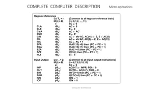
![COMPLETE COMPUTER DESCRIPTION
Fetch
Decode
Indirect
Interrupt
Memory-Reference
AND
ADD
LDA
STA
BUN
BSA
ISZ
RT0:
RT1:
RT2:
D7IT3:
RT0:
RT1:
RT2:
D0T4:
D0T5:
D1T4:
D1T5:
D2T4:
D2T5:
D3T4:
D4T4:
D5T4:
D5T5:
D6T4:
D6T5:
D6T6:
AR PC
IR M[AR], PC PC + 1
D0, ..., D7 Decode IR(12 ~ 14),
AR IR(0 ~ 11), I IR(15)
AR M[AR]
R 1
AR 0, TR PC
M[AR] TR, PC 0
PC PC + 1, IEN 0, R 0, SC 0
DR M[AR]
AC AC DR, SC 0
DR M[AR]
AC AC + DR, E Cout, SC 0
DR M[AR]
AC DR, SC 0
M[AR] AC, SC 0
PC AR, SC 0
M[AR] PC, AR AR + 1
PC AR, SC 0
DR M[AR]
DR DR + 1
M[AR] DR, if(DR=0) then (PC PC + 1),
SC 0
T0T1T2(IEN)(FGI + FGO):
Computer Architecture](https://image.slidesharecdn.com/unit1-computerarchitecture1-211031100705/85/Unit-1-computer-architecture-1-63-320.jpg)

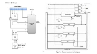
![CONTROL OF REGISTERS AND MEMORY
Scan all of the register transfer statements that change the content of AR:
LD(AR) = R'T0 + R'T2 + D'7IT3
CLR(AR) = RT0
INR(AR) = D5T4
Address Register; AR
R’T0: AR PC LD(AR)
R’T2: AR IR(0-11) LD(AR)
D’7IT3: AR M[AR] LD(AR)
RT0: AR 0 CLR(AR)
D5T4: AR AR + 1 INR(AR)
Design of Basic Computer
AR
LD
INR
CLR
Clock
To bus
12
From bus
12
D'
I
T
T
R
T
D
T
7
3
2
0
4
Computer Architecture](https://image.slidesharecdn.com/unit1-computerarchitecture1-211031100705/85/Unit-1-computer-architecture-1-66-320.jpg)