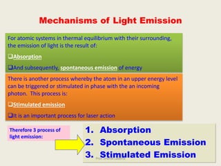
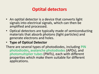
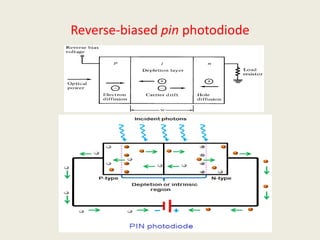
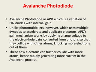
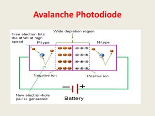
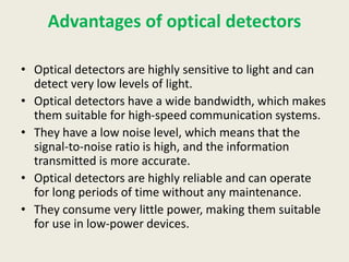
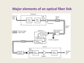
Optical detectors convert received light signals into electrical signals. PIN photodiodes are commonly used and have an intrinsic layer between the p-region and n-region to widen the depletion zone. Avalanche photodiodes provide internal gain through collisions that generate more electrons. Optical detectors have advantages like high sensitivity, wide bandwidth, low noise and reliability but also have disadvantages like limited dynamic range and sensitivity to temperature changes.
![Attenuation
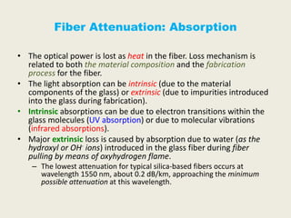
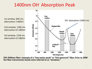
• Signal attenuation (loss) is a measure of power received
with respect to power sent.
• Silica-based glass fibers have losses of about 0.2 dB/km
(i.e. 95% launched power remains after 1 km of fiber
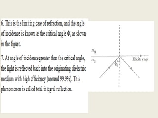
transmission).
• Drawback on fibers: if only a little section develops a high
attenuation, the whole fiber is lost.
• Signal attenuation within optical fibers is usually
expressed in the logarithmic unit of the decibel (dB).
• The decibel is defined for a particular optical wavelength
as the ratio of the output optical power Po from the fiber
to the input optical power Pi into the fiber (Po Pi)
Loss[dB]= -10×log10
Pout
Pin
æ
è
ç
ö
ø
÷](https://image.slidesharecdn.com/unit5mwoc-231207052656-65b66ceb/85/B-Tech-ECE-IV-Year-I-Sem-MWOC-UNIT-5-Optical-CommunicationsUNIT-5-MWOC-pptx-23-320.jpg)