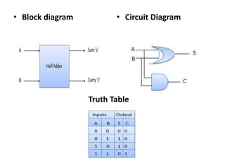
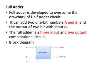
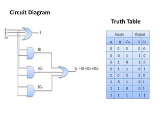
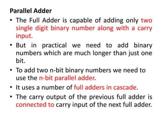
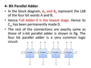
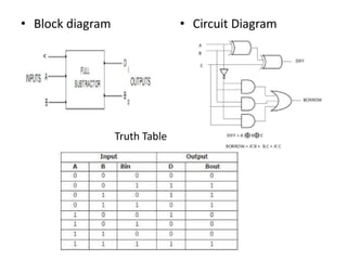
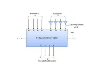
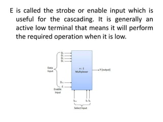
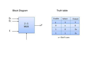
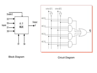
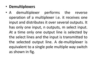
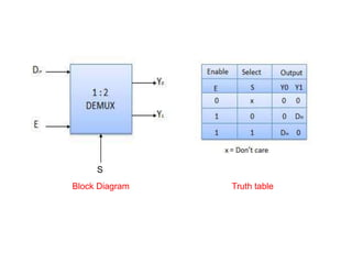
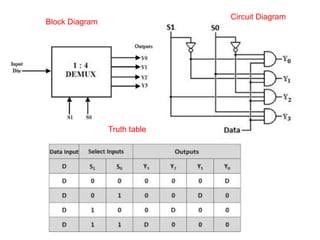
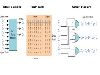
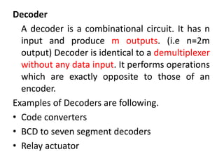
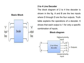
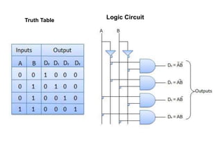
Combinational Circuits
Combinational circuit is a circuit in which we
combine the different gates in the circuit.
for example adder, subtractor, encoder, decoder,
multiplexer and demultiplexer.
Some of the characteristics of combinational
circuits are following :
•The output of combinational circuit at any instant
of time depends only on the levels present at input
terminals.
•The combinational circuit do not use any memory.
• The previous state of input does not have any
effect on the present state of the circuit.
• A combinational circuit can have an n number
of inputs and m number of outputs.
• Block diagram
Half Adder
• Half adder is a combinational logic circuit with
two inputs and two outputs.
• The half adder circuit is designed to add two
single bit binary number A and B.
• It is the basic building block for addition of two
single bit numbers.
• This circuit has two outputs carry and sum.
• Block diagram • Circuit Diagram
Truth Table
Full Adder
• Full adder is developed to overcome the
drawback of Half Adder circuit.
• It can add two one-bit numbers A and B, and
the output of two bit with input cin.
• The full adder is a three input and two output
combinational circuit.
• Block diagram
Circuit Diagram
Truth Table
Parallel Adder
• The Full Adder is capable of adding only two
single digit binary number along with a carry
input.
• But in practical we need to add binary
numbers which are much longer than just one
bit.
• To add two n-bit binary numbers we need to
use the n-bit parallel adder.
• It uses a number of full adders in cascade.
• The carry output of the previous full adder is
connected to carry input of the next full adder.
4- Bit Parallel Adder
• In the block diagram, A0 and B0 represent the LSB
of the four bit words A and B.
• Hence Full Adder-0 is the lowest stage. Hence its
Cin has been permanently made 0.
• The rest of the connections are exactly same as
those of n-bit parallel adder is shown in fig. The
four bit parallel adder is a very common logic
circuit.
• Half Subtractor
• Half subtractor is a combination circuit with
two inputs and two outputs (difference and
borrow).
• It produces the difference between the two
binary bits at the input as a difference(i.e A-B).
• It also produces an output (Borrow) to
indicate if a 1 has been borrowed.
• In the subtraction (A-B), A is called as
Minuend bit and B is called as Subtrahend bit.
• Block Diagram • Circuit Diagram
Truth Table
Full Subtractor
• The disadvantage of a half subtractor is
overcome by full subtractor.
• The full subtractor is a combinational circuit
with three inputs A,B,C and two output
Difference and Borrow.
• The input are A is the 'minuend', B is
'subtrahend', C is the 'borrow' and produced
by the previous stage .
• D is the difference output and B is the borrow
output.
• Block diagram • Circuit Diagram
Truth Table
Parallel Subtractor
The subtraction can be carried out by taking the
1's or 2's complement of the number to be
subtracted.
For example we can perform the subtraction (A-
B) by adding either 1's or 2's complement of B
to A.
That means we can use a binary adder to
perform the binary subtraction.
4 Bit Parallel Subtractor
• The number to be subtracted (B) is first passed
through inverters to obtain its 1's
complement.
• The 4-bit adder then adds A and 2's
complement of B to produce the subtraction.
S3 S2 S1 S0 represents the result of binary
subtraction (A-B) and carry output Cout
represents the polarity of the result.
• If A > B then Cout = 0 and the result of binary
form (A-B) then Cout = 1 and the result is in the
2's complement form.
Multiplexers
• Multiplexer is a special type of combinational
circuit. There are n-data inputs, one output
and m select inputs with 2m = n. It is a digital
circuit which selects one of the n data inputs
and routes it to the output. The selection of
one of the n inputs is done by the selected
inputs. Depending on the digital code applied
at the selected inputs, one out of n data
sources is selected and transmitted to the
single output Y.
E is called the strobe or enable input which is
useful for the cascading. It is generally an
active low terminal that means it will perform
the required operation when it is low.
Multiplexers come in multiple variations
• 2 : 1 multiplexer
• 4 : 1 multiplexer
• 8 :1 multiplexer
• 16 : 1 multiplexer
• 32 : 1 multiplexer
Block Diagram Truth table
Block Diagram Circuit Diagram
• Demultiplexers
• A demultiplexer performs the reverse
operation of a multiplexer i.e. it receives one
input and distributes it over several outputs. It
has only one input, n outputs, m select input.
At a time only one output line is selected by
the select lines and the input is transmitted to
the selected output line. A de-multiplexer is
equivalent to a single pole multiple way switch
as shown in fig.
Demultiplexers comes in multiple variations.
• 1 : 2 demultiplexer
• 1 : 4 demultiplexer
• 1 : 8 demultiplexer
• 1 : 16 demultiplexer
• 1 : 32 demultiplexer
Block Diagram Truth table
S
Block Diagram
Truth table
Circuit Diagram
Encoder
• Encoder is a combinational circuit which is
designed to perform the inverse operation of
the decoder.
• An encoder has n number of input lines and m
number of output lines.
• An encoder produces an m bit binary code
corresponding to the digital input number.
• The encoder accepts an n input digital word
and converts it into an m bit another digital
word.
Examples of Encoders are following.
•Priority encoders
•Decimal to BCD encoder
•Octal to binary encoder
•Hexadecimal to binary encoder
Block diagram
Priority encoder
4:2 Encoder Circuit
Block Diagram Truth Table Circuit Diagram
Decoder
A decoder is a combinational circuit. It has n
input and produce m outputs. (i.e n=2m
output) Decoder is identical to a demultiplexer
without any data input. It performs operations
which are exactly opposite to those of an
encoder.
Examples of Decoders are following.
• Code converters
• BCD to seven segment decoders
• Relay actuator
2 to 4 Line Decoder
The block diagram of 2 to 4 line decoder is
shown in the fig. A and B are the two inputs
where D through D are the four outputs. Truth
table explains the operations of a decoder. It
shows that each output is 1 for only a specific
combination of inputs.
Block diagram
Basic Block
Logic Circuit
Truth Table

Combinational circuits r011

  • 1.
    Combinational Circuits Combinational circuitis a circuit in which we combine the different gates in the circuit. for example adder, subtractor, encoder, decoder, multiplexer and demultiplexer. Some of the characteristics of combinational circuits are following : •The output of combinational circuit at any instant of time depends only on the levels present at input terminals. •The combinational circuit do not use any memory.
  • 2.
    • The previousstate of input does not have any effect on the present state of the circuit. • A combinational circuit can have an n number of inputs and m number of outputs. • Block diagram
  • 3.
    Half Adder • Halfadder is a combinational logic circuit with two inputs and two outputs. • The half adder circuit is designed to add two single bit binary number A and B. • It is the basic building block for addition of two single bit numbers. • This circuit has two outputs carry and sum.
  • 4.
    • Block diagram• Circuit Diagram Truth Table
  • 5.
    Full Adder • Fulladder is developed to overcome the drawback of Half Adder circuit. • It can add two one-bit numbers A and B, and the output of two bit with input cin. • The full adder is a three input and two output combinational circuit. • Block diagram
  • 6.
  • 7.
    Parallel Adder • TheFull Adder is capable of adding only two single digit binary number along with a carry input. • But in practical we need to add binary numbers which are much longer than just one bit. • To add two n-bit binary numbers we need to use the n-bit parallel adder. • It uses a number of full adders in cascade. • The carry output of the previous full adder is connected to carry input of the next full adder.
  • 8.
    4- Bit ParallelAdder • In the block diagram, A0 and B0 represent the LSB of the four bit words A and B. • Hence Full Adder-0 is the lowest stage. Hence its Cin has been permanently made 0. • The rest of the connections are exactly same as those of n-bit parallel adder is shown in fig. The four bit parallel adder is a very common logic circuit.
  • 9.
    • Half Subtractor •Half subtractor is a combination circuit with two inputs and two outputs (difference and borrow). • It produces the difference between the two binary bits at the input as a difference(i.e A-B). • It also produces an output (Borrow) to indicate if a 1 has been borrowed. • In the subtraction (A-B), A is called as Minuend bit and B is called as Subtrahend bit.
  • 10.
    • Block Diagram• Circuit Diagram Truth Table
  • 11.
    Full Subtractor • Thedisadvantage of a half subtractor is overcome by full subtractor. • The full subtractor is a combinational circuit with three inputs A,B,C and two output Difference and Borrow. • The input are A is the 'minuend', B is 'subtrahend', C is the 'borrow' and produced by the previous stage . • D is the difference output and B is the borrow output.
  • 12.
    • Block diagram• Circuit Diagram Truth Table
  • 13.
    Parallel Subtractor The subtractioncan be carried out by taking the 1's or 2's complement of the number to be subtracted. For example we can perform the subtraction (A- B) by adding either 1's or 2's complement of B to A. That means we can use a binary adder to perform the binary subtraction.
  • 14.
    4 Bit ParallelSubtractor • The number to be subtracted (B) is first passed through inverters to obtain its 1's complement. • The 4-bit adder then adds A and 2's complement of B to produce the subtraction. S3 S2 S1 S0 represents the result of binary subtraction (A-B) and carry output Cout represents the polarity of the result. • If A > B then Cout = 0 and the result of binary form (A-B) then Cout = 1 and the result is in the 2's complement form.
  • 16.
    Multiplexers • Multiplexer isa special type of combinational circuit. There are n-data inputs, one output and m select inputs with 2m = n. It is a digital circuit which selects one of the n data inputs and routes it to the output. The selection of one of the n inputs is done by the selected inputs. Depending on the digital code applied at the selected inputs, one out of n data sources is selected and transmitted to the single output Y.
  • 17.
    E is calledthe strobe or enable input which is useful for the cascading. It is generally an active low terminal that means it will perform the required operation when it is low.
  • 18.
    Multiplexers come inmultiple variations • 2 : 1 multiplexer • 4 : 1 multiplexer • 8 :1 multiplexer • 16 : 1 multiplexer • 32 : 1 multiplexer
  • 19.
  • 20.
  • 21.
    • Demultiplexers • Ademultiplexer performs the reverse operation of a multiplexer i.e. it receives one input and distributes it over several outputs. It has only one input, n outputs, m select input. At a time only one output line is selected by the select lines and the input is transmitted to the selected output line. A de-multiplexer is equivalent to a single pole multiple way switch as shown in fig.
  • 22.
    Demultiplexers comes inmultiple variations. • 1 : 2 demultiplexer • 1 : 4 demultiplexer • 1 : 8 demultiplexer • 1 : 16 demultiplexer • 1 : 32 demultiplexer
  • 23.
  • 24.
  • 25.
    Encoder • Encoder isa combinational circuit which is designed to perform the inverse operation of the decoder. • An encoder has n number of input lines and m number of output lines. • An encoder produces an m bit binary code corresponding to the digital input number. • The encoder accepts an n input digital word and converts it into an m bit another digital word.
  • 26.
    Examples of Encodersare following. •Priority encoders •Decimal to BCD encoder •Octal to binary encoder •Hexadecimal to binary encoder Block diagram
  • 27.
  • 28.
    Block Diagram TruthTable Circuit Diagram
  • 29.
    Decoder A decoder isa combinational circuit. It has n input and produce m outputs. (i.e n=2m output) Decoder is identical to a demultiplexer without any data input. It performs operations which are exactly opposite to those of an encoder. Examples of Decoders are following. • Code converters • BCD to seven segment decoders • Relay actuator
  • 30.
    2 to 4Line Decoder The block diagram of 2 to 4 line decoder is shown in the fig. A and B are the two inputs where D through D are the four outputs. Truth table explains the operations of a decoder. It shows that each output is 1 for only a specific combination of inputs. Block diagram Basic Block
  • 31.