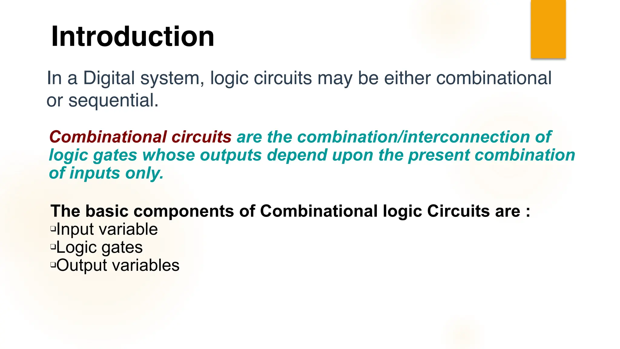
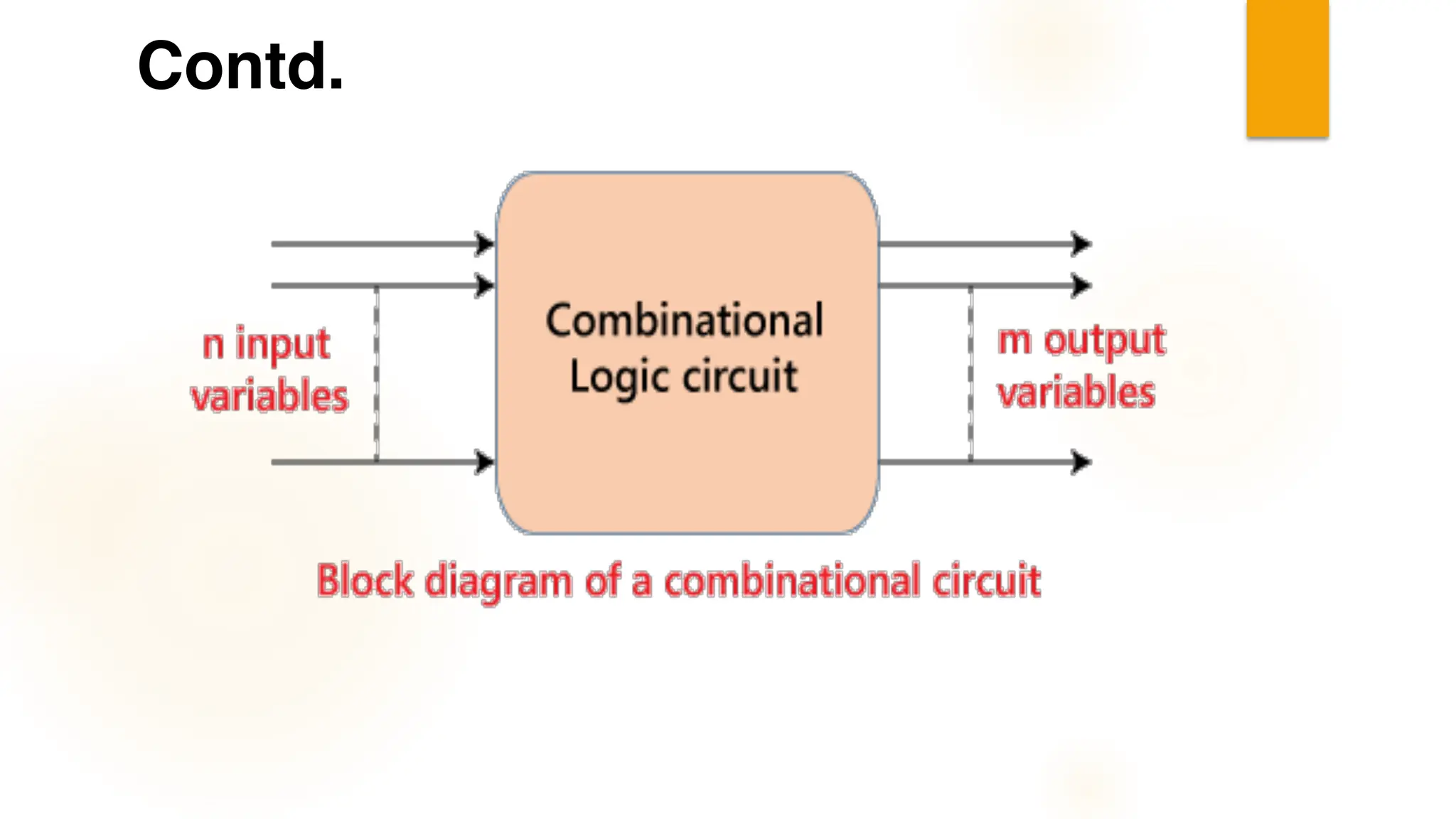
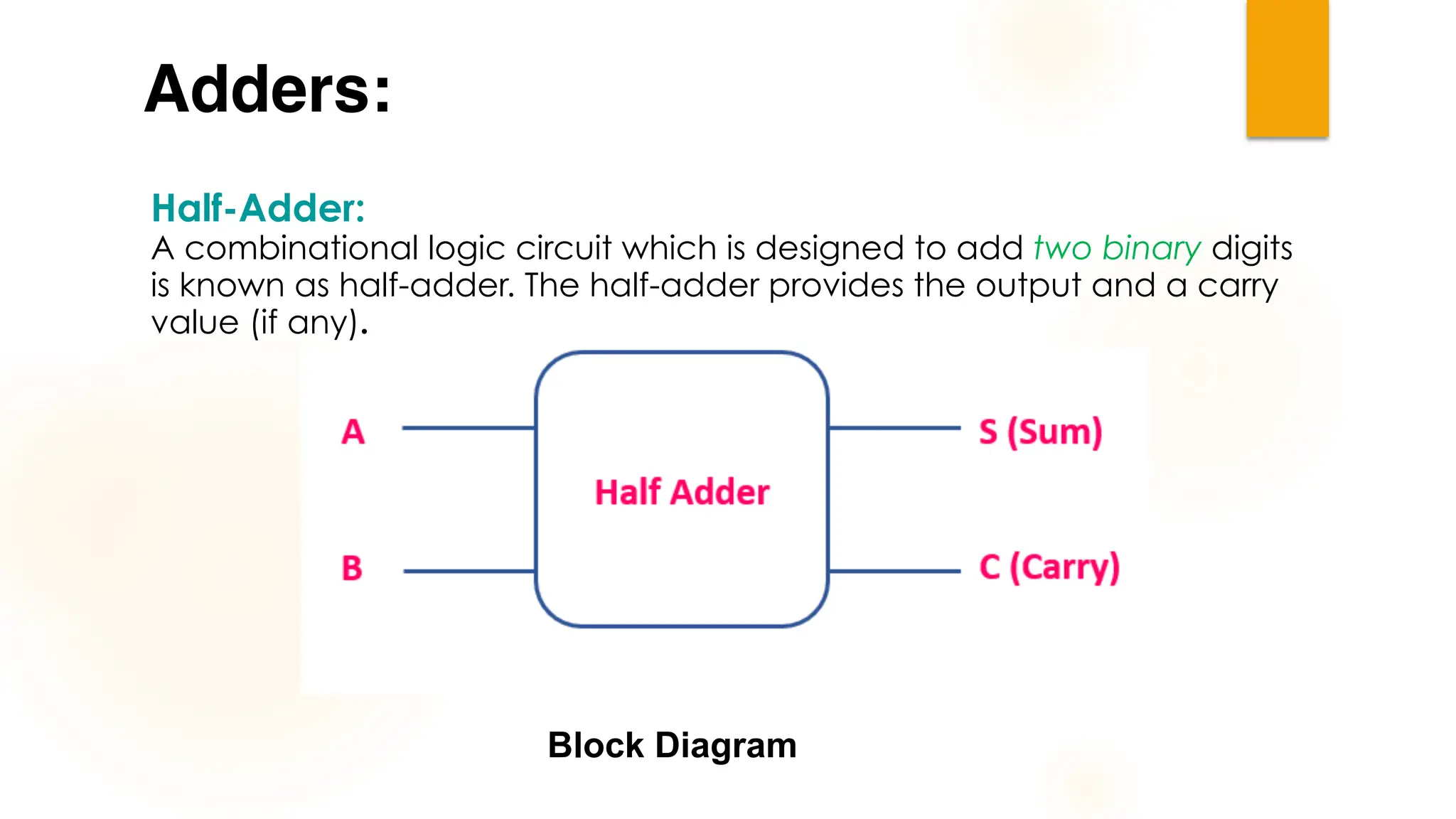
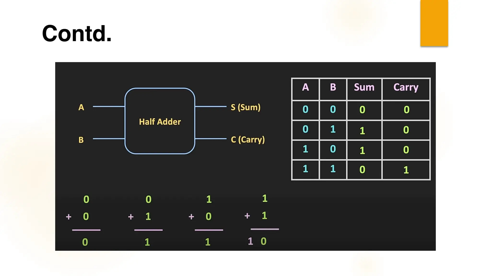
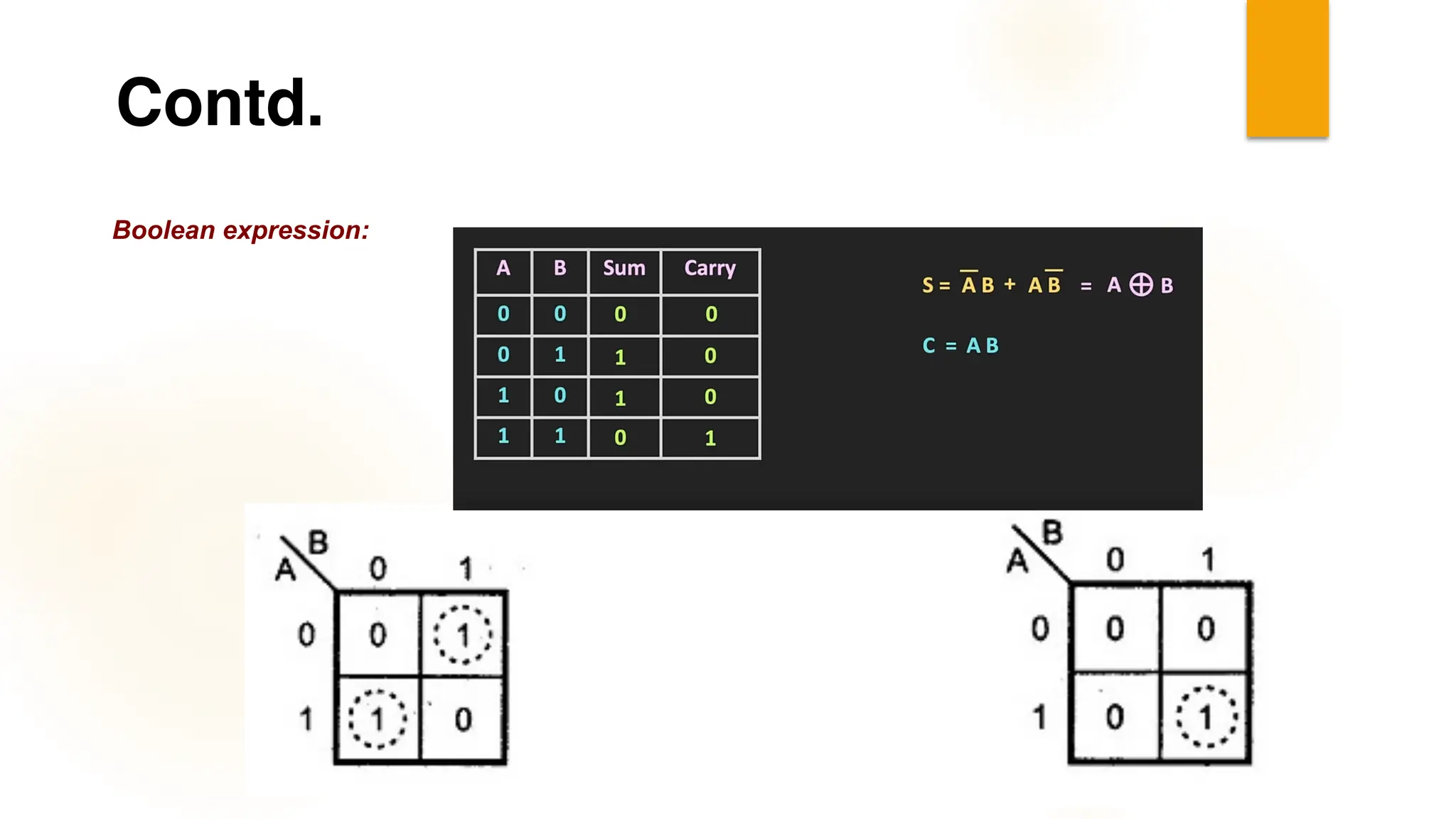
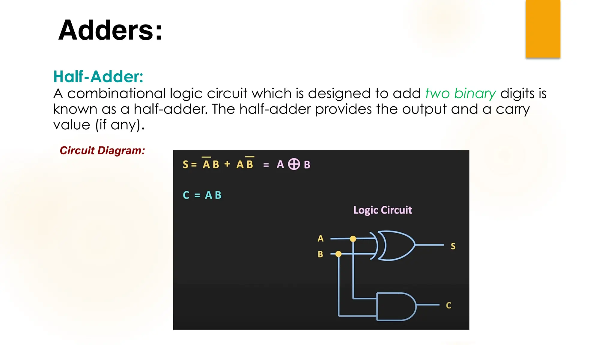
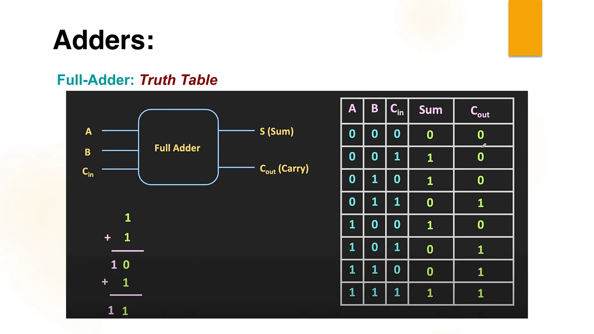
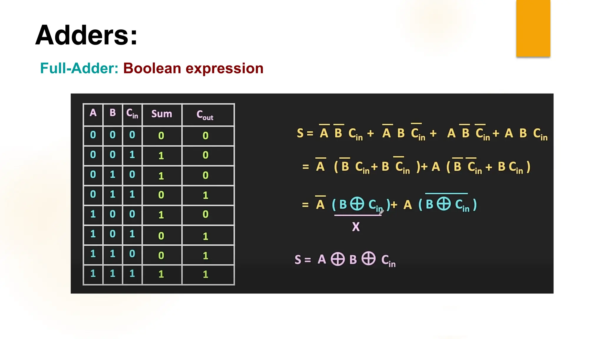
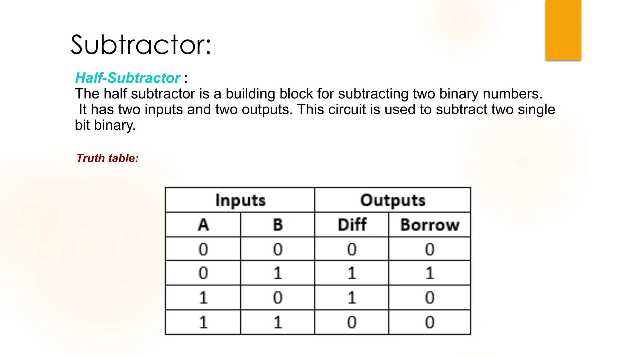
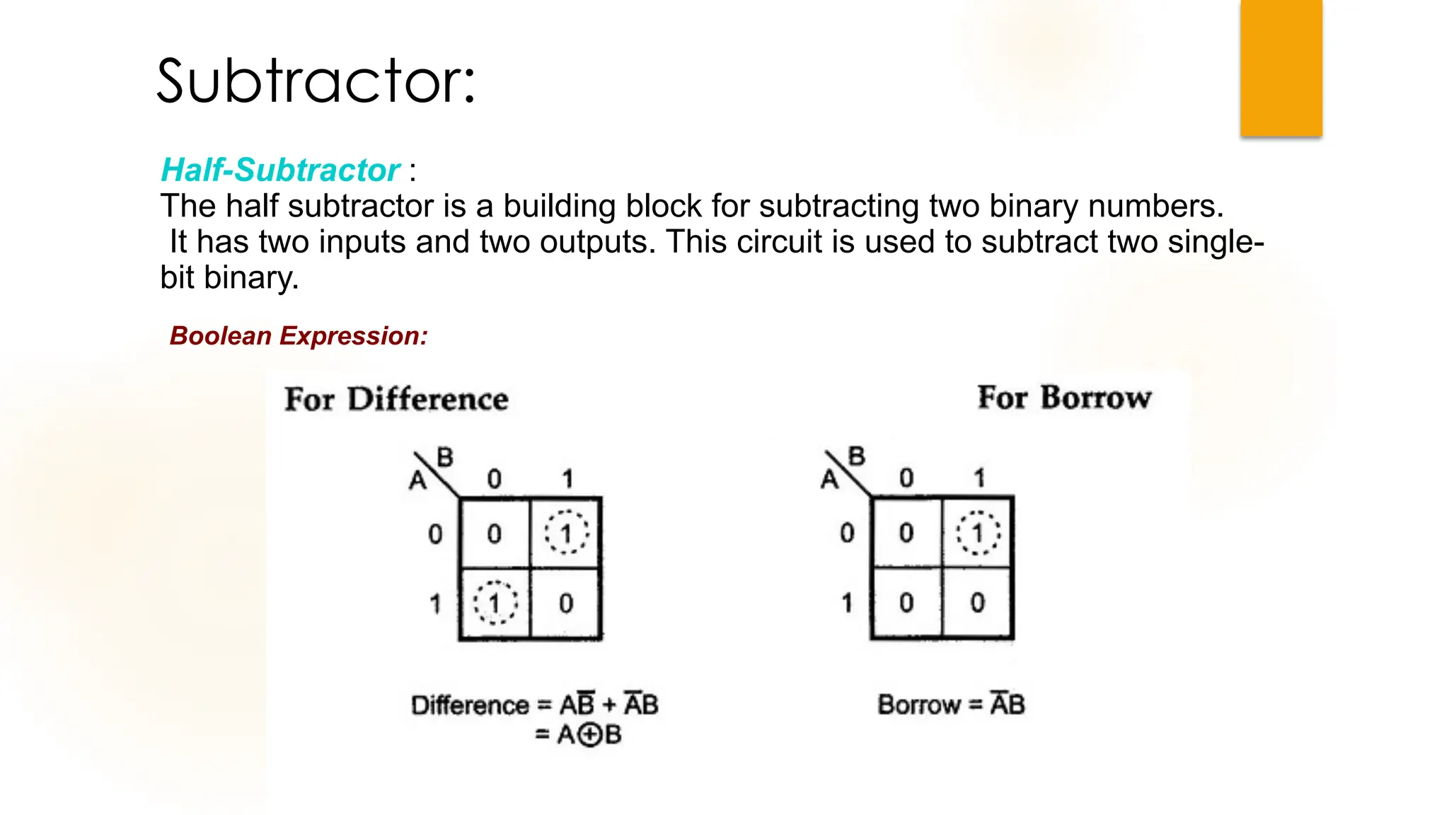
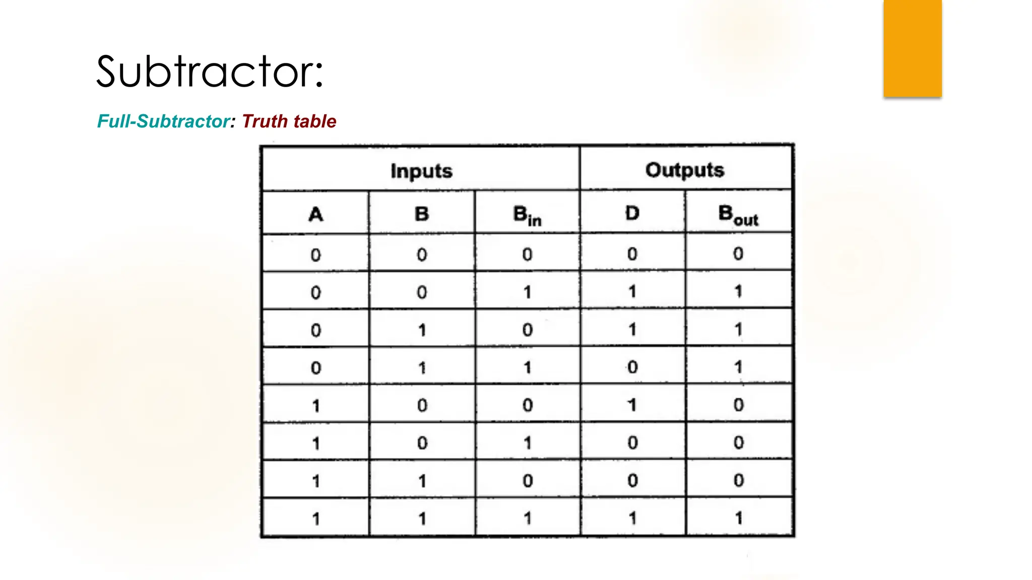
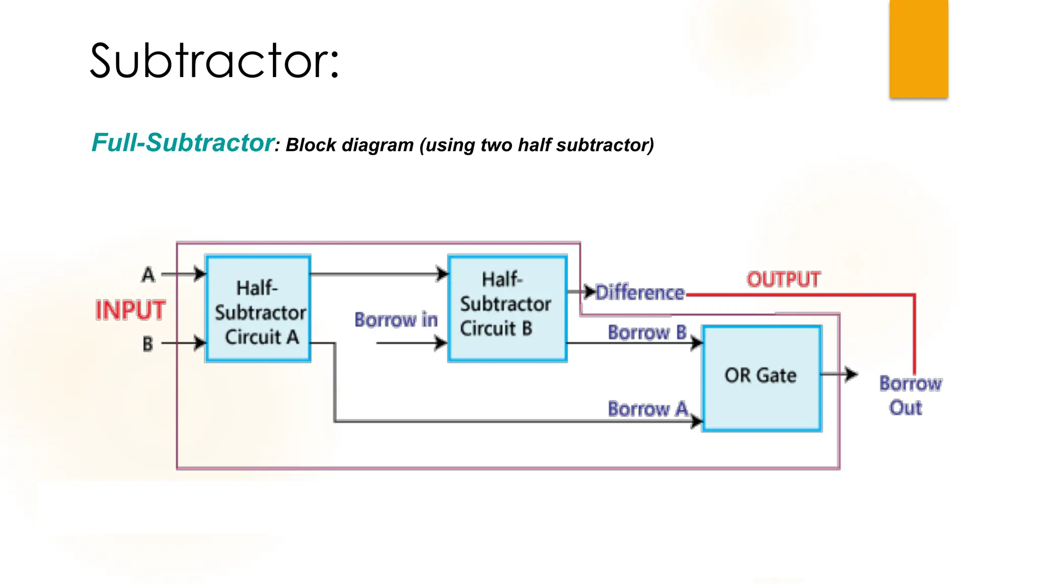
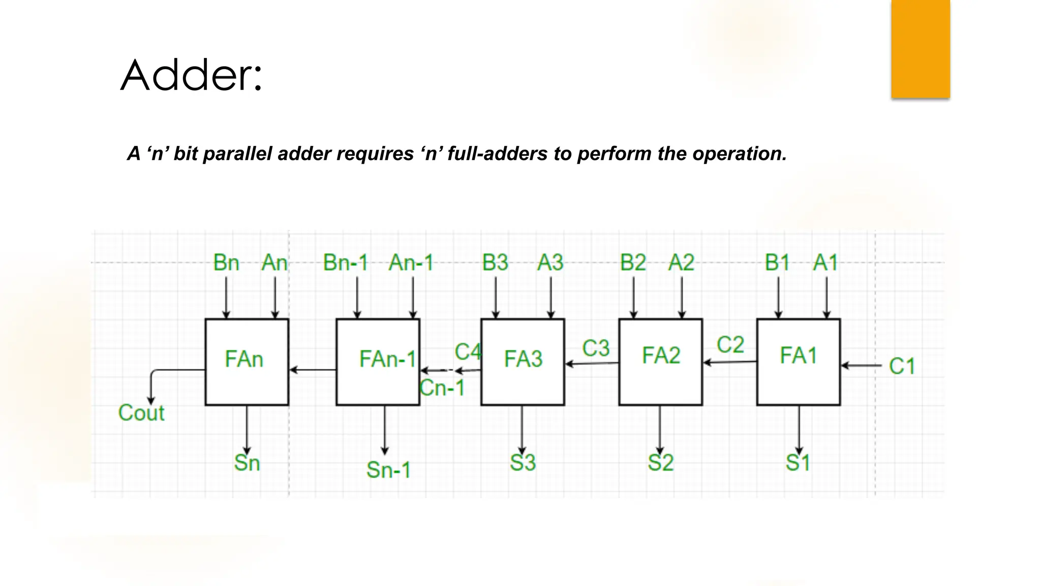
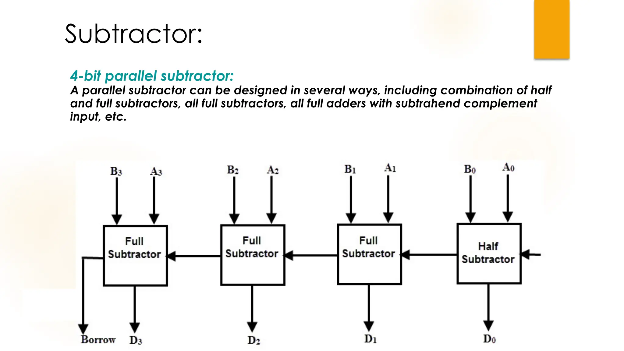
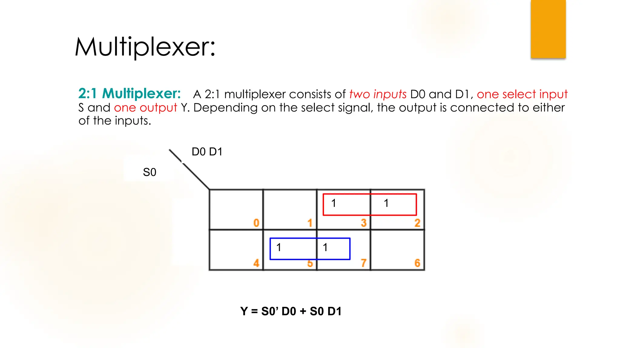
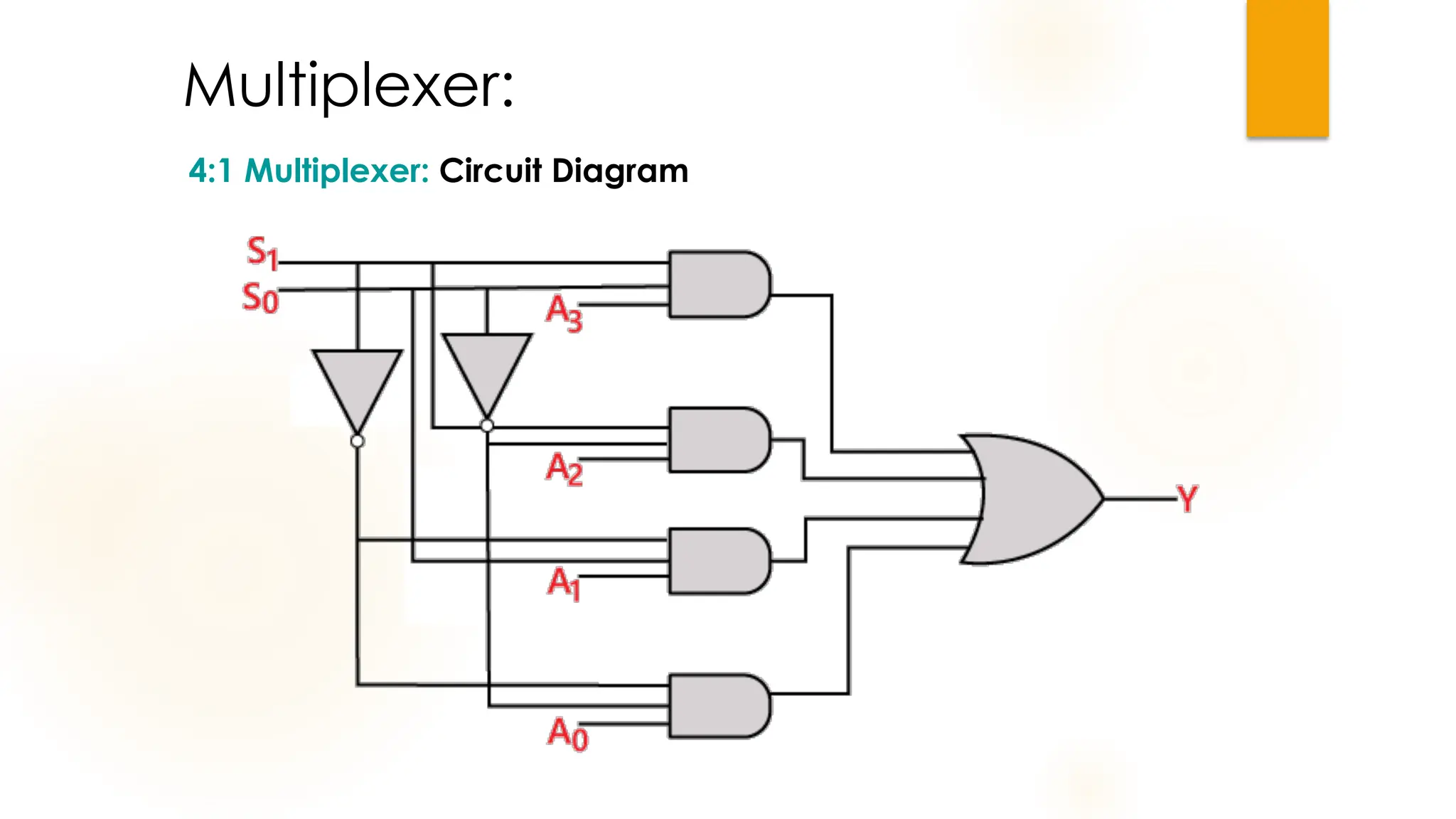
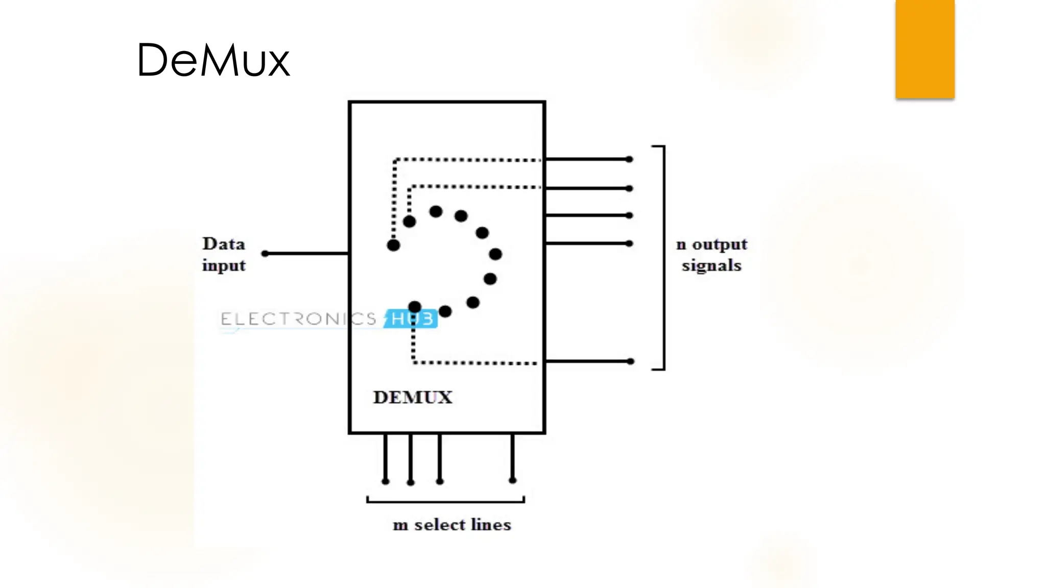
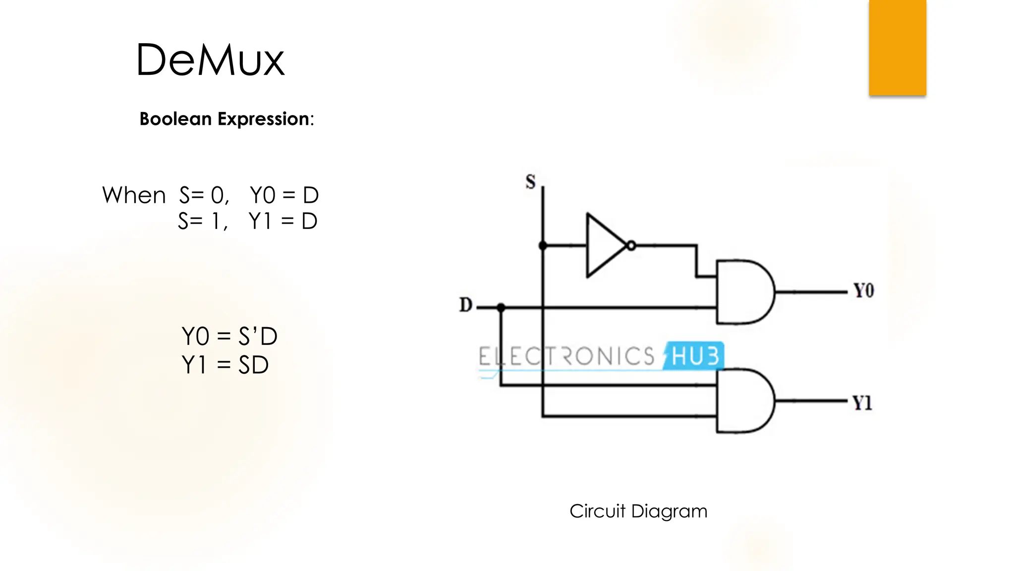
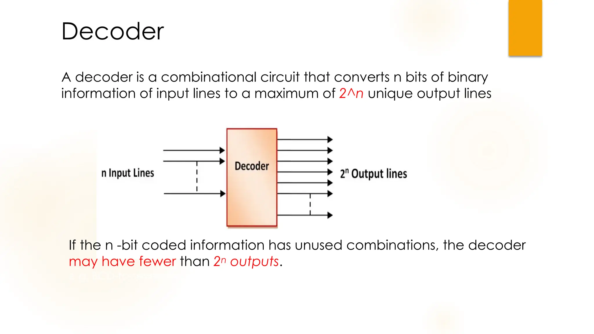
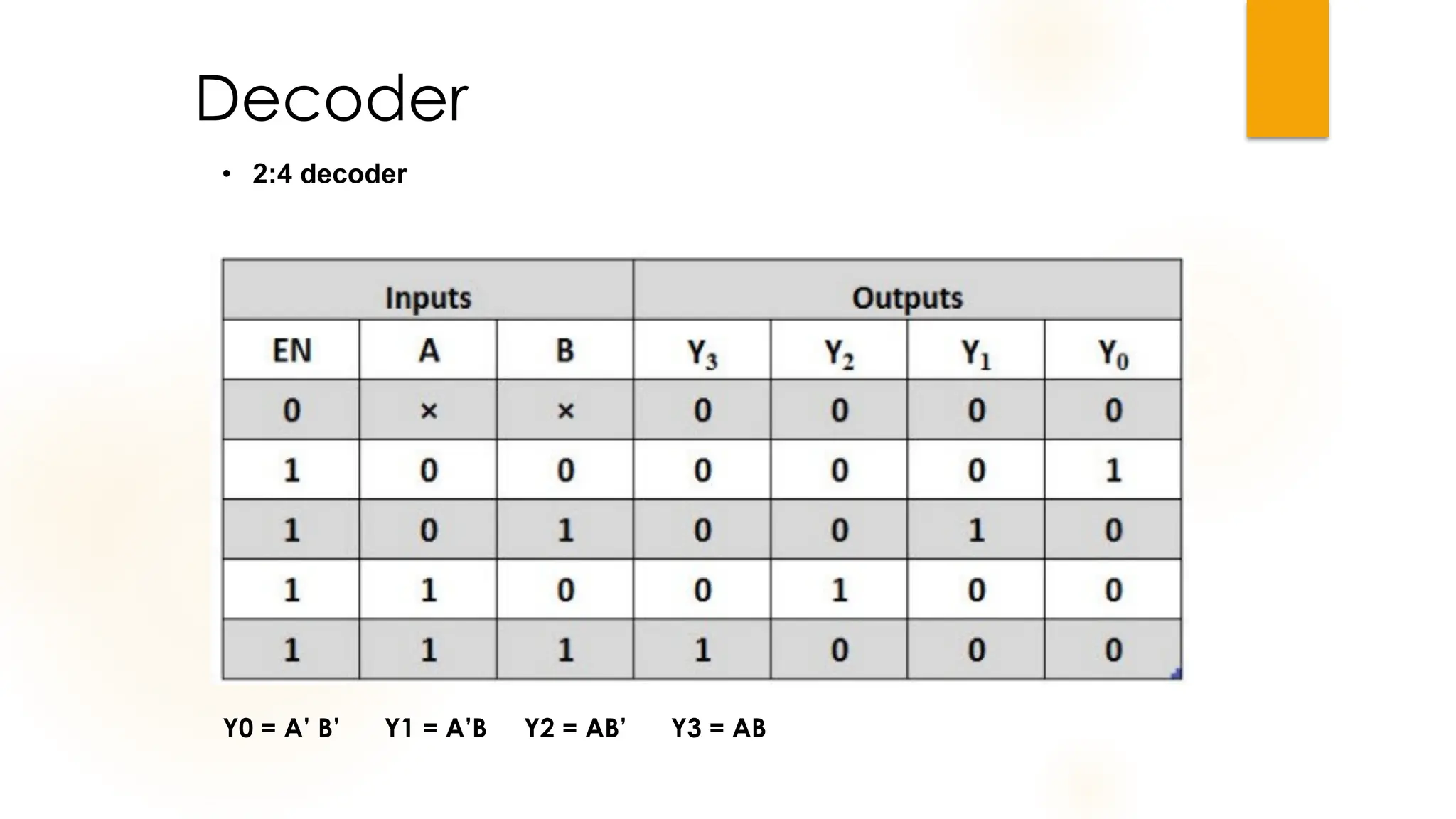
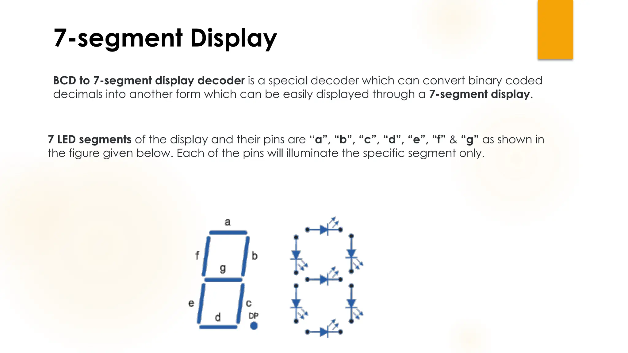
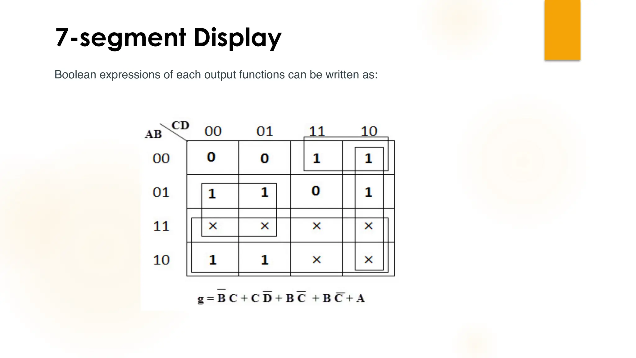
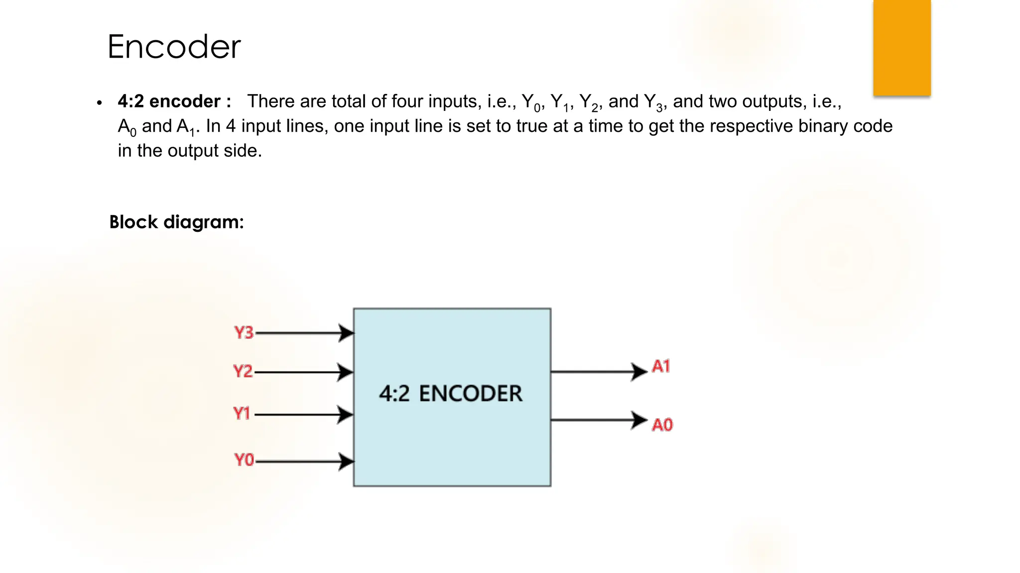
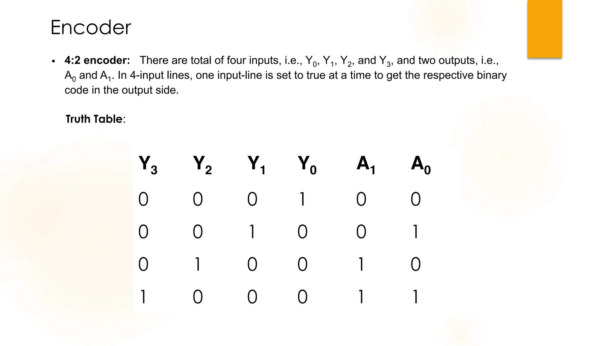
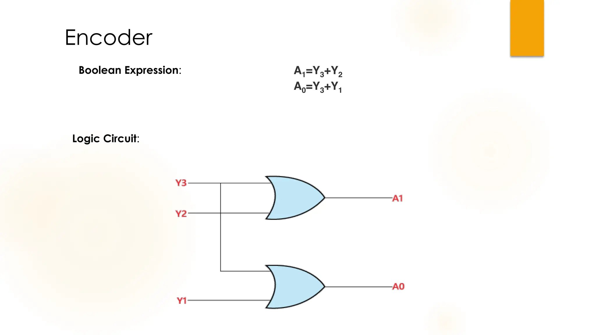
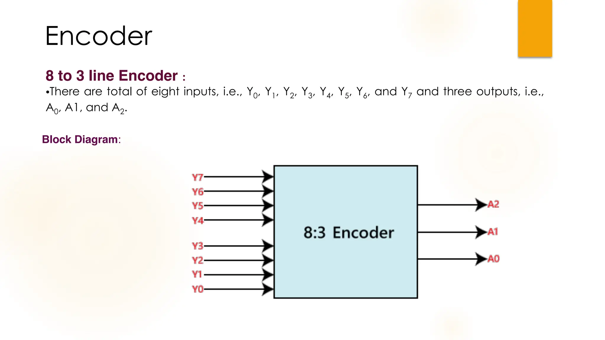
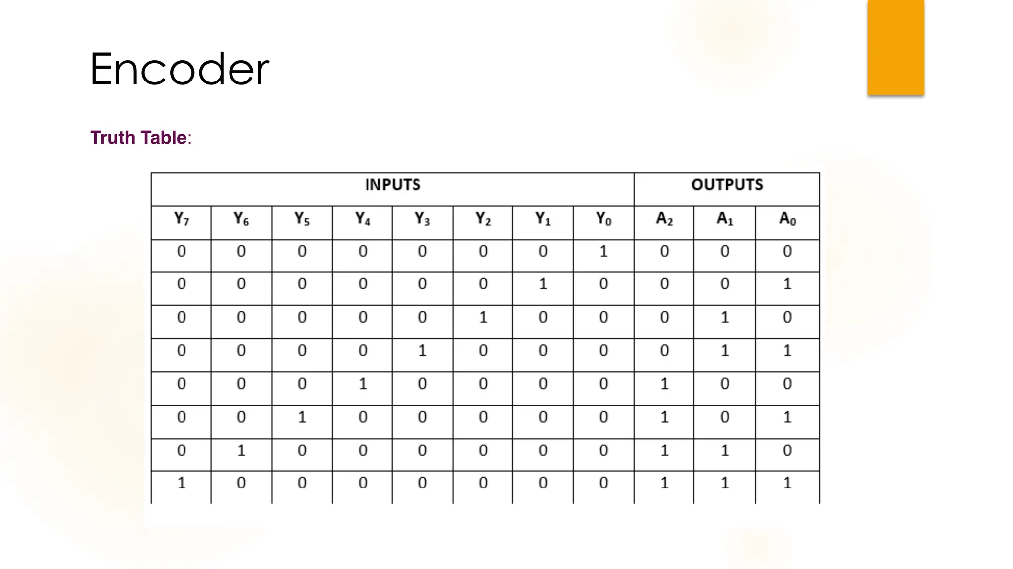
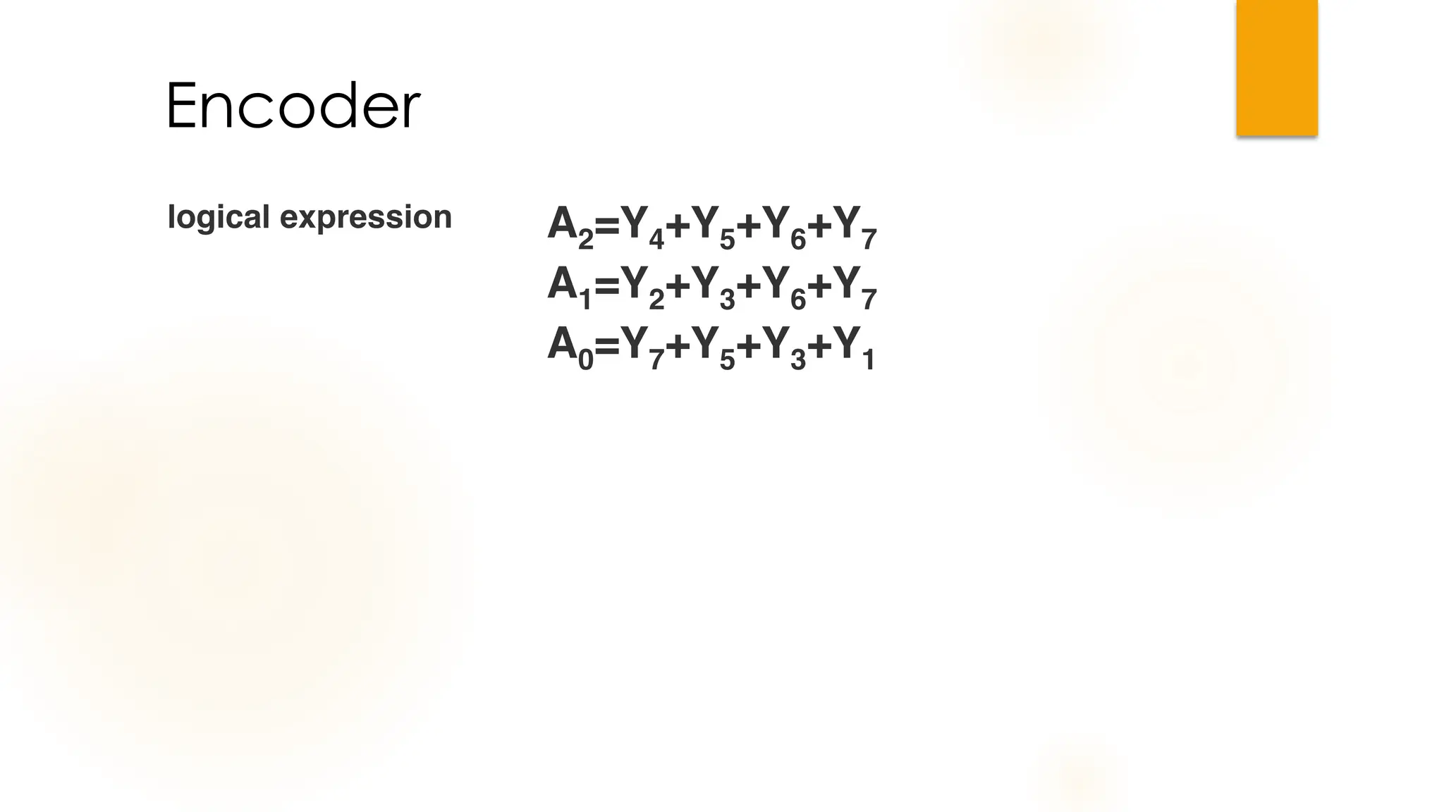
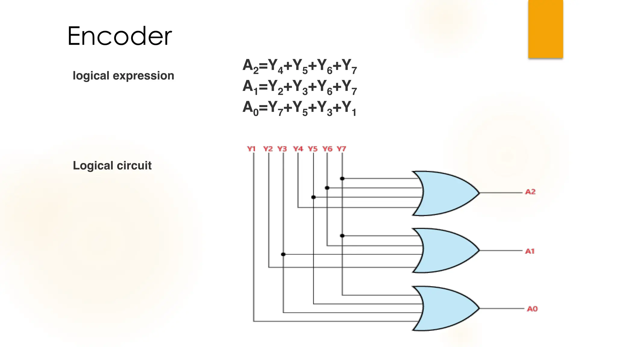
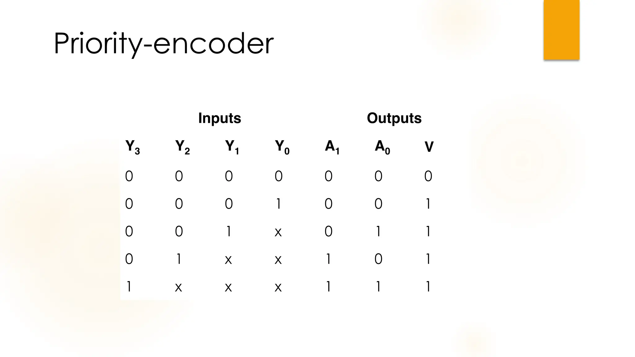
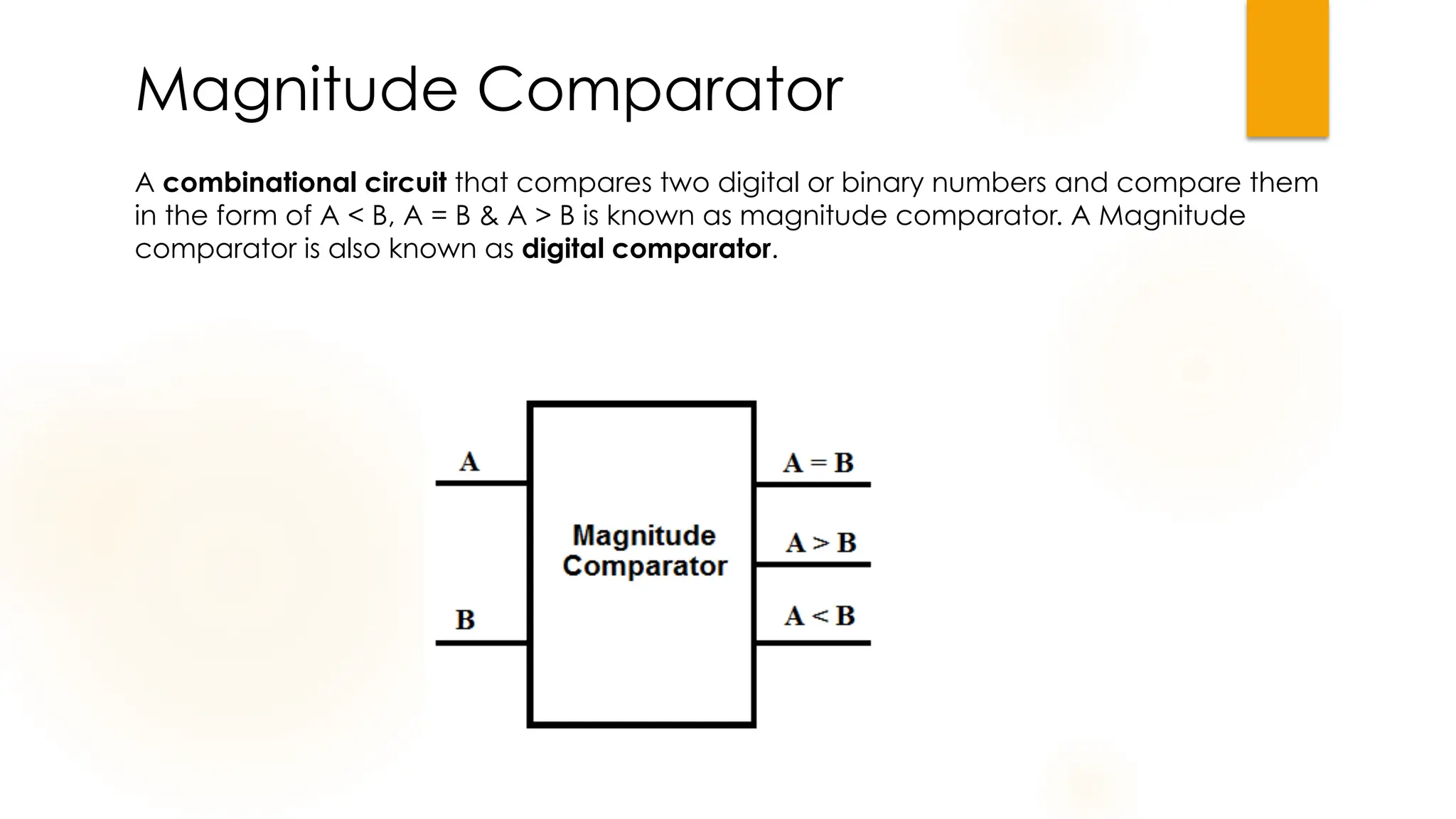
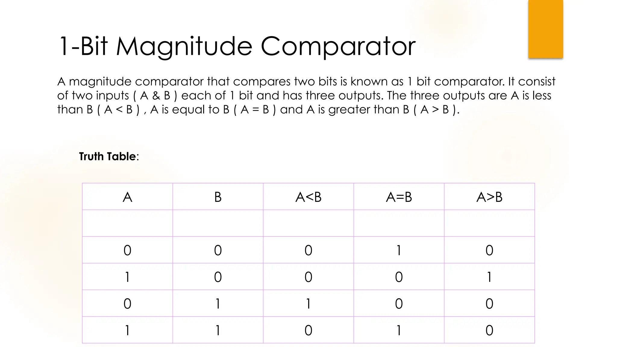
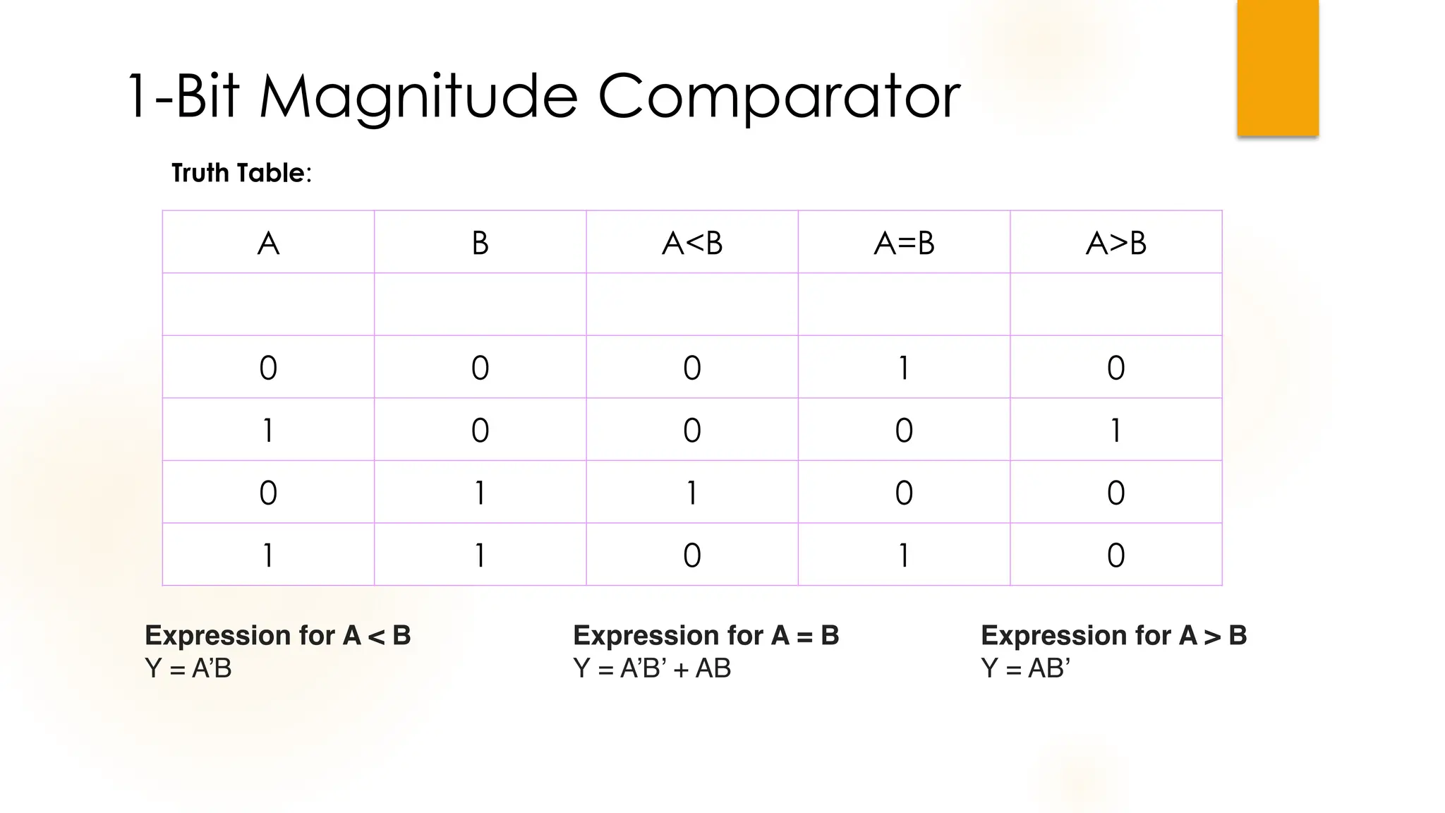
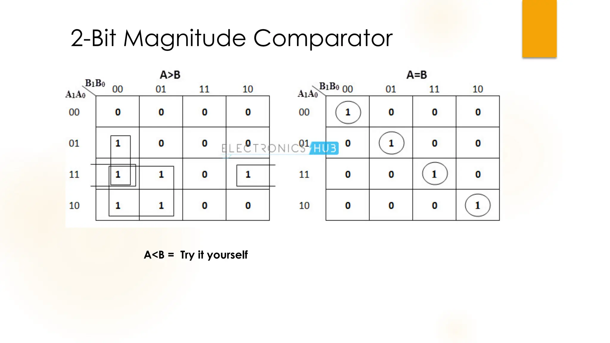
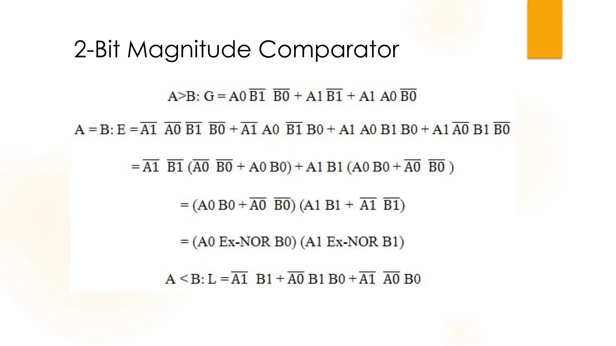
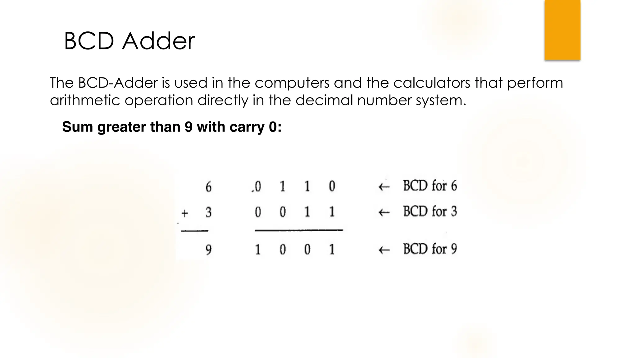
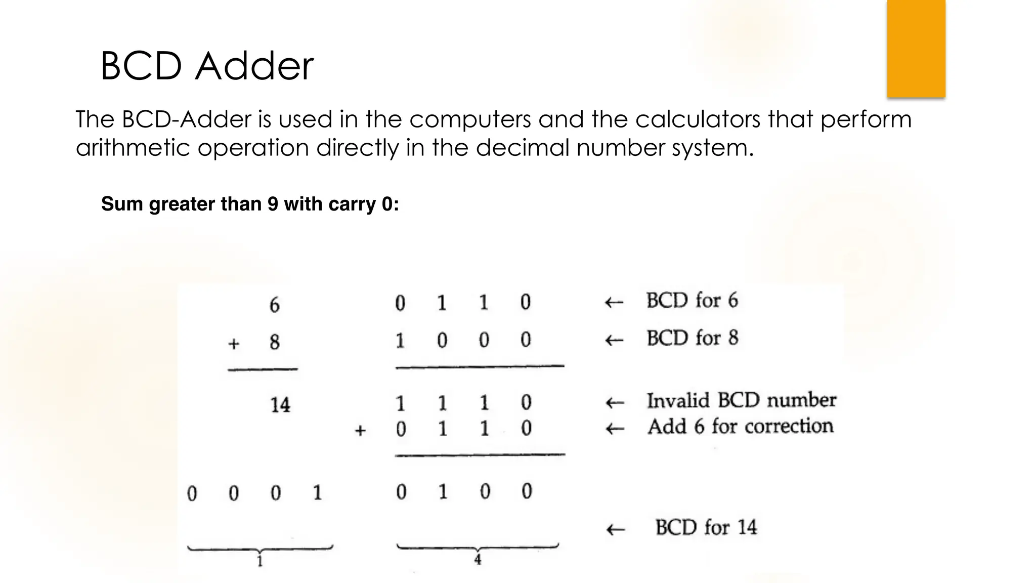
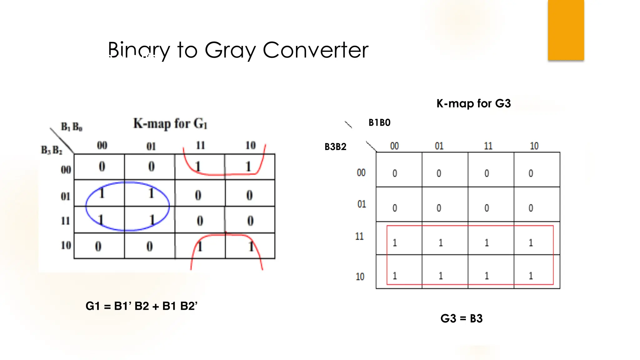
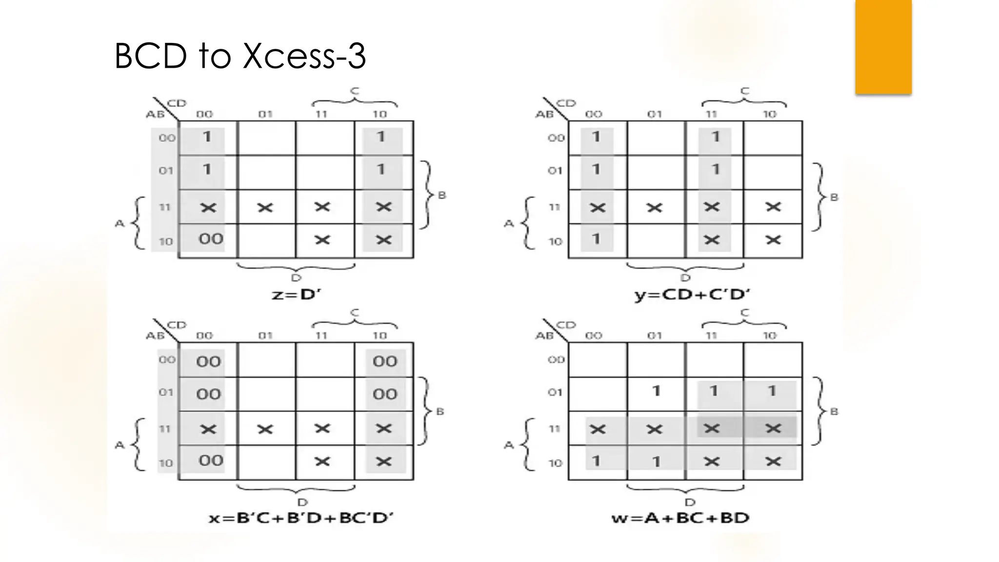
Digital Logic Circuits
Combinational Logic Circuits
UNIT - II
Learning Outcomes
• Explain the working of basic combinational circuits.
• Distinguish between the functions of different
combinational circuits.
• Build combinational circuits to perform a required
function.
In a Digital system, logic circuits may be either combinational
or sequential.
Combinational circuits are the combination/interconnection of
logic gates whose outputs depend upon the present combination
of inputs only.
The basic components of Combinational logic Circuits are :
❑Input variable
❑Logic gates
❑Output variables
Introduction
Contd.
Characteristics
❑ The output of a combinational circuit depends only on the
present input variables.
❑ These circuits have logic gates with no feedback path or
memory elements.
❑ Combinational circuits do not need any Clock pulse.
❑ A combinational circuit of ‘n’ input may have one output.
Classifications
Design Procedure
❑ Observe the problem definition.
❑ Determine the required number of inputs and outputs, and assign a
symbol to each variable.
❑ Make the truth table which establishes the relationship between input
and output variables,
❑ Determine the simplified boolean expression using K-map.
❑ Draw the logic diagram.
The design procedure involves the following steps:
Adders:
Block Diagram
Half-Adder:
A combinational logic circuit which is designed to add two binary digits
is known as half-adder. The half-adder provides the output and a carry
value (if any).
Contd.
Contd.
Boolean expression:
Adders:
Circuit Diagram:
Half-Adder:
A combinational logic circuit which is designed to add two binary digits is
known as a half-adder. The half-adder provides the output and a carry
value (if any).
Adders:
Block Diagram:
Full-Adder:
A combinational circuit designed to add three binary digits and produce
two outputs is known as full-adder. The full-adder circuit adds three binary
digits, where two are the inputs and one is the carry forward from the
previous addition.
Adders:
Full-Adder: Truth Table
Adders:
Full-Adder: Boolean expression
Adders:
Full-Adder: Boolean expression
Sum = m(1, 2, 4, 7) = A’B’Cin
+ A’BCin
’ + AB’Cin
’ + ABCin
= Cin
(A’B’ + AB) + Cin
’(A’B + AB’)
= Cin
(A x-nor B) + Cin
’(A’B + AB’)
= Cin
(A xor B)’ + Cin
’(A xor B)
= Cin
xor (A xor B)
Carry = m(3, 5, 6, 7) = A’BCin
+ AB’Cin
+ ABCin
’ + ABCin
= AB + BCin
+ Acin
= AB + Ciin
( A xor B)
Adders:
Full-Adder: Circuit Diagram
Adders:
Full-Adder: Circuit Diagram
Subtractor:
Block Diagram:
Half-Subtractor :
The half subtractor is a building block for subtracting two binary numbers.
It has two inputs and two outputs. This circuit is used to subtract two single
bit binary.
Certainly! Here is the revised text: "Subtractor:"
Subtractor:
Truth table:
Half-Subtractor :
The half subtractor is a building block for subtracting two binary numbers.
It has two inputs and two outputs. This circuit is used to subtract two single
bit binary.
Subtractor:
Boolean Expression:
Half-Subtractor :
The half subtractor is a building block for subtracting two binary numbers.
It has two inputs and two outputs. This circuit is used to subtract two single-
bit binary.
Subtractor:
Half-Subtractor : Circuit Diagram
Subtractor:
Full-Subtractor:
A Full Subtractor Circuit is a combinational circuit that performs a subtraction
between two bits, the circuit has three inputs and two outputs. The three
inputs are A, B and Bin, denote the minuend, subtrahend, and previous
borrow, respectively. The two outputs, D and Bout represent the difference
and output borrow, respectively.
Subtractor:
Full-Subtractor: Truth table
Subtractor:
Full-Subtractor: K-map
Subtractor:
Full-Subtractor:
Subtractor:
Full-Subtractor: Block diagram (using two half subtractor)
Adder:
4-bit parallel adder: A parallel adder is an arithmetic combinational logic circuit
that is used to add more than one bit of data simultaneously.
Adder:
A ‘n’ bit parallel adder requires ‘n’ full-adders to perform the operation.
Subtractor:
4-bit parallel subtractor:
A parallel subtractor can be designed in several ways, including combination of half
and full subtractors, all full subtractors, all full adders with subtrahend complement
input, etc.
Adder-Subtractor:
4-bit adder-subtractor:
Adder-Subtractor:
4-bit adder-subtractor: When M= 1, the circuit is a subtractor and
when M=0, the circuit becomes adder.
When M=0, B Ex-OR of 0 produce B. Then, full adders add the B with A with carry
input zero and hence an addition operation is performed.
When M = 1, B Ex-OR of 1 produce B complement and also carry input is 1.
Hence the complemented B inputs are added to A and 1 is added through the
input carry, nothing but a 2’s complement operation. Therefore, the subtraction
operation is performed.
Multiplexer:
❑
The multiplexer or MUX is a digital switch, also called as Data Selector.
❑
The selection of input lines are depends upon the selection lines.
❑
The relation between number of select lines and number of data inputs
are,
2n = m
where ‘n’ represents the number of selection lines,
‘m’ represents the number of input lines.
Multiplexer: It is a Combinational Logic Circuit with more than one
input line, one output line and more than one select line. multiplexers
are also called as ‘many to one’ combinational circuits.
Multiplexer:
Multiplexer: It is a Combinational Logic Circuit with more than one input
line, one output line and more than one select line. multiplexers are also
called as ‘many to one’ combinational circuits.
Multiplexer:
Applications:
●
Data selection and data routing,
●
Digital counters with multiplexed displays,
●
Telephone network, communication systems,
●
Satellite Communication, etc.
Multiplexer: It is a Combinational Logic Circuit with more than one
input line, one output line and more than one select line. multiplexers
are also called as ‘many to one’ combinational circuits.
Multiplexer:
Types of Multiplexer:
Generally, the number of data inputs to a multiplexer is a power of two
such as 2, 4, 8, 16, etc.
Some of the most frequently used multiplexers include 2:1, 4 : 1, 8 : 1 and 16 : 1
multiplexers
2:1 Multiplexer: A 2:1 multiplexer consists of two inputs D0 and D1, one select input
S and one output Y. Depending on the select signal, the output is connected to either
of the inputs.
Multiplexer:
2:1 Multiplexer: A 2:1 multiplexer consists of two inputs D0 and D1, one select input
S and one output Y. Depending on the select signal, the output is connected to either
of the inputs.
Multiplexer:
2:1 Multiplexer: A 2:1 multiplexer consists of two inputs D0 and D1, one select input
S and one output Y. Depending on the select signal, the output is connected to either
of the inputs.
Multiplexer:
S0
D0 D1
1 1
1 1
Y = S0’ D0 + S0 D1
2:1 Multiplexer: A 2:1 multiplexer consists of two inputs D0 and D1, one select input
S and one output Y. Depending on the select signal, the output is connected to either
of the inputs.
Multiplexer:
4:1 Multiplexer:
A 4:1 multiplexer consists of four inputs D0, D1, D2 and D3. two selection lines S0, S1 and
one output Y. Depending on the select signal, the output is connected to either of the
inputs.
Multiplexer:
4:1 Multiplexer:
Y=S1' S0' A0 + S1' S0 A1 + S1 S0' A2 + S1 S0 A3
Multiplexer:
4:1 Multiplexer: Circuit Diagram
Multiplexer:
4:1 Multiplexer: using 2:1 mux
Multiplexer:
4:1 Multiplexer: using 2:1 mux
De-Multiplexer
• Multiplexers are simple combinational logic circuit, which selects
one of many inputs and passes it through the single output.
• MUX is the device responsible for Multiplexing.
The operation of a De-multiplexer(DeMux) is exactly the opposite to
that of a Multiplexer(MUX).
As an inverse to the MUX, DeMux is a one-to-many circuit. With the
use of a De-multiplexer, data from one input can be passed to one
of the many output data lines.
DeMultiplexer
A De-multiplexer is a combinational logic circuit that receives the
information on a single input line and transmits the same information over
one of ‘n’ possible output lines.
‘n’ output lines and ‘m’ select lines. so ‘m’ select lines are required to
produce 2m possible output lines(i.e. 2m = n).
DeMux
Types of DeMux
There are several types of demultiplexers based on the output
configurations such as 1:2, 1:4, 1:8 and 1:16 etc.
1-to-2 Demultiplexer
DeMux
Boolean Expression:
When S= 0, Y0 = D
S= 1, Y1 = D
Y0 = S’D
Y1 = SD
DeMux
Boolean Expression:
When S= 0, Y0 = D
S= 1, Y1 = D
Y0 = S’D
Y1 = SD
Circuit Diagram
DeMux as Full adder
Boolean Expression: Full Adder
S(A, B, Cin)= (A’B’C) + (A’BC’) + (AB’C’) +(ABC)
Cout(A, B, Cin) = (A’BC) + (AB’C) + (ABC’) + (ABC)
Minterm representation:
S(A, B, Cin) = ∑(1,2,4,7)
Cout(A, B, Cin) = ∑(3,5,6,7)
DeMux
Boolean Expression: Full Adder
Decoder
A decoder is a combinational circuit that converts n bits of binary
information of input lines to a maximum of 2^n unique output lines
If the n -bit coded information has unused combinations, the decoder
may have fewer than 2n outputs.
e.g. BCD-to-seven segment decoder.
Decoder
A decoder is a combinational circuit that converts n bits of binary
information of input lines to a maximum of 2^n unique output lines
Uses of decoder :-
•It is used for code conversion. i.e analog to digital conversion in the
analog decoder and also used for data distribution.
•Decoder can be used as address decoders in CPU memory location
identification…
•Decoders can also be used to create simple other digital logics like half
adders and full adders .
•Microprocessor can be selected different I/O devices using decoder.
•Microprocessor memory system an be selected different banks of
memory.
•The decoder can be used as sequencing or a timing signals to turn the
device on or off at specific times.
Decoder
A decoder is a combinational circuit that converts n bits of binary
information of input lines to a maximum of 2^n unique output lines.
Types of decoder:-
•2:4 decoder
•3:8 decoder
•4:16 decoder
•Etc…
Decoder
A decoder is a combinational circuit that converts n bits of binary
information of input lines to a maximum of 2^n unique output lines
Types of decoder:-
•2:4 decoder
Decoder
• 2:4 decoder
Decoder
• 2:4 decoder
Y0 = A’ B’ Y1 = A’B Y2 = AB’ Y3 = AB
7-segment Display
BCD to 7-segment display decoder is a special decoder which can convert binary coded
decimals into another form which can be easily displayed through a 7-segment display.
7 LED segments of the display and their pins are “a”, “b”, “c”, “d”, “e”, “f” & “g” as shown in
the figure given below. Each of the pins will illuminate the specific segment only.
7-segment Display
7-segment Display
a = F1 (A, B, C, D) = ∑m (0, 2, 3, 5, 7, 8, 9)
b = F2 (A, B, C, D) = ∑m (0, 1, 2, 3, 4, 7, 8, 9)
c = F3 (A, B, C, D) = ∑m (0, 1, 3, 4, 5, 6, 7, 8, 9)
d = F4 (A, B, C, D) = ∑m (0, 2, 3, 5, 6, 8)
e = F5 (A, B, C, D) = ∑m (0, 2, 6, 8)
f = F6 (A, B, C, D) = ∑m (0, 4, 5, 6, 8, 9)
g = F7 (A, B, C, D) = ∑m (2, 3, 4, 5, 6, 8, 9)
Boolean expressions of each output functions can be written as:
7-segment Display
a = F1 (A, B, C, D) = ∑m (0, 2, 3, 5, 7, 8, 9)
b = F2 (A, B, C, D) = ∑m (0, 1, 2, 3, 4, 7, 8, 9)
c = F3 (A, B, C, D) = ∑m (0, 1, 3, 4, 5, 6, 7, 8, 9)
Boolean expressions of each output functions can be written as:
7-segment Display
Boolean expressions of each output functions can be written as:
d = F4 (A, B, C, D) = ∑m (0, 2, 3, 5, 6, 8)
e = F5 (A, B, C, D) = ∑m (0, 2, 6, 8)
f = F6 (A, B, C, D) = ∑m (0, 4, 5, 6, 8, 9)
7-segment Display
Boolean expressions of each output functions can be written as:
7-segment Display
Encoder
• An encoder essentially performs the reverse of a decoder function in a combinational logic
circuit.
• These are frequently used in communication system such as telecommunication, networking,
etc. to transfer data from one end to the other end.
Encoder
• 4:2 encoder : There are total of four inputs, i.e., Y0, Y1, Y2, and Y3, and two outputs, i.e.,
A0 and A1. In 4 input lines, one input line is set to true at a time to get the respective binary code
in the output side.
Block diagram:
Encoder
• 4:2 encoder: There are total of four inputs, i.e., Y0, Y1, Y2, and Y3, and two outputs, i.e.,
A0 and A1. In 4-input lines, one input-line is set to true at a time to get the respective binary
code in the output side.
Truth Table:
Y3 Y2 Y1 Y0 A1 A0
0 0 0 1 0 0
0 0 1 0 0 1
0 1 0 0 1 0
1 0 0 0 1 1
Encoder
Truth Table:
A1=Y3+Y2
A0=Y3+Y1
Boolean Expression:
Encoder
A1=Y3+Y2
A0=Y3+Y1
Boolean Expression:
Logic Circuit:
Encoder
8 to 3 line Encoder : also known as Octal to Binary Encoder.
•There are total of eight inputs, i.e., Y0, Y1, Y2, Y3, Y4, Y5, Y6, and Y7 and three outputs, i.e.,
A0, A1, and A2.
Block Diagram:
Encoder
Truth Table:
Encoder
logical expression A2=Y4+Y5+Y6+Y7
A1=Y2+Y3+Y6+Y7
A0=Y7+Y5+Y3+Y1
Encoder
logical expression
A2=Y4+Y5+Y6+Y7
A1=Y2+Y3+Y6+Y7
A0=Y7+Y5+Y3+Y1
Logical circuit
Encoder
Drawbacks of Encoder
• If more than one input is high, then the encoder produces output which may not be the correct one.
e.g. For example, if we make inputs Y1 and Y2 HIGH at logic “1” both at the same time, the resulting
output is neither at “01” or at “10” but will be at “11” which is an output binary number that is
different to the actual input present.
• There is an ambiguity when all outputs of encoder are equal to zero. Because, it could be the code
corresponding to the inputs when only the least significant input is one or when all inputs are zero.
• E.g. 0001 and 0000
Priority-encoder
The Priority Encoder solves the problems mentioned above by allocating a priority level
to each input.
•The priority encoder is a combinational logic circuit that contains 2^n input lines and n
output lines and represents the highest priority input among all the input lines.
•We considered one more output, V in order to know, whether the code available at
outputs is valid or not.
V
Priority-encoder
V
Priority-encoder
Inputs Outputs
Y3 Y2 Y1 Y0 A1 A0 V
0 0 0 0 0 0 0
0 0 0 1 0 0 1
0 0 1 x 0 1 1
0 1 x x 1 0 1
1 x x x 1 1 1
Priority-encoder
Priority-encoder
Boolean functions
A1=Y3+Y2 A0=Y3+Y2’ Y1 3+Y2+Y1+Y0
4:2 priority encoder
circuit diagram
A combinational circuit that compares two digital or binary numbers and compare them
in the form of A < B, A = B & A > B is known as magnitude comparator. A Magnitude
comparator is also known as digital comparator.
Magnitude Comparator
1-Bit Magnitude Comparator
A B A<B A=B A>B
0 0 0 1 0
1 0 0 0 1
0 1 1 0 0
1 1 0 1 0
A magnitude comparator that compares two bits is known as 1 bit comparator. It consist
of two inputs ( A & B ) each of 1 bit and has three outputs. The three outputs are A is less
than B ( A < B ) , A is equal to B ( A = B ) and A is greater than B ( A > B ).
Truth Table:
1-Bit Magnitude Comparator
A B A<B A=B A>B
0 0 0 1 0
1 0 0 0 1
0 1 1 0 0
1 1 0 1 0
Truth Table:
Expression for A < B
Y = A’B
Expression for A = B
Y = A’B’ + AB
Expression for A > B
Y = AB’
1-Bit Magnitude Comparator
Expression for A < B
C = A’B
Expression for A = B
D = A’B’ + AB
Expression for A > B
E = AB’
Circuit Diagram:
2-Bit Magnitude Comparator
A magnitude comparator that compares two bits, each of two bit is known as two bit comparator. It
consist of four inputs ( A1, A0 & B1, B0 ) each of 1 bit and has three outputs. The three outputs are :
A is less than B ( A < B ) , A is equal to B ( A = B ) and A is greater than B ( A > B ).
2-Bit Magnitude Comparator
A<B = Try it yourself
2-Bit Magnitude Comparator
BCD Adder
The BCD-Adder is used in the computers and the calculators that perform
arithmetic operation directly in the decimal number system.
Sum greater than 9 with carry 0:
BCD Adder
The BCD-Adder is used in the computers and the calculators that perform
arithmetic operation directly in the decimal number system.
Sum greater than 9 with carry 0:
BCD Adder
The BCD-Adder is used in the computers and the calculators that perform
arithmetic operation directly in the decimal number system.
Sum equals 9 or less with carry 1
BCD Adder
Sum equals 9 or less with carry 1
We are adding “0110” (=6) only to the second half of the table. The conditions
are:
BCD Adder
• K = 1 (satisfies 16-19)
• Z8 . Z4 = 1 (satisfies 12-15)
• Z8 . Z2 = 1(satisfies 10-11)
The condition for a correction and an output carry can be expressed by the Boolean
function:
C = K + Z8.Z4 + Z8.Z2
When C = 1, it is necessary to add 0110 to the binary sum and provide an output carry for
the next stage.
BCD Adder
C = K + Z8.Z4 + Z8.Z2
BCD Adder
C = K + Z8.Z4 + Z8.Z2
Example: 1001 + 1000 = 1 0001
where K = 1, Z8 = 0, Z4 = 0, Z2 = 0 Z1 = 0
C = 1 + 0*0 + 0*0
C = 1 + 0 + 0 = 1
•The value of C is 1, which expresses that the produced BCD code is invalid. Then, add the
output of the 1st 4-bit binary adder with 0110.
= 0001+0110
= 0111
•The BCD is represented by the carry output as:
BCD = C S8 S4 S2 S1 = 1 0 1 1 1
Binary Multiplier
An electronic device or digital device or a combinational logic circuit that performs the
multiplication of two binary numbers (0 and 1). The two binary numbers or the two binary
inputs used in the binary multiplication are multiplicand and multiplier to get the binary
product as a result.
The four fundamental rules for binary multiplication:
0 x 0 = 0,
0 x 1 = 0
1 x 0 = 0
1 x 1 = 1
2-bit Binary Multiplier
This multiplication is implemented by combinational circuit such that the multiplication is
performed with AND gates whereas the addition is carried out by using half adders.
Binary Multiplier
P3 P2 P1 P0
P3 P2 P1 P0
Code Converters
The Code converter is used to convert one type of binary code to another.
The Different types of Code converters are:
• Binary to Gray
•Gray to Binary
•BCD to Excess-3
•Excess-3 to BCD
•Binary to BCD
•BCD to Binary
Code Converters: Binary to Gray
Binary to Gray Converter:
K-map for the outputs:
Binary to Gray Converter:
K-map for the outputs:
G0 = B1’ B0 + B1 B0’ G2 = B3’ B2 + B3 B2’
Binary to Gray Converter:
K-map for the outputs:
G1 = B1’ B2 + B1 B2’
K-map for G3
Binary to Gray Converter:
K-map for the outputs:
G1 = B1’ B2 + B1 B2’
K-map for G3
B3B2
B1B0
G3 = B3
Binary to Gray Converter:
Circuit diagram
Gray to Binary Converter:
Treat this one as one of the Assignment
BCD to Xcess-3
Truth table:
BCD to Xcess-3
BCD to Xcess-3
Circuit Diagram:
References:
Source: https://www.electronicshub.org/
https://www.geeksforgeeks.org
https://edurev.in/
https://
www.javatpoint.c
om/

Unit-I11111111111111111111111111111I.pdf

  • 1.
    Digital Logic Circuits CombinationalLogic Circuits UNIT - II
  • 2.
    Learning Outcomes • Explainthe working of basic combinational circuits. • Distinguish between the functions of different combinational circuits. • Build combinational circuits to perform a required function.
  • 3.
    In a Digitalsystem, logic circuits may be either combinational or sequential. Combinational circuits are the combination/interconnection of logic gates whose outputs depend upon the present combination of inputs only. The basic components of Combinational logic Circuits are : ❑Input variable ❑Logic gates ❑Output variables Introduction
  • 4.
  • 5.
    Characteristics ❑ The outputof a combinational circuit depends only on the present input variables. ❑ These circuits have logic gates with no feedback path or memory elements. ❑ Combinational circuits do not need any Clock pulse. ❑ A combinational circuit of ‘n’ input may have one output.
  • 6.
  • 7.
    Design Procedure ❑ Observethe problem definition. ❑ Determine the required number of inputs and outputs, and assign a symbol to each variable. ❑ Make the truth table which establishes the relationship between input and output variables, ❑ Determine the simplified boolean expression using K-map. ❑ Draw the logic diagram. The design procedure involves the following steps:
  • 8.
    Adders: Block Diagram Half-Adder: A combinationallogic circuit which is designed to add two binary digits is known as half-adder. The half-adder provides the output and a carry value (if any).
  • 9.
  • 10.
  • 11.
    Adders: Circuit Diagram: Half-Adder: A combinationallogic circuit which is designed to add two binary digits is known as a half-adder. The half-adder provides the output and a carry value (if any).
  • 12.
    Adders: Block Diagram: Full-Adder: A combinationalcircuit designed to add three binary digits and produce two outputs is known as full-adder. The full-adder circuit adds three binary digits, where two are the inputs and one is the carry forward from the previous addition.
  • 13.
  • 14.
  • 15.
    Adders: Full-Adder: Boolean expression Sum= m(1, 2, 4, 7) = A’B’Cin + A’BCin ’ + AB’Cin ’ + ABCin = Cin (A’B’ + AB) + Cin ’(A’B + AB’) = Cin (A x-nor B) + Cin ’(A’B + AB’) = Cin (A xor B)’ + Cin ’(A xor B) = Cin xor (A xor B) Carry = m(3, 5, 6, 7) = A’BCin + AB’Cin + ABCin ’ + ABCin = AB + BCin + Acin = AB + Ciin ( A xor B)
  • 16.
  • 17.
  • 18.
    Subtractor: Block Diagram: Half-Subtractor : Thehalf subtractor is a building block for subtracting two binary numbers. It has two inputs and two outputs. This circuit is used to subtract two single bit binary. Certainly! Here is the revised text: "Subtractor:"
  • 19.
    Subtractor: Truth table: Half-Subtractor : Thehalf subtractor is a building block for subtracting two binary numbers. It has two inputs and two outputs. This circuit is used to subtract two single bit binary.
  • 20.
    Subtractor: Boolean Expression: Half-Subtractor : Thehalf subtractor is a building block for subtracting two binary numbers. It has two inputs and two outputs. This circuit is used to subtract two single- bit binary.
  • 21.
  • 22.
    Subtractor: Full-Subtractor: A Full SubtractorCircuit is a combinational circuit that performs a subtraction between two bits, the circuit has three inputs and two outputs. The three inputs are A, B and Bin, denote the minuend, subtrahend, and previous borrow, respectively. The two outputs, D and Bout represent the difference and output borrow, respectively.
  • 23.
  • 24.
  • 25.
  • 26.
    Subtractor: Full-Subtractor: Block diagram(using two half subtractor)
  • 27.
    Adder: 4-bit parallel adder:A parallel adder is an arithmetic combinational logic circuit that is used to add more than one bit of data simultaneously.
  • 28.
    Adder: A ‘n’ bitparallel adder requires ‘n’ full-adders to perform the operation.
  • 29.
    Subtractor: 4-bit parallel subtractor: Aparallel subtractor can be designed in several ways, including combination of half and full subtractors, all full subtractors, all full adders with subtrahend complement input, etc.
  • 30.
  • 31.
    Adder-Subtractor: 4-bit adder-subtractor: WhenM= 1, the circuit is a subtractor and when M=0, the circuit becomes adder. When M=0, B Ex-OR of 0 produce B. Then, full adders add the B with A with carry input zero and hence an addition operation is performed. When M = 1, B Ex-OR of 1 produce B complement and also carry input is 1. Hence the complemented B inputs are added to A and 1 is added through the input carry, nothing but a 2’s complement operation. Therefore, the subtraction operation is performed.
  • 32.
    Multiplexer: ❑ The multiplexer orMUX is a digital switch, also called as Data Selector. ❑ The selection of input lines are depends upon the selection lines. ❑ The relation between number of select lines and number of data inputs are, 2n = m where ‘n’ represents the number of selection lines, ‘m’ represents the number of input lines. Multiplexer: It is a Combinational Logic Circuit with more than one input line, one output line and more than one select line. multiplexers are also called as ‘many to one’ combinational circuits.
  • 33.
    Multiplexer: Multiplexer: It isa Combinational Logic Circuit with more than one input line, one output line and more than one select line. multiplexers are also called as ‘many to one’ combinational circuits.
  • 34.
    Multiplexer: Applications: ● Data selection anddata routing, ● Digital counters with multiplexed displays, ● Telephone network, communication systems, ● Satellite Communication, etc. Multiplexer: It is a Combinational Logic Circuit with more than one input line, one output line and more than one select line. multiplexers are also called as ‘many to one’ combinational circuits.
  • 35.
    Multiplexer: Types of Multiplexer: Generally,the number of data inputs to a multiplexer is a power of two such as 2, 4, 8, 16, etc. Some of the most frequently used multiplexers include 2:1, 4 : 1, 8 : 1 and 16 : 1 multiplexers 2:1 Multiplexer: A 2:1 multiplexer consists of two inputs D0 and D1, one select input S and one output Y. Depending on the select signal, the output is connected to either of the inputs.
  • 36.
    Multiplexer: 2:1 Multiplexer: A2:1 multiplexer consists of two inputs D0 and D1, one select input S and one output Y. Depending on the select signal, the output is connected to either of the inputs.
  • 37.
    Multiplexer: 2:1 Multiplexer: A2:1 multiplexer consists of two inputs D0 and D1, one select input S and one output Y. Depending on the select signal, the output is connected to either of the inputs.
  • 38.
    Multiplexer: S0 D0 D1 1 1 11 Y = S0’ D0 + S0 D1 2:1 Multiplexer: A 2:1 multiplexer consists of two inputs D0 and D1, one select input S and one output Y. Depending on the select signal, the output is connected to either of the inputs.
  • 39.
    Multiplexer: 4:1 Multiplexer: A 4:1multiplexer consists of four inputs D0, D1, D2 and D3. two selection lines S0, S1 and one output Y. Depending on the select signal, the output is connected to either of the inputs.
  • 40.
    Multiplexer: 4:1 Multiplexer: Y=S1' S0'A0 + S1' S0 A1 + S1 S0' A2 + S1 S0 A3
  • 41.
  • 42.
  • 43.
  • 44.
    De-Multiplexer • Multiplexers aresimple combinational logic circuit, which selects one of many inputs and passes it through the single output. • MUX is the device responsible for Multiplexing. The operation of a De-multiplexer(DeMux) is exactly the opposite to that of a Multiplexer(MUX). As an inverse to the MUX, DeMux is a one-to-many circuit. With the use of a De-multiplexer, data from one input can be passed to one of the many output data lines.
  • 45.
    DeMultiplexer A De-multiplexer isa combinational logic circuit that receives the information on a single input line and transmits the same information over one of ‘n’ possible output lines. ‘n’ output lines and ‘m’ select lines. so ‘m’ select lines are required to produce 2m possible output lines(i.e. 2m = n).
  • 46.
  • 47.
    Types of DeMux Thereare several types of demultiplexers based on the output configurations such as 1:2, 1:4, 1:8 and 1:16 etc. 1-to-2 Demultiplexer
  • 48.
    DeMux Boolean Expression: When S=0, Y0 = D S= 1, Y1 = D Y0 = S’D Y1 = SD
  • 49.
    DeMux Boolean Expression: When S=0, Y0 = D S= 1, Y1 = D Y0 = S’D Y1 = SD Circuit Diagram
  • 50.
    DeMux as Fulladder Boolean Expression: Full Adder S(A, B, Cin)= (A’B’C) + (A’BC’) + (AB’C’) +(ABC) Cout(A, B, Cin) = (A’BC) + (AB’C) + (ABC’) + (ABC) Minterm representation: S(A, B, Cin) = ∑(1,2,4,7) Cout(A, B, Cin) = ∑(3,5,6,7)
  • 51.
  • 52.
    Decoder A decoder isa combinational circuit that converts n bits of binary information of input lines to a maximum of 2^n unique output lines If the n -bit coded information has unused combinations, the decoder may have fewer than 2n outputs. e.g. BCD-to-seven segment decoder.
  • 53.
    Decoder A decoder isa combinational circuit that converts n bits of binary information of input lines to a maximum of 2^n unique output lines Uses of decoder :- •It is used for code conversion. i.e analog to digital conversion in the analog decoder and also used for data distribution. •Decoder can be used as address decoders in CPU memory location identification… •Decoders can also be used to create simple other digital logics like half adders and full adders . •Microprocessor can be selected different I/O devices using decoder. •Microprocessor memory system an be selected different banks of memory. •The decoder can be used as sequencing or a timing signals to turn the device on or off at specific times.
  • 54.
    Decoder A decoder isa combinational circuit that converts n bits of binary information of input lines to a maximum of 2^n unique output lines. Types of decoder:- •2:4 decoder •3:8 decoder •4:16 decoder •Etc…
  • 55.
    Decoder A decoder isa combinational circuit that converts n bits of binary information of input lines to a maximum of 2^n unique output lines Types of decoder:- •2:4 decoder
  • 56.
  • 57.
    Decoder • 2:4 decoder Y0= A’ B’ Y1 = A’B Y2 = AB’ Y3 = AB
  • 58.
    7-segment Display BCD to7-segment display decoder is a special decoder which can convert binary coded decimals into another form which can be easily displayed through a 7-segment display. 7 LED segments of the display and their pins are “a”, “b”, “c”, “d”, “e”, “f” & “g” as shown in the figure given below. Each of the pins will illuminate the specific segment only.
  • 59.
  • 60.
    7-segment Display a =F1 (A, B, C, D) = ∑m (0, 2, 3, 5, 7, 8, 9) b = F2 (A, B, C, D) = ∑m (0, 1, 2, 3, 4, 7, 8, 9) c = F3 (A, B, C, D) = ∑m (0, 1, 3, 4, 5, 6, 7, 8, 9) d = F4 (A, B, C, D) = ∑m (0, 2, 3, 5, 6, 8) e = F5 (A, B, C, D) = ∑m (0, 2, 6, 8) f = F6 (A, B, C, D) = ∑m (0, 4, 5, 6, 8, 9) g = F7 (A, B, C, D) = ∑m (2, 3, 4, 5, 6, 8, 9) Boolean expressions of each output functions can be written as:
  • 61.
    7-segment Display a =F1 (A, B, C, D) = ∑m (0, 2, 3, 5, 7, 8, 9) b = F2 (A, B, C, D) = ∑m (0, 1, 2, 3, 4, 7, 8, 9) c = F3 (A, B, C, D) = ∑m (0, 1, 3, 4, 5, 6, 7, 8, 9) Boolean expressions of each output functions can be written as:
  • 62.
    7-segment Display Boolean expressionsof each output functions can be written as: d = F4 (A, B, C, D) = ∑m (0, 2, 3, 5, 6, 8) e = F5 (A, B, C, D) = ∑m (0, 2, 6, 8) f = F6 (A, B, C, D) = ∑m (0, 4, 5, 6, 8, 9)
  • 63.
    7-segment Display Boolean expressionsof each output functions can be written as:
  • 64.
  • 65.
    Encoder • An encoderessentially performs the reverse of a decoder function in a combinational logic circuit. • These are frequently used in communication system such as telecommunication, networking, etc. to transfer data from one end to the other end.
  • 66.
    Encoder • 4:2 encoder: There are total of four inputs, i.e., Y0, Y1, Y2, and Y3, and two outputs, i.e., A0 and A1. In 4 input lines, one input line is set to true at a time to get the respective binary code in the output side. Block diagram:
  • 67.
    Encoder • 4:2 encoder:There are total of four inputs, i.e., Y0, Y1, Y2, and Y3, and two outputs, i.e., A0 and A1. In 4-input lines, one input-line is set to true at a time to get the respective binary code in the output side. Truth Table: Y3 Y2 Y1 Y0 A1 A0 0 0 0 1 0 0 0 0 1 0 0 1 0 1 0 0 1 0 1 0 0 0 1 1
  • 68.
  • 69.
  • 70.
    Encoder 8 to 3line Encoder : also known as Octal to Binary Encoder. •There are total of eight inputs, i.e., Y0, Y1, Y2, Y3, Y4, Y5, Y6, and Y7 and three outputs, i.e., A0, A1, and A2. Block Diagram:
  • 71.
  • 72.
  • 73.
  • 74.
    Encoder Drawbacks of Encoder •If more than one input is high, then the encoder produces output which may not be the correct one. e.g. For example, if we make inputs Y1 and Y2 HIGH at logic “1” both at the same time, the resulting output is neither at “01” or at “10” but will be at “11” which is an output binary number that is different to the actual input present. • There is an ambiguity when all outputs of encoder are equal to zero. Because, it could be the code corresponding to the inputs when only the least significant input is one or when all inputs are zero. • E.g. 0001 and 0000
  • 75.
    Priority-encoder The Priority Encodersolves the problems mentioned above by allocating a priority level to each input. •The priority encoder is a combinational logic circuit that contains 2^n input lines and n output lines and represents the highest priority input among all the input lines. •We considered one more output, V in order to know, whether the code available at outputs is valid or not. V
  • 76.
  • 77.
    Priority-encoder Inputs Outputs Y3 Y2Y1 Y0 A1 A0 V 0 0 0 0 0 0 0 0 0 0 1 0 0 1 0 0 1 x 0 1 1 0 1 x x 1 0 1 1 x x x 1 1 1
  • 78.
  • 79.
  • 80.
  • 81.
    A combinational circuitthat compares two digital or binary numbers and compare them in the form of A < B, A = B & A > B is known as magnitude comparator. A Magnitude comparator is also known as digital comparator. Magnitude Comparator
  • 82.
    1-Bit Magnitude Comparator AB A<B A=B A>B 0 0 0 1 0 1 0 0 0 1 0 1 1 0 0 1 1 0 1 0 A magnitude comparator that compares two bits is known as 1 bit comparator. It consist of two inputs ( A & B ) each of 1 bit and has three outputs. The three outputs are A is less than B ( A < B ) , A is equal to B ( A = B ) and A is greater than B ( A > B ). Truth Table:
  • 83.
    1-Bit Magnitude Comparator AB A<B A=B A>B 0 0 0 1 0 1 0 0 0 1 0 1 1 0 0 1 1 0 1 0 Truth Table: Expression for A < B Y = A’B Expression for A = B Y = A’B’ + AB Expression for A > B Y = AB’
  • 84.
    1-Bit Magnitude Comparator Expressionfor A < B C = A’B Expression for A = B D = A’B’ + AB Expression for A > B E = AB’ Circuit Diagram:
  • 85.
    2-Bit Magnitude Comparator Amagnitude comparator that compares two bits, each of two bit is known as two bit comparator. It consist of four inputs ( A1, A0 & B1, B0 ) each of 1 bit and has three outputs. The three outputs are : A is less than B ( A < B ) , A is equal to B ( A = B ) and A is greater than B ( A > B ).
  • 86.
  • 87.
  • 88.
  • 89.
  • 90.
    BCD Adder The BCD-Adderis used in the computers and the calculators that perform arithmetic operation directly in the decimal number system. Sum greater than 9 with carry 0:
  • 91.
    BCD Adder The BCD-Adderis used in the computers and the calculators that perform arithmetic operation directly in the decimal number system. Sum greater than 9 with carry 0:
  • 92.
    BCD Adder The BCD-Adderis used in the computers and the calculators that perform arithmetic operation directly in the decimal number system. Sum equals 9 or less with carry 1
  • 93.
    BCD Adder Sum equals9 or less with carry 1
  • 95.
    We are adding“0110” (=6) only to the second half of the table. The conditions are: BCD Adder • K = 1 (satisfies 16-19) • Z8 . Z4 = 1 (satisfies 12-15) • Z8 . Z2 = 1(satisfies 10-11) The condition for a correction and an output carry can be expressed by the Boolean function: C = K + Z8.Z4 + Z8.Z2 When C = 1, it is necessary to add 0110 to the binary sum and provide an output carry for the next stage.
  • 96.
    BCD Adder C =K + Z8.Z4 + Z8.Z2
  • 97.
    BCD Adder C =K + Z8.Z4 + Z8.Z2 Example: 1001 + 1000 = 1 0001 where K = 1, Z8 = 0, Z4 = 0, Z2 = 0 Z1 = 0 C = 1 + 0*0 + 0*0 C = 1 + 0 + 0 = 1 •The value of C is 1, which expresses that the produced BCD code is invalid. Then, add the output of the 1st 4-bit binary adder with 0110. = 0001+0110 = 0111 •The BCD is represented by the carry output as: BCD = C S8 S4 S2 S1 = 1 0 1 1 1
  • 98.
    Binary Multiplier An electronicdevice or digital device or a combinational logic circuit that performs the multiplication of two binary numbers (0 and 1). The two binary numbers or the two binary inputs used in the binary multiplication are multiplicand and multiplier to get the binary product as a result. The four fundamental rules for binary multiplication: 0 x 0 = 0, 0 x 1 = 0 1 x 0 = 0 1 x 1 = 1
  • 99.
    2-bit Binary Multiplier Thismultiplication is implemented by combinational circuit such that the multiplication is performed with AND gates whereas the addition is carried out by using half adders.
  • 100.
    Binary Multiplier P3 P2P1 P0 P3 P2 P1 P0
  • 101.
    Code Converters The Codeconverter is used to convert one type of binary code to another. The Different types of Code converters are: • Binary to Gray •Gray to Binary •BCD to Excess-3 •Excess-3 to BCD •Binary to BCD •BCD to Binary
  • 102.
    Code Converters: Binaryto Gray Binary to Gray Converter:
  • 103.
    Binary to GrayConverter: K-map for the outputs:
  • 104.
    Binary to GrayConverter: K-map for the outputs: G0 = B1’ B0 + B1 B0’ G2 = B3’ B2 + B3 B2’
  • 105.
    Binary to GrayConverter: K-map for the outputs: G1 = B1’ B2 + B1 B2’ K-map for G3
  • 106.
    Binary to GrayConverter: K-map for the outputs: G1 = B1’ B2 + B1 B2’ K-map for G3 B3B2 B1B0 G3 = B3
  • 107.
    Binary to GrayConverter: Circuit diagram
  • 108.
    Gray to BinaryConverter: Treat this one as one of the Assignment
  • 109.
  • 110.
  • 111.
  • 112.