Downloaded 136 times


![BCD SUBTRACTION
DECIMA
L
DIGIT
9’s
COMPLE
MENT
0 9
4 5
The step as flowing :
(a) ADD 9’s COMP. OF B TO A
(b) IF RESULT > 9, CORRECT BY
ADDING 0110
(c) IF MOST SIGNIFICANT CARRY
IS PRODUCED [i.e. =1] THEN
THE RESULT IS POSITIVE AND
THE END ARROUND CARRY MUST
BE ADDED.
(d) IF MOST SIGNIFICANT CARRY
IS 0 [i.e. NO CARRY] THEN THE
RESULT IS NEGATIVE AND WE
GET THE 9’s COMP. OF THE RESULT.](https://image.slidesharecdn.com/presentation1-150625133139-lva1-app6892/85/Arithmetic-Logic-Unit-14-320.jpg)
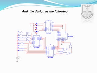
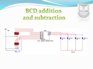
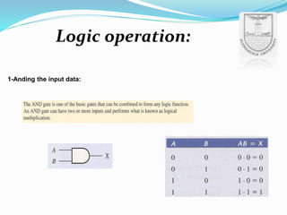


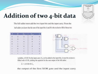
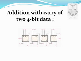
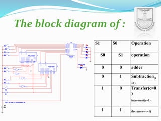
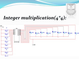
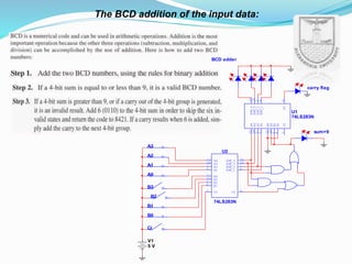
An arithmetic logic unit (ALU) is a digital circuit essential for performing arithmetic and logical operations within a computer's CPU. The concept proposed by John von Neumann in 1945 remains crucial in computer science, with ongoing research focused on enhancing ALU capabilities in modern CPUs and GPUs. The document further details various operations, block diagrams, and the functionality of ALUs, including BCD addition and different logic operations.