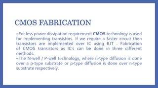
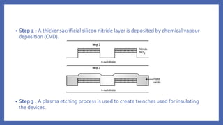
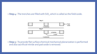
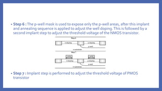
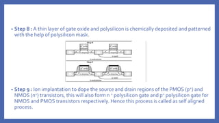
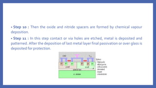
SlideShare a Scribd company logo
1 of 9
CMOS FABRICATION
USING P-WELL
VLSI DESIGN
NITHIN KALLEPALLY
CMOS FABRICATION
• For less power dissipation requirement CMOS technology is used
for implementing transistors. If we require a faster circuit then
transistors are implemented over IC using BJT . Fabrication
of CMOS transistors as IC’s can be done in three different
methods.
• The N-well / P-well technology, where n-type diffusion is done
over a p-type substrate or p-type diffusion is done over n-type
substrate respectively.
P-WELL PROCESS
• The fabrication steps of p well process are same as that of an n-well process except
that instead of n-well a p-well is implanted .The process steps involved in p-well
process are shown in Figure below.The process starts with the n type substrate
• Step 1 : A thin layer of SiO2 is deposited which will serve as the pad oxide.
• Step 2 : A thicker sacrificial silicon nitride layer is deposited by chemical vapour
deposition (CVD).
• Step 3 : A plasma etching process is used to create trenches used for insulating
the devices.
• Step 4 : The trenches are filled with SiO2 which is called as the field oxide.
• Step 5 : To provide flat surface chemical mechanical planarization is performed
and also sacrificial nitride and pad oxide is removed.
• Step 6 :The p-well mask is used to expose only the p-well areas, after this implant
and annealing sequence is applied to adjust the well doping.This is followed by a
second implant step to adjust the threshold voltage of the NMOS transistor.
• Step 7 : Implant step is performed to adjust the threshold voltage of PMOS
transistor
• Step 8 : A thin layer of gate oxide and polysilicon is chemically deposited and patterned
with the help of polysilicon mask.
• Step 9 : Ion implantation to dope the source and drain regions of the PMOS (p+) and
NMOS (n+) transistors, this will also form n + polysilicon gate and p+ polysilicon gate for
NMOS and PMOS transistors respectively. Hence this process is called as self aligned
process.
• Step 10 : Then the oxide and nitride spacers are formed by chemical vapour
deposition.
• Step 11 : In this step contact or via holes are etched, metal is deposited and
patterned. After the deposition of last metal layer final passivation or over glass is
deposited for protection.
THANK YOU…

More Related Content

What's hot (20)

Antenna PARAMETERS
Antenna PARAMETERSAntenna PARAMETERS
Antenna PARAMETERS
 
Cmos
CmosCmos
Cmos
 
Vlsi design and fabrication ppt
Vlsi design and fabrication  pptVlsi design and fabrication  ppt
Vlsi design and fabrication ppt
 
CMOS fabrication n well process
CMOS fabrication n well processCMOS fabrication n well process
CMOS fabrication n well process
 
Twin well process
Twin well processTwin well process
Twin well process
 
Cmos fabrication
Cmos fabricationCmos fabrication
Cmos fabrication
 
Short channel effects
Short channel effectsShort channel effects
Short channel effects
 
3673 mosfet
3673 mosfet3673 mosfet
3673 mosfet
 
Introduction to VLSI Design
Introduction to VLSI DesignIntroduction to VLSI Design
Introduction to VLSI Design
 
THE CMOS VLSI DESIGN
THE CMOS VLSI DESIGNTHE CMOS VLSI DESIGN
THE CMOS VLSI DESIGN
 
Short Channel Effect In MOSFET
Short Channel Effect In MOSFETShort Channel Effect In MOSFET
Short Channel Effect In MOSFET
 
Layouts
LayoutsLayouts
Layouts
 
Mosfet’s
Mosfet’sMosfet’s
Mosfet’s
 
Stick Diagram and Lambda Based Design Rules
Stick Diagram and Lambda Based Design RulesStick Diagram and Lambda Based Design Rules
Stick Diagram and Lambda Based Design Rules
 
Combinational Logic
Combinational LogicCombinational Logic
Combinational Logic
 
MOSFET fabrication 12
MOSFET fabrication 12MOSFET fabrication 12
MOSFET fabrication 12
 
Lambda design rule
Lambda design ruleLambda design rule
Lambda design rule
 
Finfets
FinfetsFinfets
Finfets
 
VLSI Design(Fabrication)
VLSI Design(Fabrication)VLSI Design(Fabrication)
VLSI Design(Fabrication)
 
Second order effects
Second order effectsSecond order effects
Second order effects
 

Similar to CMOS Fabrication using P-well -VLSI

CMOS fabrication.pptx
CMOS fabrication.pptxCMOS fabrication.pptx
CMOS fabrication.pptxtemp2424
 
3. CMOS Fabrication.ppt important to read
3. CMOS Fabrication.ppt important to read3. CMOS Fabrication.ppt important to read
3. CMOS Fabrication.ppt important to readSahithikairamkonda
 
VLSI_chapter1.pptx
VLSI_chapter1.pptxVLSI_chapter1.pptx
VLSI_chapter1.pptxroyal sethi
 
3_DVD_IC_Fabrication_Flow_designer_perspective.pdf
3_DVD_IC_Fabrication_Flow_designer_perspective.pdf3_DVD_IC_Fabrication_Flow_designer_perspective.pdf
3_DVD_IC_Fabrication_Flow_designer_perspective.pdfUsha Mehta
 
EEE 4157_Lecture_7_8_9.ppt
EEE 4157_Lecture_7_8_9.pptEEE 4157_Lecture_7_8_9.ppt
EEE 4157_Lecture_7_8_9.pptOmarFaruqe23
 
IC fabrication and its types with real life applications.pptx
IC fabrication and its types with real life applications.pptxIC fabrication and its types with real life applications.pptx
IC fabrication and its types with real life applications.pptxNishanth Asmi
 
VLSI-mosfet-construction engineering ECE
VLSI-mosfet-construction engineering ECEVLSI-mosfet-construction engineering ECE
VLSI-mosfet-construction engineering ECEjpradha86
 
Lecture 2 ic fabrication processing & wafer preparation
Lecture 2 ic fabrication processing & wafer preparationLecture 2 ic fabrication processing & wafer preparation
Lecture 2 ic fabrication processing & wafer preparationDr. Ghanshyam Singh
 
lect0-intro.ppt
lect0-intro.pptlect0-intro.ppt
lect0-intro.pptNickYu23
 

Similar to CMOS Fabrication using P-well -VLSI (20)

Lecture4 nmos process
Lecture4 nmos processLecture4 nmos process
Lecture4 nmos process
 
CMOS fabrication.pptx
CMOS fabrication.pptxCMOS fabrication.pptx
CMOS fabrication.pptx
 
N well process
N well processN well process
N well process
 
3. CMOS Fabrication.ppt important to read
3. CMOS Fabrication.ppt important to read3. CMOS Fabrication.ppt important to read
3. CMOS Fabrication.ppt important to read
 
Vlsi 2
Vlsi 2Vlsi 2
Vlsi 2
 
CMOS N-WELL.pptx
CMOS N-WELL.pptxCMOS N-WELL.pptx
CMOS N-WELL.pptx
 
Cmos
CmosCmos
Cmos
 
My VLSI.pptx
My VLSI.pptxMy VLSI.pptx
My VLSI.pptx
 
VLSI_chapter1.pptx
VLSI_chapter1.pptxVLSI_chapter1.pptx
VLSI_chapter1.pptx
 
Vlsi 1
Vlsi 1Vlsi 1
Vlsi 1
 
3_DVD_IC_Fabrication_Flow_designer_perspective.pdf
3_DVD_IC_Fabrication_Flow_designer_perspective.pdf3_DVD_IC_Fabrication_Flow_designer_perspective.pdf
3_DVD_IC_Fabrication_Flow_designer_perspective.pdf
 
EEE 4157_Lecture_7_8_9.ppt
EEE 4157_Lecture_7_8_9.pptEEE 4157_Lecture_7_8_9.ppt
EEE 4157_Lecture_7_8_9.ppt
 
IC fabrication and its types with real life applications.pptx
IC fabrication and its types with real life applications.pptxIC fabrication and its types with real life applications.pptx
IC fabrication and its types with real life applications.pptx
 
Cmos process flow
Cmos process flowCmos process flow
Cmos process flow
 
VLSI-mosfet-construction engineering ECE
VLSI-mosfet-construction engineering ECEVLSI-mosfet-construction engineering ECE
VLSI-mosfet-construction engineering ECE
 
Lecture 2 ic fabrication processing & wafer preparation
Lecture 2 ic fabrication processing & wafer preparationLecture 2 ic fabrication processing & wafer preparation
Lecture 2 ic fabrication processing & wafer preparation
 
Module-1.pptx
Module-1.pptxModule-1.pptx
Module-1.pptx
 
layout.pdf
layout.pdflayout.pdf
layout.pdf
 
Sp15 bee-112(fabrication)
Sp15 bee-112(fabrication)Sp15 bee-112(fabrication)
Sp15 bee-112(fabrication)
 
lect0-intro.ppt
lect0-intro.pptlect0-intro.ppt
lect0-intro.ppt
 

More from NITHIN KALLE PALLY

Formats for coherent optical communications -OPTICAL COMMUNICATIONS
Formats for coherent optical communications -OPTICAL COMMUNICATIONSFormats for coherent optical communications -OPTICAL COMMUNICATIONS
Formats for coherent optical communications -OPTICAL COMMUNICATIONSNITHIN KALLE PALLY
 
Based Interferometric Sensors- OPTICAL COMMUNICATION
Based Interferometric Sensors- OPTICAL COMMUNICATIONBased Interferometric Sensors- OPTICAL COMMUNICATION
Based Interferometric Sensors- OPTICAL COMMUNICATIONNITHIN KALLE PALLY
 
SHORT CHANNEL EFFECTS IN MOSFETS- VLSI DESIGN
SHORT CHANNEL EFFECTS IN MOSFETS- VLSI DESIGNSHORT CHANNEL EFFECTS IN MOSFETS- VLSI DESIGN
SHORT CHANNEL EFFECTS IN MOSFETS- VLSI DESIGNNITHIN KALLE PALLY
 
ANALYTIC SIGNAL GENERATION- DIGITAL SIGNAL PROCESSORS AND ARCHITECTURE ...
ANALYTIC SIGNAL GENERATION- DIGITAL SIGNAL PROCESSORS AND ARCHITECTURE       ...ANALYTIC SIGNAL GENERATION- DIGITAL SIGNAL PROCESSORS AND ARCHITECTURE       ...
ANALYTIC SIGNAL GENERATION- DIGITAL SIGNAL PROCESSORS AND ARCHITECTURE ...NITHIN KALLE PALLY
 
VLAN -VIRTUAL LAN -COMPUTER NETWORKS
VLAN -VIRTUAL LAN -COMPUTER NETWORKSVLAN -VIRTUAL LAN -COMPUTER NETWORKS
VLAN -VIRTUAL LAN -COMPUTER NETWORKSNITHIN KALLE PALLY
 
Gray Image Watermarking using slant transform - digital image processing
Gray Image Watermarking using slant transform - digital image processingGray Image Watermarking using slant transform - digital image processing
Gray Image Watermarking using slant transform - digital image processingNITHIN KALLE PALLY
 
RELATION BETWEEN DATA WORD SIZE AND INSTRUCTION WORD SIZE- Dspa word size
RELATION BETWEEN DATA WORD SIZE AND INSTRUCTION WORD SIZE- Dspa word sizeRELATION BETWEEN DATA WORD SIZE AND INSTRUCTION WORD SIZE- Dspa word size
RELATION BETWEEN DATA WORD SIZE AND INSTRUCTION WORD SIZE- Dspa word sizeNITHIN KALLE PALLY
 
DISTINGUISH BETWEEN WALSH TRANSFORM AND HAAR TRANSFORMDip transforms
DISTINGUISH BETWEEN WALSH TRANSFORM AND HAAR TRANSFORMDip transformsDISTINGUISH BETWEEN WALSH TRANSFORM AND HAAR TRANSFORMDip transforms
DISTINGUISH BETWEEN WALSH TRANSFORM AND HAAR TRANSFORMDip transformsNITHIN KALLE PALLY
 
Need of research and types of research
Need of research and types of researchNeed of research and types of research
Need of research and types of researchNITHIN KALLE PALLY
 
8051 architecture and pin configuration
8051 architecture and pin configuration8051 architecture and pin configuration
8051 architecture and pin configurationNITHIN KALLE PALLY
 
TRANSITIONAL BUTTERWORTH-CHEBYSHEV FILTERS
TRANSITIONALBUTTERWORTH-CHEBYSHEV FILTERSTRANSITIONALBUTTERWORTH-CHEBYSHEV FILTERS
TRANSITIONAL BUTTERWORTH-CHEBYSHEV FILTERSNITHIN KALLE PALLY
 
CAUSES AND EFFECTS OF LANDSLIDES
CAUSES AND EFFECTS OF LANDSLIDESCAUSES AND EFFECTS OF LANDSLIDES
CAUSES AND EFFECTS OF LANDSLIDESNITHIN KALLE PALLY
 
FUTURE PUBLIC LAND MOBILE TELECOMMUNICATION SYSTEMS(FPLMTS) AND INFORMA...
      FUTURE PUBLIC LAND MOBILE TELECOMMUNICATION SYSTEMS(FPLMTS) AND INFORMA...      FUTURE PUBLIC LAND MOBILE TELECOMMUNICATION SYSTEMS(FPLMTS) AND INFORMA...
FUTURE PUBLIC LAND MOBILE TELECOMMUNICATION SYSTEMS(FPLMTS) AND INFORMA...NITHIN KALLE PALLY
 
SAMPLING AND STORAGE OSCILLOSCOPE
SAMPLING AND STORAGE OSCILLOSCOPESAMPLING AND STORAGE OSCILLOSCOPE
SAMPLING AND STORAGE OSCILLOSCOPENITHIN KALLE PALLY
 

More from NITHIN KALLE PALLY (15)

Formats for coherent optical communications -OPTICAL COMMUNICATIONS
Formats for coherent optical communications -OPTICAL COMMUNICATIONSFormats for coherent optical communications -OPTICAL COMMUNICATIONS
Formats for coherent optical communications -OPTICAL COMMUNICATIONS
 
Based Interferometric Sensors- OPTICAL COMMUNICATION
Based Interferometric Sensors- OPTICAL COMMUNICATIONBased Interferometric Sensors- OPTICAL COMMUNICATION
Based Interferometric Sensors- OPTICAL COMMUNICATION
 
SHORT CHANNEL EFFECTS IN MOSFETS- VLSI DESIGN
SHORT CHANNEL EFFECTS IN MOSFETS- VLSI DESIGNSHORT CHANNEL EFFECTS IN MOSFETS- VLSI DESIGN
SHORT CHANNEL EFFECTS IN MOSFETS- VLSI DESIGN
 
ANALYTIC SIGNAL GENERATION- DIGITAL SIGNAL PROCESSORS AND ARCHITECTURE ...
ANALYTIC SIGNAL GENERATION- DIGITAL SIGNAL PROCESSORS AND ARCHITECTURE       ...ANALYTIC SIGNAL GENERATION- DIGITAL SIGNAL PROCESSORS AND ARCHITECTURE       ...
ANALYTIC SIGNAL GENERATION- DIGITAL SIGNAL PROCESSORS AND ARCHITECTURE ...
 
VLAN -VIRTUAL LAN -COMPUTER NETWORKS
VLAN -VIRTUAL LAN -COMPUTER NETWORKSVLAN -VIRTUAL LAN -COMPUTER NETWORKS
VLAN -VIRTUAL LAN -COMPUTER NETWORKS
 
Gray Image Watermarking using slant transform - digital image processing
Gray Image Watermarking using slant transform - digital image processingGray Image Watermarking using slant transform - digital image processing
Gray Image Watermarking using slant transform - digital image processing
 
web2.0 - computer networks
web2.0 - computer networksweb2.0 - computer networks
web2.0 - computer networks
 
RELATION BETWEEN DATA WORD SIZE AND INSTRUCTION WORD SIZE- Dspa word size
RELATION BETWEEN DATA WORD SIZE AND INSTRUCTION WORD SIZE- Dspa word sizeRELATION BETWEEN DATA WORD SIZE AND INSTRUCTION WORD SIZE- Dspa word size
RELATION BETWEEN DATA WORD SIZE AND INSTRUCTION WORD SIZE- Dspa word size
 
DISTINGUISH BETWEEN WALSH TRANSFORM AND HAAR TRANSFORMDip transforms
DISTINGUISH BETWEEN WALSH TRANSFORM AND HAAR TRANSFORMDip transformsDISTINGUISH BETWEEN WALSH TRANSFORM AND HAAR TRANSFORMDip transforms
DISTINGUISH BETWEEN WALSH TRANSFORM AND HAAR TRANSFORMDip transforms
 
Need of research and types of research
Need of research and types of researchNeed of research and types of research
Need of research and types of research
 
8051 architecture and pin configuration
8051 architecture and pin configuration8051 architecture and pin configuration
8051 architecture and pin configuration
 
TRANSITIONAL BUTTERWORTH-CHEBYSHEV FILTERS
TRANSITIONALBUTTERWORTH-CHEBYSHEV FILTERSTRANSITIONALBUTTERWORTH-CHEBYSHEV FILTERS
TRANSITIONAL BUTTERWORTH-CHEBYSHEV FILTERS
 
CAUSES AND EFFECTS OF LANDSLIDES
CAUSES AND EFFECTS OF LANDSLIDESCAUSES AND EFFECTS OF LANDSLIDES
CAUSES AND EFFECTS OF LANDSLIDES
 
FUTURE PUBLIC LAND MOBILE TELECOMMUNICATION SYSTEMS(FPLMTS) AND INFORMA...
      FUTURE PUBLIC LAND MOBILE TELECOMMUNICATION SYSTEMS(FPLMTS) AND INFORMA...      FUTURE PUBLIC LAND MOBILE TELECOMMUNICATION SYSTEMS(FPLMTS) AND INFORMA...
FUTURE PUBLIC LAND MOBILE TELECOMMUNICATION SYSTEMS(FPLMTS) AND INFORMA...
 
SAMPLING AND STORAGE OSCILLOSCOPE
SAMPLING AND STORAGE OSCILLOSCOPESAMPLING AND STORAGE OSCILLOSCOPE
SAMPLING AND STORAGE OSCILLOSCOPE
 

Recently uploaded

Porous Ceramics seminar and technical writing
Porous Ceramics seminar and technical writingPorous Ceramics seminar and technical writing
Porous Ceramics seminar and technical writingrakeshbaidya232001
 
VIP Call Girls Service Kondapur Hyderabad Call +91-8250192130
VIP Call Girls Service Kondapur Hyderabad Call +91-8250192130VIP Call Girls Service Kondapur Hyderabad Call +91-8250192130
VIP Call Girls Service Kondapur Hyderabad Call +91-8250192130Suhani Kapoor
 
APPLICATIONS-AC/DC DRIVES-OPERATING CHARACTERISTICS
APPLICATIONS-AC/DC DRIVES-OPERATING CHARACTERISTICSAPPLICATIONS-AC/DC DRIVES-OPERATING CHARACTERISTICS
APPLICATIONS-AC/DC DRIVES-OPERATING CHARACTERISTICSKurinjimalarL3
 
Call for Papers - African Journal of Biological Sciences, E-ISSN: 2663-2187, ...
Call for Papers - African Journal of Biological Sciences, E-ISSN: 2663-2187, ...Call for Papers - African Journal of Biological Sciences, E-ISSN: 2663-2187, ...
Call for Papers - African Journal of Biological Sciences, E-ISSN: 2663-2187, ...Christo Ananth
 
Introduction to Multiple Access Protocol.pptx
Introduction to Multiple Access Protocol.pptxIntroduction to Multiple Access Protocol.pptx
Introduction to Multiple Access Protocol.pptxupamatechverse
 
(SHREYA) Chakan Call Girls Just Call 7001035870 [ Cash on Delivery ] Pune Esc...
(SHREYA) Chakan Call Girls Just Call 7001035870 [ Cash on Delivery ] Pune Esc...(SHREYA) Chakan Call Girls Just Call 7001035870 [ Cash on Delivery ] Pune Esc...
(SHREYA) Chakan Call Girls Just Call 7001035870 [ Cash on Delivery ] Pune Esc...ranjana rawat
 
247267395-1-Symmetric-and-distributed-shared-memory-architectures-ppt (1).ppt
247267395-1-Symmetric-and-distributed-shared-memory-architectures-ppt (1).ppt247267395-1-Symmetric-and-distributed-shared-memory-architectures-ppt (1).ppt
247267395-1-Symmetric-and-distributed-shared-memory-architectures-ppt (1).pptssuser5c9d4b1
 
UNIT-V FMM.HYDRAULIC TURBINE - Construction and working
UNIT-V FMM.HYDRAULIC TURBINE - Construction and workingUNIT-V FMM.HYDRAULIC TURBINE - Construction and working
UNIT-V FMM.HYDRAULIC TURBINE - Construction and workingrknatarajan
 
(ANVI) Koregaon Park Call Girls Just Call 7001035870 [ Cash on Delivery ] Pun...
(ANVI) Koregaon Park Call Girls Just Call 7001035870 [ Cash on Delivery ] Pun...(ANVI) Koregaon Park Call Girls Just Call 7001035870 [ Cash on Delivery ] Pun...
(ANVI) Koregaon Park Call Girls Just Call 7001035870 [ Cash on Delivery ] Pun...ranjana rawat
 
College Call Girls Nashik Nehal 7001305949 Independent Escort Service Nashik
College Call Girls Nashik Nehal 7001305949 Independent Escort Service NashikCollege Call Girls Nashik Nehal 7001305949 Independent Escort Service Nashik
College Call Girls Nashik Nehal 7001305949 Independent Escort Service NashikCall Girls in Nagpur High Profile
 
Decoding Kotlin - Your guide to solving the mysterious in Kotlin.pptx
Decoding Kotlin - Your guide to solving the mysterious in Kotlin.pptxDecoding Kotlin - Your guide to solving the mysterious in Kotlin.pptx
Decoding Kotlin - Your guide to solving the mysterious in Kotlin.pptxJoão Esperancinha
 
Sheet Pile Wall Design and Construction: A Practical Guide for Civil Engineer...
Sheet Pile Wall Design and Construction: A Practical Guide for Civil Engineer...Sheet Pile Wall Design and Construction: A Practical Guide for Civil Engineer...
Sheet Pile Wall Design and Construction: A Practical Guide for Civil Engineer...Dr.Costas Sachpazis
 
HARMONY IN THE NATURE AND EXISTENCE - Unit-IV
HARMONY IN THE NATURE AND EXISTENCE - Unit-IVHARMONY IN THE NATURE AND EXISTENCE - Unit-IV
HARMONY IN THE NATURE AND EXISTENCE - Unit-IVRajaP95
 
Processing & Properties of Floor and Wall Tiles.pptx
Processing & Properties of Floor and Wall Tiles.pptxProcessing & Properties of Floor and Wall Tiles.pptx
Processing & Properties of Floor and Wall Tiles.pptxpranjaldaimarysona
 
Structural Analysis and Design of Foundations: A Comprehensive Handbook for S...
Structural Analysis and Design of Foundations: A Comprehensive Handbook for S...Structural Analysis and Design of Foundations: A Comprehensive Handbook for S...
Structural Analysis and Design of Foundations: A Comprehensive Handbook for S...Dr.Costas Sachpazis
 
(MEERA) Dapodi Call Girls Just Call 7001035870 [ Cash on Delivery ] Pune Escorts
(MEERA) Dapodi Call Girls Just Call 7001035870 [ Cash on Delivery ] Pune Escorts(MEERA) Dapodi Call Girls Just Call 7001035870 [ Cash on Delivery ] Pune Escorts
(MEERA) Dapodi Call Girls Just Call 7001035870 [ Cash on Delivery ] Pune Escortsranjana rawat
 
Microscopic Analysis of Ceramic Materials.pptx
Microscopic Analysis of Ceramic Materials.pptxMicroscopic Analysis of Ceramic Materials.pptx
Microscopic Analysis of Ceramic Materials.pptxpurnimasatapathy1234
 

Recently uploaded (20)

Porous Ceramics seminar and technical writing
Porous Ceramics seminar and technical writingPorous Ceramics seminar and technical writing
Porous Ceramics seminar and technical writing
 
VIP Call Girls Service Kondapur Hyderabad Call +91-8250192130
VIP Call Girls Service Kondapur Hyderabad Call +91-8250192130VIP Call Girls Service Kondapur Hyderabad Call +91-8250192130
VIP Call Girls Service Kondapur Hyderabad Call +91-8250192130
 
APPLICATIONS-AC/DC DRIVES-OPERATING CHARACTERISTICS
APPLICATIONS-AC/DC DRIVES-OPERATING CHARACTERISTICSAPPLICATIONS-AC/DC DRIVES-OPERATING CHARACTERISTICS
APPLICATIONS-AC/DC DRIVES-OPERATING CHARACTERISTICS
 
Call for Papers - African Journal of Biological Sciences, E-ISSN: 2663-2187, ...
Call for Papers - African Journal of Biological Sciences, E-ISSN: 2663-2187, ...Call for Papers - African Journal of Biological Sciences, E-ISSN: 2663-2187, ...
Call for Papers - African Journal of Biological Sciences, E-ISSN: 2663-2187, ...
 
Introduction to Multiple Access Protocol.pptx
Introduction to Multiple Access Protocol.pptxIntroduction to Multiple Access Protocol.pptx
Introduction to Multiple Access Protocol.pptx
 
(SHREYA) Chakan Call Girls Just Call 7001035870 [ Cash on Delivery ] Pune Esc...
(SHREYA) Chakan Call Girls Just Call 7001035870 [ Cash on Delivery ] Pune Esc...(SHREYA) Chakan Call Girls Just Call 7001035870 [ Cash on Delivery ] Pune Esc...
(SHREYA) Chakan Call Girls Just Call 7001035870 [ Cash on Delivery ] Pune Esc...
 
247267395-1-Symmetric-and-distributed-shared-memory-architectures-ppt (1).ppt
247267395-1-Symmetric-and-distributed-shared-memory-architectures-ppt (1).ppt247267395-1-Symmetric-and-distributed-shared-memory-architectures-ppt (1).ppt
247267395-1-Symmetric-and-distributed-shared-memory-architectures-ppt (1).ppt
 
UNIT-V FMM.HYDRAULIC TURBINE - Construction and working
UNIT-V FMM.HYDRAULIC TURBINE - Construction and workingUNIT-V FMM.HYDRAULIC TURBINE - Construction and working
UNIT-V FMM.HYDRAULIC TURBINE - Construction and working
 
Roadmap to Membership of RICS - Pathways and Routes
Roadmap to Membership of RICS - Pathways and RoutesRoadmap to Membership of RICS - Pathways and Routes
Roadmap to Membership of RICS - Pathways and Routes
 
(ANVI) Koregaon Park Call Girls Just Call 7001035870 [ Cash on Delivery ] Pun...
(ANVI) Koregaon Park Call Girls Just Call 7001035870 [ Cash on Delivery ] Pun...(ANVI) Koregaon Park Call Girls Just Call 7001035870 [ Cash on Delivery ] Pun...
(ANVI) Koregaon Park Call Girls Just Call 7001035870 [ Cash on Delivery ] Pun...
 
College Call Girls Nashik Nehal 7001305949 Independent Escort Service Nashik
College Call Girls Nashik Nehal 7001305949 Independent Escort Service NashikCollege Call Girls Nashik Nehal 7001305949 Independent Escort Service Nashik
College Call Girls Nashik Nehal 7001305949 Independent Escort Service Nashik
 
Decoding Kotlin - Your guide to solving the mysterious in Kotlin.pptx
Decoding Kotlin - Your guide to solving the mysterious in Kotlin.pptxDecoding Kotlin - Your guide to solving the mysterious in Kotlin.pptx
Decoding Kotlin - Your guide to solving the mysterious in Kotlin.pptx
 
Sheet Pile Wall Design and Construction: A Practical Guide for Civil Engineer...
Sheet Pile Wall Design and Construction: A Practical Guide for Civil Engineer...Sheet Pile Wall Design and Construction: A Practical Guide for Civil Engineer...
Sheet Pile Wall Design and Construction: A Practical Guide for Civil Engineer...
 
HARMONY IN THE NATURE AND EXISTENCE - Unit-IV
HARMONY IN THE NATURE AND EXISTENCE - Unit-IVHARMONY IN THE NATURE AND EXISTENCE - Unit-IV
HARMONY IN THE NATURE AND EXISTENCE - Unit-IV
 
Processing & Properties of Floor and Wall Tiles.pptx
Processing & Properties of Floor and Wall Tiles.pptxProcessing & Properties of Floor and Wall Tiles.pptx
Processing & Properties of Floor and Wall Tiles.pptx
 
Structural Analysis and Design of Foundations: A Comprehensive Handbook for S...
Structural Analysis and Design of Foundations: A Comprehensive Handbook for S...Structural Analysis and Design of Foundations: A Comprehensive Handbook for S...
Structural Analysis and Design of Foundations: A Comprehensive Handbook for S...
 
Call Us -/9953056974- Call Girls In Vikaspuri-/- Delhi NCR
Call Us -/9953056974- Call Girls In Vikaspuri-/- Delhi NCRCall Us -/9953056974- Call Girls In Vikaspuri-/- Delhi NCR
Call Us -/9953056974- Call Girls In Vikaspuri-/- Delhi NCR
 
(MEERA) Dapodi Call Girls Just Call 7001035870 [ Cash on Delivery ] Pune Escorts
(MEERA) Dapodi Call Girls Just Call 7001035870 [ Cash on Delivery ] Pune Escorts(MEERA) Dapodi Call Girls Just Call 7001035870 [ Cash on Delivery ] Pune Escorts
(MEERA) Dapodi Call Girls Just Call 7001035870 [ Cash on Delivery ] Pune Escorts
 
Microscopic Analysis of Ceramic Materials.pptx
Microscopic Analysis of Ceramic Materials.pptxMicroscopic Analysis of Ceramic Materials.pptx
Microscopic Analysis of Ceramic Materials.pptx
 
DJARUM4D - SLOT GACOR ONLINE | SLOT DEMO ONLINE
DJARUM4D - SLOT GACOR ONLINE | SLOT DEMO ONLINEDJARUM4D - SLOT GACOR ONLINE | SLOT DEMO ONLINE
DJARUM4D - SLOT GACOR ONLINE | SLOT DEMO ONLINE
 

CMOS Fabrication using P-well -VLSI

  • 1. CMOS FABRICATION USING P-WELL VLSI DESIGN NITHIN KALLEPALLY
  • 2. CMOS FABRICATION • For less power dissipation requirement CMOS technology is used for implementing transistors. If we require a faster circuit then transistors are implemented over IC using BJT . Fabrication of CMOS transistors as IC’s can be done in three different methods. • The N-well / P-well technology, where n-type diffusion is done over a p-type substrate or p-type diffusion is done over n-type substrate respectively.
  • 3. P-WELL PROCESS • The fabrication steps of p well process are same as that of an n-well process except that instead of n-well a p-well is implanted .The process steps involved in p-well process are shown in Figure below.The process starts with the n type substrate • Step 1 : A thin layer of SiO2 is deposited which will serve as the pad oxide.
  • 4. • Step 2 : A thicker sacrificial silicon nitride layer is deposited by chemical vapour deposition (CVD). • Step 3 : A plasma etching process is used to create trenches used for insulating the devices.
  • 5. • Step 4 : The trenches are filled with SiO2 which is called as the field oxide. • Step 5 : To provide flat surface chemical mechanical planarization is performed and also sacrificial nitride and pad oxide is removed.
  • 6. • Step 6 :The p-well mask is used to expose only the p-well areas, after this implant and annealing sequence is applied to adjust the well doping.This is followed by a second implant step to adjust the threshold voltage of the NMOS transistor. • Step 7 : Implant step is performed to adjust the threshold voltage of PMOS transistor
  • 7. • Step 8 : A thin layer of gate oxide and polysilicon is chemically deposited and patterned with the help of polysilicon mask. • Step 9 : Ion implantation to dope the source and drain regions of the PMOS (p+) and NMOS (n+) transistors, this will also form n + polysilicon gate and p+ polysilicon gate for NMOS and PMOS transistors respectively. Hence this process is called as self aligned process.
  • 8. • Step 10 : Then the oxide and nitride spacers are formed by chemical vapour deposition. • Step 11 : In this step contact or via holes are etched, metal is deposited and patterned. After the deposition of last metal layer final passivation or over glass is deposited for protection.