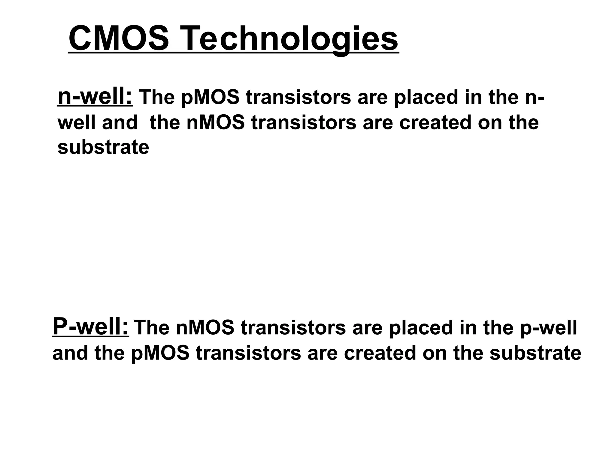
27/12/2008
VLSI Design
VLSI Design
UNIT I : Introduction to IC Technology
CMOS Inverter in n-well process
Out Line
• CMOS Inverter in n-well process
• CMOS Inverter in Twin-Tub Process
CMOS Technologies
n-well: The pMOS transistors are placed in the n-
well and the nMOS transistors are created on the
substrate
P-well: The nMOS transistors are placed in the p-well
and the pMOS transistors are created on the substrate
1.Wafer
A bare Si wafer is chosen
The type will be n or p depending upon the technology
2.Oxidation of Wafer
The wafer is oxidised at a high temperature
This must be patterned to define the n-well
3.PhotoResist deposition
•The photoresist is deposited throughout the wafer
•The PR has to be patterned to allow formation of
the well
4.n-well Mask
•The PhotoResist is exposed through the n-well mask
•The softened PhotoResist is is removed to expose
the oxide
5.Oxide Etch
•The oxide is etched with HF acid where unprotected by
PhotoResist
•The wafer is now exposed to the n-well area
6.PhotoResist removal
•The remaining PR is removed via piranha etch
•The well is ready to be formed
7.n-well Formation
The diffusion process can make the the n-well
Ion implantation can also form the same
8.Oxide Removal
The remaining oxide is stripped with HF acid
This leaves the exposed wafer with the n-well formed
9.Gate Formation
The gates are made up of polysilicon over thinox
CVD is used to grow the poly (heavily doped) layer
10.Poly Patterning
The wafer is now patterned with PhotoResist and the poly mask
Finally this leaves the device gates
11.Diffusion Pattern
Again, a protective oxide is grown and PhotoResist
deposited
PhotoResist is patterned according to the diffusion
mask
12.Wafer Exposure for Diffusion
The protective oxide is etched away
The wafer is exposed for S/D formation
13.n-Diffusion Regions
The n+ diffusion regions are formed
Polysilicon blocks the channel area
14.Self-Aligned Process
This is a self-aligned process
S/D are automatically formed adjacent to the gate
15.p-Diffusion
The p-diffusion mask is used next
This completes creation of all active regions
16.Field Oxide
The field oxide is grown to insulate wafer and metal
It is patterned with the contact mask
17.Metal Formation
•Al is sputtered over the entire area filling contact cuts too
•Metal is patterned with the metal mask
Inverter Cross-section
•Typically use p-type substrate for nMOS transistors
• Requires n-well for body of pMOS transistors
Well and Substrate Taps
Substrate must be tied to GND, n-well to VDD
 Use heavily doped well and substrate contacts / taps
Six masks
– n-well
– Polysilicon
– n+ diffusion
– p+ diffusion
– Contact
– Metal
CMOS Inverter in Twin-Tub Process
Twin Tub Processes
• Twin-tub CMOS technology provides the
basis for separate optimization of the p-
type and n-type transistors.
• One can optimize independently for
threshold voltage, body effect, and the
gain associated with n- and p-devices.
Twin Tub Process: N-well / P-well
First place wells to provide properly-doped
substrate for n-type, p-type transistors:
Twin Tub Process: Polysilicon
Pattern polysilicon before diffusion regions:
Twin Tub Process: N+/ P+ Diffusion
Add diffusions, performing self-masking:
Start adding metal layers:
Twin Tub Process: Contact / Via / Metal
Twin-well CMOS process cross section
Twin Tub CMOS Process Cross Section
---Struggle gives Strength and Dignity....

CMOS-nWELL-and-TwintnntbgTub-Process.ppt