Downloaded 11 times
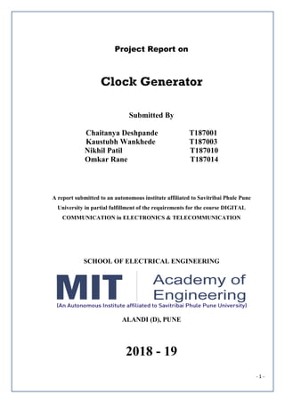
![- 5 -
2.Block Diagram and Circuit Diagram
2.1 Block Diagram
Fig 2.2 Block diagram [1]
1) Input:
In Our circuit we have input to system is nothing but battery of 9 volts.
2) Timer IC:
The 555 timer IC is an integrated circuit used in a variety of timer, pulse generation,
and oscillator applications. The 555 can be used to provide time delays, as an
oscillator, and as a flip-flop element. Derivatives provide two or four timing circuits
in one package.
3) Potentiometer:
It is variable resistor connected between pin 7 and 2 of IC pins 555. It is connected
in voltage divider configuration. Varying potentiometer resistance changes output
frequency of clock signal.
4) Output (square Wave):
As output is square wave can be observed on Digital Storage Oscilloscope or Crystal
Oscilloscope.](https://image.slidesharecdn.com/dc-190503194034/85/Clock-Generator-5-320.jpg)
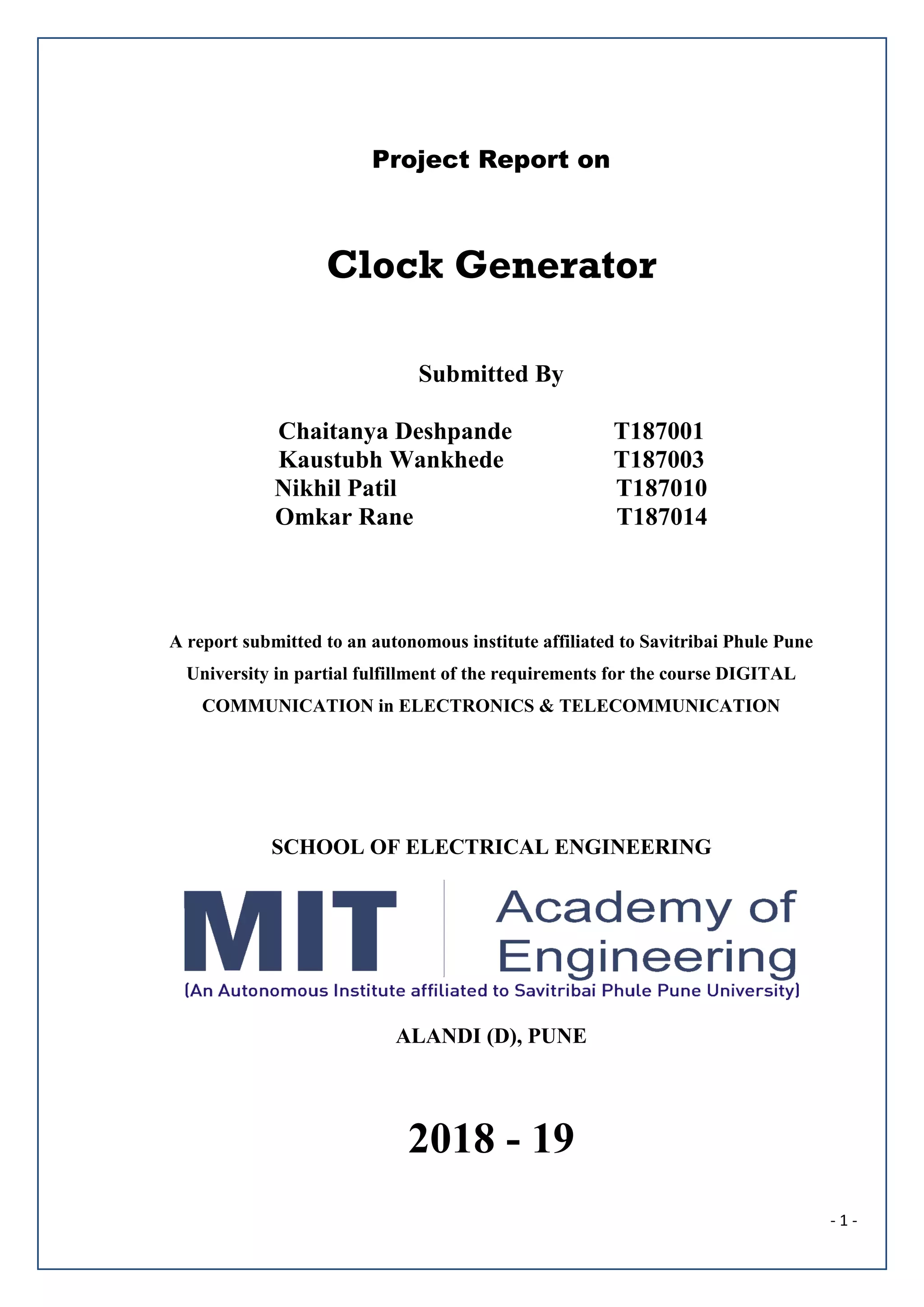
![- 6 -
2.1 Circuit Diagram
Fig 2.1 Schematic [2]
Fig 2.1 Circuit diagram [3]](https://image.slidesharecdn.com/dc-190503194034/85/Clock-Generator-6-320.jpg)
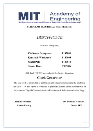
![- 7 -
Fig 2.2 PCB Layout [4]](https://image.slidesharecdn.com/dc-190503194034/85/Clock-Generator-7-320.jpg)
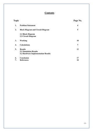
![- 8 -
PIN Description of IC 555:
Fig 2.2 Circuit diagram [4]
1) 555 supply (pins 1 and 8)
The 555 timer can be used with a supply voltage (Vs) in the range 4.5V to 15V
(18V is the absolute maximum)
Pin1 connects to 0V.
Pin 8 connects to the positive supply +Vs.
2) 555 trigger input (pin 2)
When less than 1/3 Vs ('active low') this makes the output high (+Vs). It has a high input
impedance of at least 2M . It monitors the discharging of the timing capacitor in an astable
circuit.
3) 555 threshold input (pin 6)
When greater than 2/3 Vs ('active high') this makes the output low (0V)*. It has a high input
impedance of about 10M . It monitors the charging of the timing capacitor in astable and
monostable circuits.
4) 555 reset input (pin 4)
When less than about 0.7V this makes the output low (0V), overriding the other inputs. When
not required it should be connected to +Vs.
5) 555 control input (pin 5)
This can be used to adjust the threshold voltage which is set internally to be 2/3 Vs. Usually
this function is not required and the control input is often left unconnected. If electrical noise](https://image.slidesharecdn.com/dc-190503194034/85/Clock-Generator-8-320.jpg)
![- 18 -
7.References
[1] Variable Frequency Oscillator[website]
Available: http://www.circuitstoday.com/variable-frequency-oscillator
[2] NE555 Texas Instrument Datasheet of IC 555[Online]
[4] 555 Timer Pinout [website]
Available: http://www.learningaboutelectronics.com/Articles/555-timer-pinout.php
[5] IC555 block diagram[website]
Available:chttp://www.circuitstoday.com/wp-content/uploads/2009/09/555-Timer-IC.jpg](https://image.slidesharecdn.com/dc-190503194034/85/Clock-Generator-18-320.jpg)

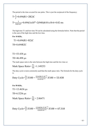
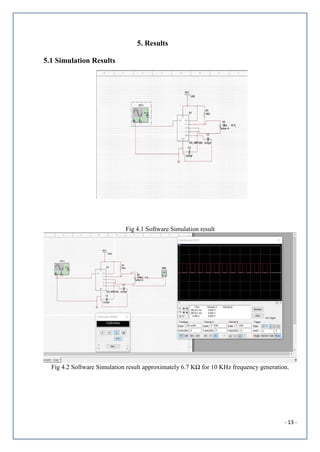
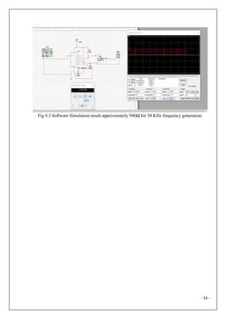
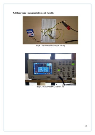
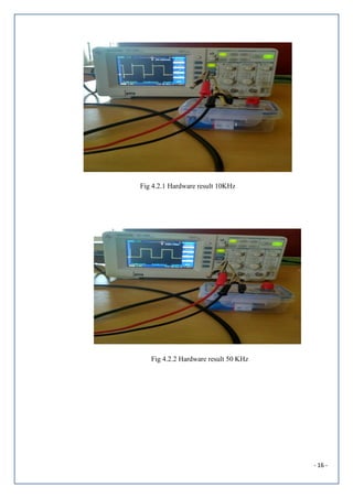
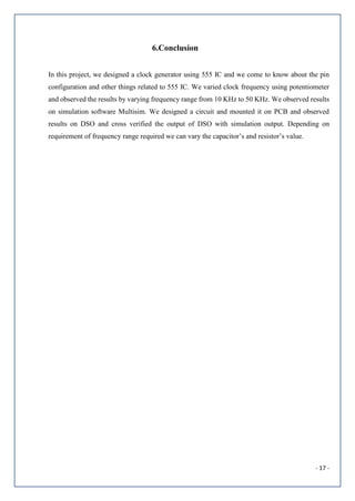
This document is a project report submitted by four students on the design of a clock generator circuit using a 555 timer IC. The circuit uses a potentiometer to vary the clock frequency from 10 kHz to 50 kHz. The report includes the block diagram, circuit diagram, calculations for determining frequency and duty cycle, simulation results from Multisim, and hardware test results from a breadboard prototype and oscilloscope measurements. The project involved designing, simulating, building and testing a clock generator circuit that successfully produces a variable frequency clock signal as required.