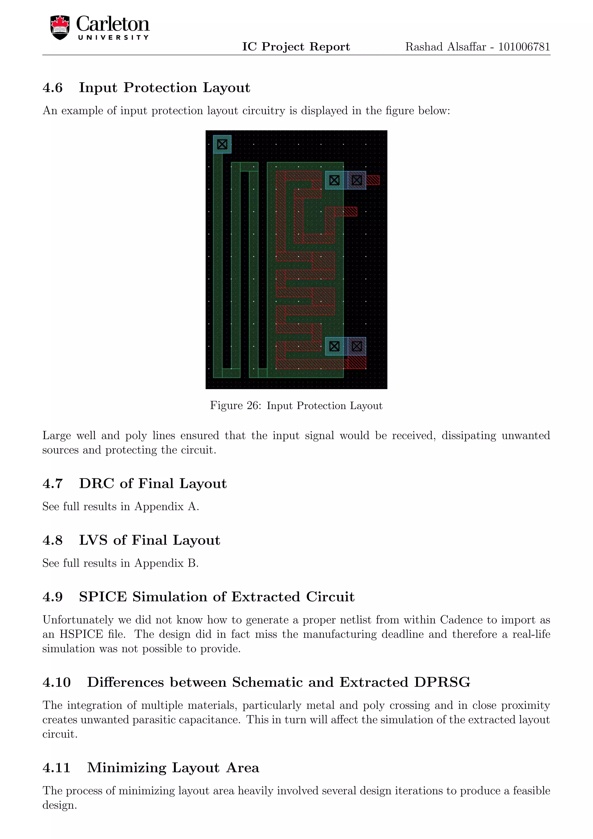
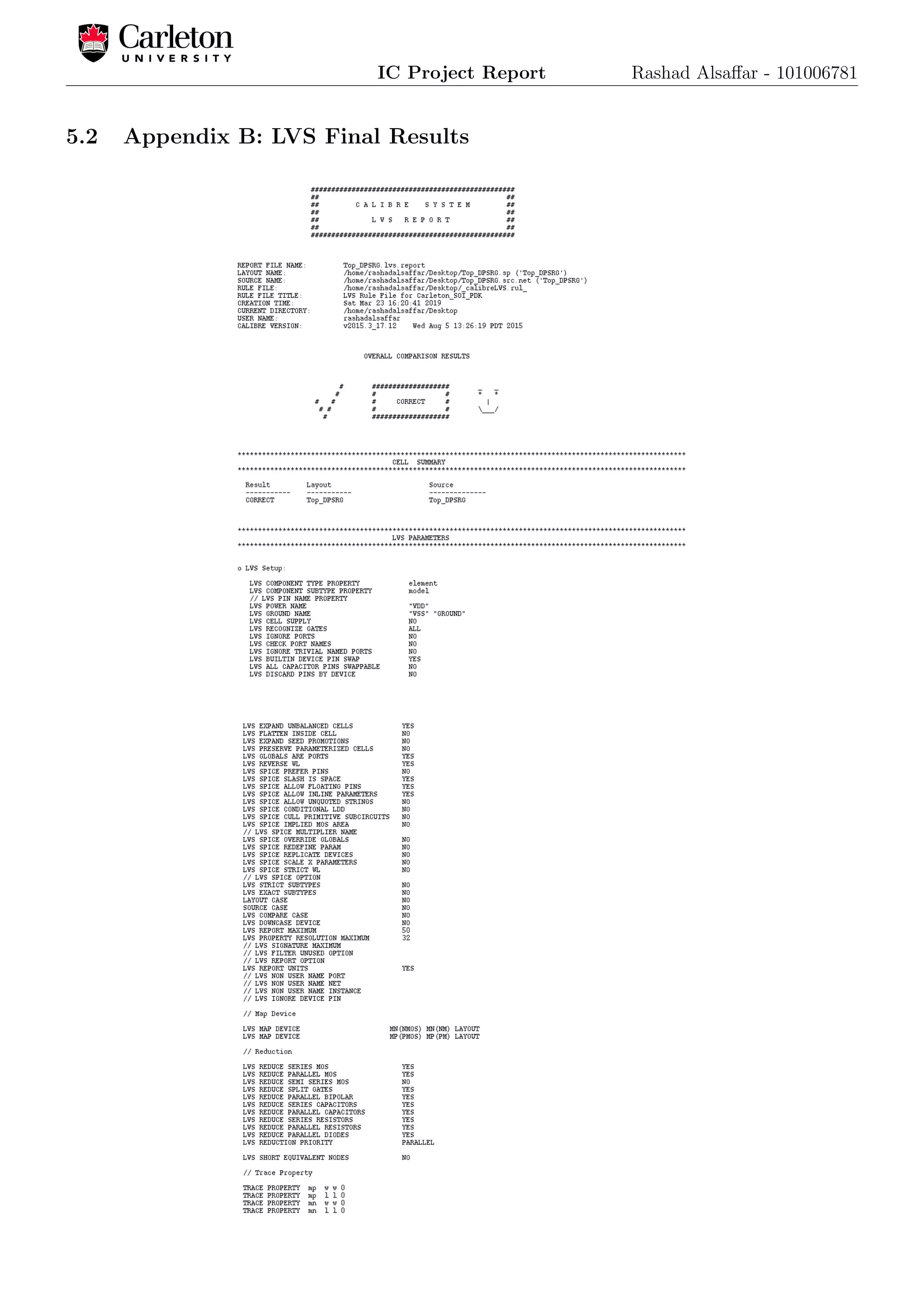
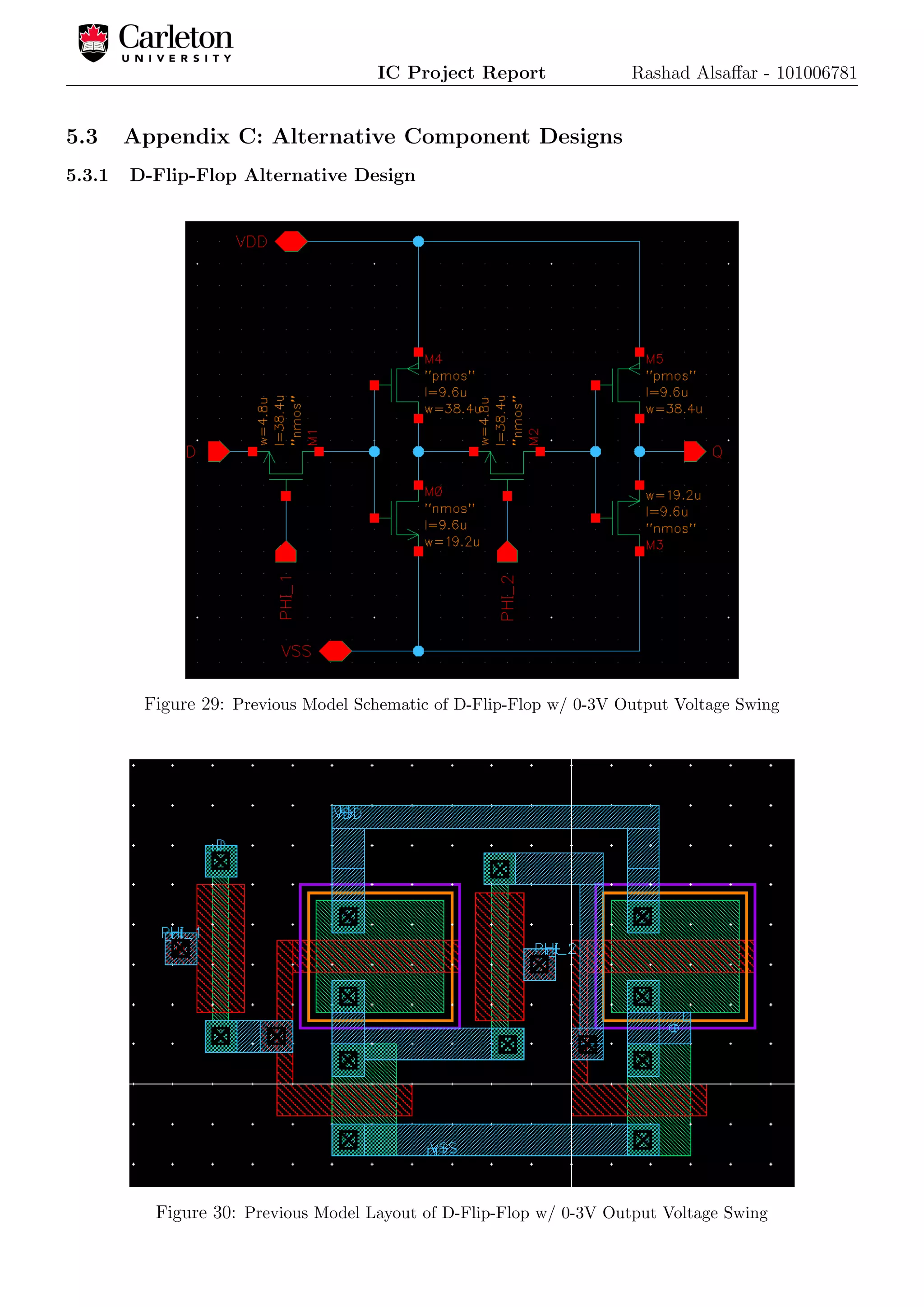
Three-phase ac motors have been the workhorse of industry since the earliest days of electrical engineering. They are reliable, efficient, cost-effective and need little or no maintenance. In addition, ac motors such as induction and reluctance motors need no electrical connection to the rotor, so can easily be made flameproof for use in hazardous environments such as in mines.
In order to provide proper speed control of an ac motor, it is necessary to supply the motor with a three phase supply of which both the voltage and the frequency can be varied. Such a supply will create a variable speed rotating field in the stator that will allow the rotor to rotate at the required speed with low slip. This ac motor drive can efficiently provide full torque from zero speed to full speed, can overspeed if necessary, and can, by changing phase rotation, easily provide bi-directional operation of the motor. A drive with these characteristics is known as a PWM (Pulse Width Modulated) motor drive.
Drives and motors are an integral part of industrial equipment from packaging,robotics, computer numerical control (CNC), machine tools, industrial pumps,and fans. Designing next-generation drive systems to lower operating costs requires complex control algorithms at very low latencies as well as a flexibleplatform to support changing needs and the ability to design multiple-axis systems.
Traditional drive systems based on ASICs, digital signal processors (DSPs), and microcontroller units lack the performance and flexibility to address these needs. Altera’s family of FPGAs provides a scalable platform that can be used to offload control algorithm elements in hardware. You may also integrate the whole drive system with industry-proven processor architectures while supporting multipletypes of encoders and industrial Ethernet protocols. This “drive on a chip” system reduces cost and simplifies development.
This document discusses various designs for digital multipliers. It begins by reviewing the basic building blocks used in digital circuits and how binary multiplication works by adding partial products. It then describes approaches for implementing multiplication, including right shift and add serial multipliers and faster parallel array and tree multipliers. Booth encoding is introduced as a technique to reduce the number of stages in a multiplier. Implementation details are provided for array and Wallace tree multipliers, including the use of compression cells like the (4,2) counter. Optimization goals for multipliers differ from adders in emphasizing reducing the critical path.
Field Programmable Gate Arrays (FPGAs) are semiconductor devices that contain programmable logic components and programmable interconnects. FPGAs can be reprogrammed to desired functionality requirements after manufacturing. The document discusses the building blocks of FPGAs, including configurable logic blocks (CLBs), interconnects, input/output blocks, block RAM, digital signal processing slices, and clock management resources. It also covers FPGA routing architectures and common FPGA design flows.
Automatic Test Pattern Generation (Testing of VLSI Design)Usha Mehta
The document discusses various methods for automatic test pattern generation (ATPG) in testing VLSI circuits, including:
1) Exhaustive and pseudo-exhaustive methods that test all possible patterns but are infeasible for large circuits.
2) Random and weighted random methods that provide confidence in detecting faults but quality depends on the circuit.
3) Deterministic methods like Boolean difference that compute test vectors to detect specific faults more efficiently than examining all vectors.
4) ATPG uses a two-phase approach - random pattern generation and fault simulation initially to detect many faults easily, followed by targeted deterministic pattern generation to detect remaining faults.
This document discusses pipelining as an approach to optimize sequential circuits. It describes how pipelining can be implemented using registers between logic blocks to improve resource utilization and increase throughput. This allows computations to be spread over multiple clock cycles in an assembly-line fashion. The document also discusses latch-based vs register-based pipelines and different logic styles like NORA-CMOS that can be used for pipelined structures. It covers design rules and considerations for ensuring correct pipelined operation. Finally, it briefly describes non-bistable sequential circuits like astable, monostable and Schmitt trigger circuits.
This document discusses integrated circuits (ICs) and their manufacturing. It describes how ICs are miniature circuits on semiconductor chips that contain components like transistors and diodes. The two main techniques for manufacturing ICs are the bipolar technique and metal oxide semiconductor (MOS) technique. It also discusses different categories of digital ICs based on their scale of integration, including small-scale, medium-scale, large-scale, and very-large scale integration circuits. Factors that influence IC technology choices are also summarized.
This document provides an introduction and overview of flip flops and RS latches. It defines a flip flop as a circuit that has two stable states and can store state information. It describes the main types of flip flops as asynchronous and synchronous, and lists some examples like the RS latch and JK flip flop. It then explains the key differences between asynchronous and synchronous circuits. The document proceeds to describe the RS latch in more detail, including providing its block diagram, logical diagram using NAND gates, truth table, and descriptions of its inputs, outputs, operation, and states.
The document describes the Xilinx 4000 series FPGA. It consists of configurable logic blocks (CLBs) connected through a programmable interconnect structure. Each CLB contains logic elements, flip flops, and configurable function generators. The interconnect structure includes direct connections between neighboring CLBs as well as general routing resources. Input/output blocks around the perimeter provide external connectivity. FPGAs offer advantages like rapid design times, flexibility for updates, and lower costs compared to ASICs, though ASICs can provide higher performance.
The document discusses binary multipliers. It describes how a combinational multiplier circuit performs multiplication by multiplying the multiplicand by each bit of the multiplier starting from the least significant bit. Each multiplication forms a partial product that is shifted left. The final product is the sum of the partial products. It then provides examples of 2-bit by 2-bit and 4-bit by 3-bit binary multipliers, showing how the partial products are generated using AND gates and added using half adders or full adders.
This document is the main project report for a 2D robotic plotter (CNC model) created by four students at the Government Engineering College Idukki. It describes the hardware and software used to build a 2D robotic plotter controlled by an Arduino microcontroller. The plotter uses stepper motors for the X and Y axes and a servo motor to control the pen. Software like Inkscape, CAMotics, Arduino IDE and Processing were used to design drawings, generate gcode files, and program the Arduino. The report provides details of the various components, software programs, and overall design and functioning of the 2D robotic plotter built as part of fulfilling B.Tech degree requirements.
This document discusses various low power techniques for integrated circuits. It begins by describing the increasing challenges of power consumption as device densities and clock frequencies increase while supply voltages and threshold voltages decrease. It then discusses different types of power consumption, including dynamic power, static power, leakage power from different sources, and how they can be reduced. The document covers many low power design techniques like multi-threshold CMOS, clock gating, multi-voltage, DVFS, and more. It discusses the evolution of these techniques and challenges in their implementation like timing issues, level shifters, and floorplanning for multi-voltage designs.
This document discusses several methods for designing sequential circuits, including state table reduction, state assignment, derivation of flip-flop input equations, and realization using logic gates. It provides an example of designing a comparator circuit using an iterative approach with identical cells. The document also describes implementing sequential circuits using ROMs, PLAs, CPLDs and FPGAs, giving examples of a code converter and parallel adder circuit designs for each method.
The document discusses sensors and transducers. It defines a transducer as a device that converts one form of energy to another, with sensors detecting signals from the real world and actuators generating signals. Electronic sensors typically use primary transducers to convert a parameter into an electrical signal, and secondary transducers to further process the signal. Common sensor components and configurations are described such as op-amps, instrumentation amplifiers, and connecting sensors to microcontrollers and networks. The document also covers transducer types including mechanical, thermal, optical, and chemical. Sensor calibration techniques are discussed to address non-ideal sensor effects.
This document discusses Wallace tree multiplication. It begins by explaining the basic concept of a Wallace tree multiplier using 1-bit full adders to compress the number of bits at each stage. It then provides examples of 6x6 multipliers using Wallace trees. It notes that a 32-bit multiplier using this method would have 9 adder delays. Finally, it asks questions about extending this to a 64-bit multiplier and whether other compression schemes could reduce the delay further.
2019 2 testing and verification of vlsi design_verificationUsha Mehta
This document provides an introduction to verification of VLSI designs and functional verification. It discusses sources of errors in specifications and implementations, ways to reduce human errors through automation and mistake-proofing techniques. It also covers the reconvergence model of verification, different verification methods like simulation, formal verification and techniques like equivalence checking and model checking. The document then discusses verification flows, test benches, different types of test cases and limitations of functional verification.
Hardware description languages (HDLs) allow designers to describe digital systems at different levels of abstraction in a textual format. The two most commonly used HDLs are Verilog and VHDL. Verilog is commonly used in the US, while VHDL is more popular in Europe. HDLs enable simulation of designs before fabrication to verify functionality. Digital designs can be modeled at the gate level, data flow level, or behavioral level in Verilog. Verilog code consists of a design module and test bench module to stimulate inputs and observe outputs.
This document describes the design of a Wallace tree multiplier using Verilog. It discusses different types of multipliers such as array, serial/parallel, and Booth multipliers. It provides details on the Wallace tree multiplier design including its block diagram, partitioning of partial products, number of levels, submodules like AND gates and full adders, and comparison of its power consumption and results. The dumping process in an FPGA kit is also covered along with the advantage of small delay and disadvantage of complex layout for the Wallace tree multiplier.
The PIC 16F877A microcontroller uses a Harvard architecture with separate program and data buses. It has 8kB of flash memory, 368 bytes of RAM, and 256 bytes of EEPROM. It features five I/O ports, three timers, USART serial communication, and 15 interrupt sources. Instructions are in RISC format and execute in 4 machine cycles, with most instructions completing in one cycle.
This document provides an overview of using Verilog and Xilinx Vivado to design and simulate a simple combinational circuit. It describes setting up Vivado, writing Verilog code for a full adder circuit, synthesizing the code, writing a testbench, running a simulation, and verifying the results in the waveform. The goal is to familiarize users with the typical workflow of a computer-aided design tool for digital circuits.
Fault Simulation (Testing of VLSI Design)Usha Mehta
This document provides an overview of fault simulation for testing VLSI designs. It discusses:
- The major steps of fault simulation including generating random patterns, simulating the fault-free circuit output, inserting faults, and simulating the faulty circuit output.
- Types of circuit simulators including event-driven, cycle-based, and compiled code simulators.
- Techniques for gate evaluation in simulators like truth tables, input scanning, and input counting.
- The goals of fault simulation as measuring test pattern effectiveness, guiding test pattern generation, and generating fault dictionaries.
The document discusses the career prospects for graduating engineers in India's VLSI industry. It notes the growing demand for skilled VLSI engineers and the talent shortage India faces. It highlights the knowledge and skills gap in fresh graduates, including lack of VLSI design skills, problem solving, and soft skills. The document proposes that a holistic VLSI training program encompassing all key skills could help alleviate the talent crunch by making freshers job-ready for India's booming semiconductor industry.
- ARM was developed in 1983 by Acorn Computers with a 4-man team to replace the 6502 processor in BBC computers. It has since become one of the most widely used processor cores in the world due to its simplicity, low power consumption, and use in portable devices.
- ARM Holdings licenses the ARM processor core designs to manufacturers but does not manufacture the chips itself. ARM cores power many products including PDAs, phones, media players, handheld game consoles, digital cameras, and more. Popular ARM architectures include ARM7TDMI and ARM9TDMI.
- The ARM architecture uses a load/store design with 32-bit fixed-length instructions operating on a large number of general purpose
13. peripheral component interconnect (pci)Rumah Belajar
Peripheral Component Interconnect (PCI) is a computer expansion bus standard that allows additional cards to be added to a computer motherboard. It uses a dual independent bus (DIB) architecture with a frontside bus and backside bus. PCI operates at speeds between 33-133 MHz and uses a 32-bit or 64-bit wide data path. Newer versions of PCI such as PCI-X and PCI Express have increased speeds and bandwidth capabilities.
This document presents a project book on designing DCMPL logic circuits in a 28nm process technology. It was authored by Itamar Greenberg and Shay Rubinstein from the Department of Electrical Engineering at Bar Ilan University. The document includes an introduction to CMOS scaling challenges, a literature survey of logic families such as diode logic, RTL, TTL, NMOS, PMOS and CMOS. It describes the design, modeling, layout and simulation of various digital logic gates including NOR3, NOR4, OR3 and OR4 gates. Simulation results on propagation delay, energy consumption, voltage transfer curves and noise margins are presented and analyzed.
This project is concerned with the
design of SoC for detecting and correcting the error which may occur in the memory unit due to
radiation in LEO (Lower Earth Orbit) and due to stuck-at faults in memory unit in space station.
The error free data is feed to the predestined processor using the serial communication protocol
(UART) and perform its function specified in the data input which is sent from the ground station.
A typical design flow follows the below structure and can be broken down into multiple steps. Some of these phases happen in parallel and some in sequentially.
Requirements
A customer of a semiconductor firm is typically some other company who plans to use the chip in its systems or end products. So, the customer's requirements also play an important role in deciding how the chip should be designed.
The first step is to collect the requirements, estimate the end product's market value, and evaluate the number of resources required to do the project.
Specifications
The next step is to collect specifications that describe the functionality, interface abstractly, and over all architecture of the chip to be designed. This can be something along the lines such as:
Play
Next
Unmute
Current TimeÂ
0:00
/
DurationÂ
18:10
Â
Fullscreen
Backward Skip 10s
Play Video
Forward Skip 10s
Requires computational power to run imaging algorithms to support virtual reality.
Requires two ARM A53 processors with coherent interconnect and should run at 600 MHz.
Requires USB 3.0, Bluetooth, and PCIe 2nd gen interfaces.
It should support 1920x1080 pixel displays with an appropriate controller.
Digital Design
Because of the complex nature of modern chips, it's impossible to build something from scratch, and in many cases, many components will be reused.
For example, company A requires a FlexCAN module to interact with other modules in an automobile. They can either buy the FlexCAN design from another company to save time and effort or spend resources to build one.
It's not practical to design such a system from basic building blocks such as flip-flops and CMOS transistors.
Instead, a behavioral description is developed to analyze the design in terms of functionality, performance, and other high-level issues using a Hardware Description Language such as Verilog or VHDL.
This is usually done by a digital designer and is similar to a high-level computer programmer equipped with digital electronics skills.
Verification
Once the RTL design is ready, it needs to be verified for functional correctness.
For example, a DSP processor is expected to issue bus transactions with fetching instructions from memory and know that this will happen as expected.
The functional verification is required at this point, which is done with EDA simulators' help that can model the design and apply a different stimulus to it. This is the job of a pre-silicon verification engineer.
Logic Synthesis
Now we will convert this design into hardware schematic with real elements such as combinational gates and flip-flops. This step is called synthesis.
Logic synthesis tools enable the conversion of RTL description in HDL to a gate-level netlist. This netlist is a description of the circuit in terms of gates and connections between them.
Logic synthesis tools ensure that the netlist meets timing, area, and power specifications. Typically, they have access to different technology node
Designed a microwave amplifier circuit with a required bandwidth of 250MHz at a center frequency of 3.7GHz experiencing 6.5dB gain within Keysight ADS.
This document describes the design and implementation of a high voltage, high resolution digital-to-analog converter (DAC) for driving deformable mirrors. The design uses a floating DAC architecture with a high voltage DAC providing the ground reference for a secondary low voltage, high resolution DAC. This allows the system to achieve the high voltage range of the primary DAC while maintaining the high resolution of the secondary DAC. The document details the component selection, circuit designs for single channel and multi-channel boards, and test results demonstrating a resolution of 1.6mV over a 60V range.
This document is a project report submitted by four students for their Bachelor of Engineering degree. It describes the development of a microcontroller-based interactive voice response system. The system uses a microcontroller and other ICs interfaced to a PC to allow telephone users to access information from a database by following voice prompts. The report includes details of the hardware and software design, component selection, circuit diagrams, programming code and testing procedures. It aims to provide a low-cost alternative to commercial IVR systems for small businesses.
This document is a project report that describes the design and implementation of a microcontroller-based password protected home appliance. The system uses an ATmega8 microcontroller to control a keypad, LCD display, buzzer, and relay. When the correct four-digit password is entered on the keypad, the relay activates to power the appliance and a message is displayed on the LCD. If an incorrect password is entered, the buzzer sounds and access is denied. The report provides details on the hardware components, software code, and circuit diagrams.
This thesis seeks to improve communication between a host computer and onboard peripherals of an existing low-cost robot used for teaching autonomous systems at University of Innsbruck. Several prototypes were evaluated to find the best solution, including a microcontroller board and single-board computers. The final solution uses an ATmega32 microcontroller programmed to read data from an Android phone and control the robot. Firmware was written for the microcontroller along with an Android application. This improved the robot's modularity and provides easy-to-use interfaces for students.
This document describes a top-down digital design flow using Synopsys Design Compiler for logic synthesis, Mentor Modelsim for simulation, and Cadence Encounter for placement and routing. It provides details on each step of the flow, from RTL design and simulation to logic synthesis, placement and routing, and back-annotation. An example FIR filter design is used to demonstrate the full flow. Guidelines are given for organizing design projects and files using scripts to automate the flow.
This document describes a top-down digital design flow using Synopsys Design Compiler for logic synthesis, Mentor Modelsim for simulation, and Cadence Encounter for placement and routing. It provides instructions for each step of the flow, from RTL design and simulation to synthesis, placement and routing, and back-annotation. An example FIR filter design is used to demonstrate the full flow. The document also recommends organizing design projects using a script that sets up a directory structure to manage design files for the different EDA tools.
Cd00004444 understanding-and-minimising-adc-conversion-errors-stmicroelectronicsvu CAO
The document discusses understanding and minimizing errors in analog to digital conversion. It explains that the ADC converts analog signals to digital values but is subject to various errors from factors like noise, voltage sources, and PCB layout. It provides techniques to minimize errors, such as reducing noise, improving voltage regulation, and carefully designing PCB layout and analog signal paths.
A High Speed Successive Approximation Pipelined ADC.pdfKathryn Patel
This document is a thesis submitted by Pushpak Dagade for the degree of Master of Technology in Integrated Electronics & Circuits at the Indian Institute of Technology, Delhi, under the guidance of Prof. G. S. Visweswaran. The thesis presents the design of a high-speed successive approximation pipelined (SAP) analog-to-digital converter (ADC). Chapter 1 introduces successive approximation algorithms and different types of successive approximation ADCs. The aim of the project is to design an 8-bit SAP ADC and demonstrate its potential for high-speed conversion applications.
This document describes a student project to design and implement a prototype aviation control unit using LabVIEW software and hardware interfaces. The project aims to replicate key functions of a real aviation control unit such as detecting aircraft with an IR sensor, communicating between the control unit and pilot, and controlling runway lights. The students implemented systems for aircraft detection, motor control, data logging, user login, and a flight schedule announcement board. Some issues encountered included limitations of the breadboard setup and slow performance from multiple while loops updating data constantly. Overall the prototype was able to perform all functions as planned without difficulties.
Find out more about Infineon on our Homepage: www.infineon.com
The BCR401U is a cost efficient LED driver from Infineon to drive low power LEDs. You want to know more about advantages, applications details and features of BCR401U? This publication aims to provide an overview of the LED Driver "BCR401U".
A High Speed Successive Approximation Pipelined ADCPushpak Dagade
This document describes a thesis submitted by Pushpak Dagade for the degree of Master of Technology in Integrated Electronics & Circuits. The thesis proposes a new successive approximation pipelined (SAP) ADC architecture to overcome speed limitations of traditional SAR ADCs. It presents the design of a 8-bit SAP ADC including components like a D flip-flop, comparator, and DAC. Simulation results demonstrating the SAP ADC's operation are also included. The thesis concludes with proposals for further work on the schematic, layout, and post-fabrication testing.
The document is a datasheet for the BCR402U LED driver from Infineon Technologies. It provides specifications, electrical characteristics, and application information for the device. The BCR402U is a cost-efficient LED driver that can deliver up to 65mA of output current. It has features like constant current regulation, adjustable output via an external resistor, supply voltage operation up to 40V, and a negative temperature coefficient for reduced output at higher temperatures. The device comes in a small SC74 package and is qualified for automotive applications.
This document is the final project report for a group that designed and built a manually controlled 6 degree of freedom Stewart platform called TILTIT. It provides background on Stewart platforms and the RUMBA microcontroller used. It then details the design, build and testing process. The hardware was laser cut and assembled, and the software translates controller input to motor movements. Some errors in tilting and slow serial communications between components were encountered. The project resulted in a functional prototype but improvements are discussed for future work.
Design of an arm based microcontroller circuit boardtuanngoc253
This document describes the design of a circuit board for the Amphibot II robot that uses an ARM-based microcontroller. It discusses selecting the Philips ARM LPC2129 microcontroller to provide more computational power. The circuit board was designed to be powerful, expandable, and able to communicate with other boards through a CAN bus. The document outlines the electrical circuits and software used to access functions like sensors, LEDs, communication buses. It also discusses known problems and potential future improvements like adding wireless communication capabilities.
[PFE] Design and implementation of an AoA, AS and DS estimator on FPGA-based...Yassine Selmi
This document summarizes a final graduation project report on designing and implementing a joint estimator of mean angle of arrival, angular spread, and Doppler spread on an FPGA-based platform. Key aspects include:
1) A new joint estimator is designed using a model-based approach from hardware design to bitstream generation for an FPGA.
2) The estimator is integrated into a 1x2 SIMO wireless system and tested using a channel emulator to mimic real-world conditions.
3) Testing shows the implemented estimator has higher error rates than MATLAB simulations due to additional noise sources in hardware implementation and channel effects not accounted for in software validation.
Find out more about Infineon on our Homepage: www.infineon.com
The BCR401W is a cost efficient LED driver to drive low power LEDs.You want to know more about advantages, applications details and features of "BCR401W"? This publication aims to provide an overview of the LED Driver "BCR401W".
Designed and manufactured an edge-coupled bandpass filter, with a required bandwidth of 900MHz at a center frequency of 3.8GHz experiencing 0.5dB pass-band ripple within Keysight ADS.
Using recycled concrete aggregates (RCA) for pavements is crucial to achieving sustainability. Implementing RCA for new pavement can minimize carbon footprint, conserve natural resources, reduce harmful emissions, and lower life cycle costs. Compared to natural aggregate (NA), RCA pavement has fewer comprehensive studies and sustainability assessments.
ACEP Magazine edition 4th launched on 05.06.2024Rahul
This document provides information about the third edition of the magazine "Sthapatya" published by the Association of Civil Engineers (Practicing) Aurangabad. It includes messages from current and past presidents of ACEP, memories and photos from past ACEP events, information on life time achievement awards given by ACEP, and a technical article on concrete maintenance, repairs and strengthening. The document highlights activities of ACEP and provides a technical educational article for members.
Comparative analysis between traditional aquaponics and reconstructed aquapon...bijceesjournal
The aquaponic system of planting is a method that does not require soil usage. It is a method that only needs water, fish, lava rocks (a substitute for soil), and plants. Aquaponic systems are sustainable and environmentally friendly. Its use not only helps to plant in small spaces but also helps reduce artificial chemical use and minimizes excess water use, as aquaponics consumes 90% less water than soil-based gardening. The study applied a descriptive and experimental design to assess and compare conventional and reconstructed aquaponic methods for reproducing tomatoes. The researchers created an observation checklist to determine the significant factors of the study. The study aims to determine the significant difference between traditional aquaponics and reconstructed aquaponics systems propagating tomatoes in terms of height, weight, girth, and number of fruits. The reconstructed aquaponics system’s higher growth yield results in a much more nourished crop than the traditional aquaponics system. It is superior in its number of fruits, height, weight, and girth measurement. Moreover, the reconstructed aquaponics system is proven to eliminate all the hindrances present in the traditional aquaponics system, which are overcrowding of fish, algae growth, pest problems, contaminated water, and dead fish.
Literature Review Basics and Understanding Reference Management.pptxDr Ramhari Poudyal
Three-day training on academic research focuses on analytical tools at United Technical College, supported by the University Grant Commission, Nepal. 24-26 May 2024
DEEP LEARNING FOR SMART GRID INTRUSION DETECTION: A HYBRID CNN-LSTM-BASED MODELgerogepatton
As digital technology becomes more deeply embedded in power systems, protecting the communication
networks of Smart Grids (SG) has emerged as a critical concern. Distributed Network Protocol 3 (DNP3)
represents a multi-tiered application layer protocol extensively utilized in Supervisory Control and Data
Acquisition (SCADA)-based smart grids to facilitate real-time data gathering and control functionalities.
Robust Intrusion Detection Systems (IDS) are necessary for early threat detection and mitigation because
of the interconnection of these networks, which makes them vulnerable to a variety of cyberattacks. To
solve this issue, this paper develops a hybrid Deep Learning (DL) model specifically designed for intrusion
detection in smart grids. The proposed approach is a combination of the Convolutional Neural Network
(CNN) and the Long-Short-Term Memory algorithms (LSTM). We employed a recent intrusion detection
dataset (DNP3), which focuses on unauthorized commands and Denial of Service (DoS) cyberattacks, to
train and test our model. The results of our experiments show that our CNN-LSTM method is much better
at finding smart grid intrusions than other deep learning algorithms used for classification. In addition,
our proposed approach improves accuracy, precision, recall, and F1 score, achieving a high detection
accuracy rate of 99.50%.
Understanding Inductive Bias in Machine LearningSUTEJAS
This presentation explores the concept of inductive bias in machine learning. It explains how algorithms come with built-in assumptions and preferences that guide the learning process. You'll learn about the different types of inductive bias and how they can impact the performance and generalizability of machine learning models.
The presentation also covers the positive and negative aspects of inductive bias, along with strategies for mitigating potential drawbacks. We'll explore examples of how bias manifests in algorithms like neural networks and decision trees.
By understanding inductive bias, you can gain valuable insights into how machine learning models work and make informed decisions when building and deploying them.
Embedded machine learning-based road conditions and driving behavior monitoringIJECEIAES
Car accident rates have increased in recent years, resulting in losses in human lives, properties, and other financial costs. An embedded machine learning-based system is developed to address this critical issue. The system can monitor road conditions, detect driving patterns, and identify aggressive driving behaviors. The system is based on neural networks trained on a comprehensive dataset of driving events, driving styles, and road conditions. The system effectively detects potential risks and helps mitigate the frequency and impact of accidents. The primary goal is to ensure the safety of drivers and vehicles. Collecting data involved gathering information on three key road events: normal street and normal drive, speed bumps, circular yellow speed bumps, and three aggressive driving actions: sudden start, sudden stop, and sudden entry. The gathered data is processed and analyzed using a machine learning system designed for limited power and memory devices. The developed system resulted in 91.9% accuracy, 93.6% precision, and 92% recall. The achieved inference time on an Arduino Nano 33 BLE Sense with a 32-bit CPU running at 64 MHz is 34 ms and requires 2.6 kB peak RAM and 139.9 kB program flash memory, making it suitable for resource-constrained embedded systems.
TIME DIVISION MULTIPLEXING TECHNIQUE FOR COMMUNICATION SYSTEMHODECEDSIET
Time Division Multiplexing (TDM) is a method of transmitting multiple signals over a single communication channel by dividing the signal into many segments, each having a very short duration of time. These time slots are then allocated to different data streams, allowing multiple signals to share the same transmission medium efficiently. TDM is widely used in telecommunications and data communication systems.
### How TDM Works
1. **Time Slots Allocation**: The core principle of TDM is to assign distinct time slots to each signal. During each time slot, the respective signal is transmitted, and then the process repeats cyclically. For example, if there are four signals to be transmitted, the TDM cycle will divide time into four slots, each assigned to one signal.
2. **Synchronization**: Synchronization is crucial in TDM systems to ensure that the signals are correctly aligned with their respective time slots. Both the transmitter and receiver must be synchronized to avoid any overlap or loss of data. This synchronization is typically maintained by a clock signal that ensures time slots are accurately aligned.
3. **Frame Structure**: TDM data is organized into frames, where each frame consists of a set of time slots. Each frame is repeated at regular intervals, ensuring continuous transmission of data streams. The frame structure helps in managing the data streams and maintaining the synchronization between the transmitter and receiver.
4. **Multiplexer and Demultiplexer**: At the transmitting end, a multiplexer combines multiple input signals into a single composite signal by assigning each signal to a specific time slot. At the receiving end, a demultiplexer separates the composite signal back into individual signals based on their respective time slots.
### Types of TDM
1. **Synchronous TDM**: In synchronous TDM, time slots are pre-assigned to each signal, regardless of whether the signal has data to transmit or not. This can lead to inefficiencies if some time slots remain empty due to the absence of data.
2. **Asynchronous TDM (or Statistical TDM)**: Asynchronous TDM addresses the inefficiencies of synchronous TDM by allocating time slots dynamically based on the presence of data. Time slots are assigned only when there is data to transmit, which optimizes the use of the communication channel.
### Applications of TDM
- **Telecommunications**: TDM is extensively used in telecommunication systems, such as in T1 and E1 lines, where multiple telephone calls are transmitted over a single line by assigning each call to a specific time slot.
- **Digital Audio and Video Broadcasting**: TDM is used in broadcasting systems to transmit multiple audio or video streams over a single channel, ensuring efficient use of bandwidth.
- **Computer Networks**: TDM is used in network protocols and systems to manage the transmission of data from multiple sources over a single network medium.
### Advantages of TDM
- **Efficient Use of Bandwidth**: TDM all
A SYSTEMATIC RISK ASSESSMENT APPROACH FOR SECURING THE SMART IRRIGATION SYSTEMSIJNSA Journal
The smart irrigation system represents an innovative approach to optimize water usage in agricultural and landscaping practices. The integration of cutting-edge technologies, including sensors, actuators, and data analysis, empowers this system to provide accurate monitoring and control of irrigation processes by leveraging real-time environmental conditions. The main objective of a smart irrigation system is to optimize water efficiency, minimize expenses, and foster the adoption of sustainable water management methods. This paper conducts a systematic risk assessment by exploring the key components/assets and their functionalities in the smart irrigation system. The crucial role of sensors in gathering data on soil moisture, weather patterns, and plant well-being is emphasized in this system. These sensors enable intelligent decision-making in irrigation scheduling and water distribution, leading to enhanced water efficiency and sustainable water management practices. Actuators enable automated control of irrigation devices, ensuring precise and targeted water delivery to plants. Additionally, the paper addresses the potential threat and vulnerabilities associated with smart irrigation systems. It discusses limitations of the system, such as power constraints and computational capabilities, and calculates the potential security risks. The paper suggests possible risk treatment methods for effective secure system operation. In conclusion, the paper emphasizes the significant benefits of implementing smart irrigation systems, including improved water conservation, increased crop yield, and reduced environmental impact. Additionally, based on the security analysis conducted, the paper recommends the implementation of countermeasures and security approaches to address vulnerabilities and ensure the integrity and reliability of the system. By incorporating these measures, smart irrigation technology can revolutionize water management practices in agriculture, promoting sustainability, resource efficiency, and safeguarding against potential security threats.
Electric vehicle and photovoltaic advanced roles in enhancing the financial p...IJECEIAES
Climate change's impact on the planet forced the United Nations and governments to promote green energies and electric transportation. The deployments of photovoltaic (PV) and electric vehicle (EV) systems gained stronger momentum due to their numerous advantages over fossil fuel types. The advantages go beyond sustainability to reach financial support and stability. The work in this paper introduces the hybrid system between PV and EV to support industrial and commercial plants. This paper covers the theoretical framework of the proposed hybrid system including the required equation to complete the cost analysis when PV and EV are present. In addition, the proposed design diagram which sets the priorities and requirements of the system is presented. The proposed approach allows setup to advance their power stability, especially during power outages. The presented information supports researchers and plant owners to complete the necessary analysis while promoting the deployment of clean energy. The result of a case study that represents a dairy milk farmer supports the theoretical works and highlights its advanced benefits to existing plants. The short return on investment of the proposed approach supports the paper's novelty approach for the sustainable electrical system. In addition, the proposed system allows for an isolated power setup without the need for a transmission line which enhances the safety of the electrical network
Introduction- e - waste – definition - sources of e-waste– hazardous substances in e-waste - effects of e-waste on environment and human health- need for e-waste management– e-waste handling rules - waste minimization techniques for managing e-waste – recycling of e-waste - disposal treatment methods of e- waste – mechanism of extraction of precious metal from leaching solution-global Scenario of E-waste – E-waste in India- case studies.
3. IC Project Report Rashad Alsaffar - 101006781
1 Introduction
Integrated circuit design is integral to the establishment of many modern circuits and the future of
electronics. Design of IC chips has evolved from hand-held techniques to complex software and fabri-
cation tools that express the sophistication and finesse of a skilled designer towards the final product.
The purpose of this project was to design and fabricate an IC tailored to act as a 5-bit pseudo-
random sequence generator (DPSRG), similar to that of a bicycle taillight circuit; a random flash
pattern is generated that repeats after 31 bits. The building blocks of the circuit were first de-
signed in schematic form within Cadence Virtuoso. Symbols were created to expand and simplify
the schematic design of larger components. Simulations were performed for each component to test
their individual performance.
Layout blocks for each component were created through Virtuoso XL. DRC and LVS tests were ex-
ecuted to confirm appropriate design restrictions and performance in layout form. The final project
layout contained all layout cells and was verified through DRC and LVS before submission.
1.1 Design Specifications
The following points characterize the assigned design specification of our IC:
− Chip Dimension: 230λ x 240λ ⇒ Bond Pad Size: 40λ x 40λ
− FET Dimensions: w, l intervals of 2.4µm
− Carleton University CMOS SOI Technology
− Operating Voltage: 3V Supply (two series AA batteries)
1.2 Project Management
The IC design work was distributed amongst our group as follows:
Rashad Alsaffar: Mohamamd Danyal:
− Oscillator − D-Flip Flop
− 2-Phase Clock Generator − Output Driver
− XNOR Gate
2 System Level Block Diagram
Figure 1: System Level Block Diagram of DPRSG
4. IC Project Report Rashad Alsaffar - 101006781
The figure above details the system level block diagram characterizing all high-level components
applied towards the final design.
An oscillator/master clock generates a clock signal PHI (φ). PHI is fed into the 2-Phase Clock
Generator, producing two non-overlapping clock signals PHI 1 (φ1) and PHI 2 (φ2).
Clock signals φ1 and φ2 are fed into a series of five D Flip-Flops creating a shift register; when
φ1 is high the D Flip-Flop will accept input data and when φ2 the device will output data.
3 Design of Individual Blocks
3.1 INV
The schematic for the inverter was designed using a single PMOS and single NMOS. The lengths
of both devices were kept constant. PMOS width is double NMOS width due to the mobility of
electrons is twice that of the mobility of holes.
The schematic and layout of the inverter device is displayed below:
Figure 2: INV Schematic
Figure 3: INV Layout
The truth table below details the expected behavior of the inverter device. Note that A resembles
input of PMOS and B resembles input of NMOS:
A B Output
0 0 1
0 1 0
1 1 0
1 0 0
Table 1: INV Truth Table
5. IC Project Report Rashad Alsaffar - 101006781
3.2 NAND
The schematic for the NAND was designed using two parallel PMOS and two series NMOS. Length
(L) and width (W) dimensions for each FET were attuned to the same design rules as the INV.
The schematic and layout of the NAND device is displayed below:
Figure 4: NAND Schematic
The truth table below details the expected behavior of the NAND device:
A B Output
0 0 0
0 1 0
1 1 1
1 0 0
Table 2: NAND Truth Table
Figure 5: NAND Layout
6. IC Project Report Rashad Alsaffar - 101006781
3.3 NOR
The schematic for the NOR was designed using two series PMOS and two parallel NMOS. L, W for
each FET were attuned to the same design rules as the INV.
The schematic and layout of the NOR device is displayed below:
Figure 6: NOR Schematic
The truth table below details the expected behavior of the NOR device:
A B Output
0 0 0
0 1 1
1 1 1
1 0 1
Table 3: NOR Truth Table
Figure 7: NOR Layout
7. IC Project Report Rashad Alsaffar - 101006781
3.4 XNOR
The schematic for the XNOR was designed using a collection of four NAND gates and a single NOR
gate. L, W for each FET were attuned to the same design rules as the INV.
The schematic and layout of the NOR device is displayed below:
Figure 8: XNOR Schematic
The truth table below details the expected behavior of the XNOR device:
A B Output
0 0 0
0 1 1
1 1 0
1 0 1
Table 4: XNOR Truth Table
Figure 9: XNOR Layout
8. IC Project Report Rashad Alsaffar - 101006781
3.5 Oscillator/Master Clock Generator
The schematic for the Master Clock Generator was designed using a collection of four series INV
gates in addition to an external capacitance noted by pins C1 and C2. An NMOS with a L/W ratio
of 20 was included as well. L, W for each FET were attuned to the same design rules as the INV.
The schematic, layout and simulation of the Master Clock Generator device are displayed below:
Figure 10: Master Clock Generator Schematic
Figure 11: Master Clock Generator LTSpice Waveform Simulation
Figure 12: Master Clock Generator Layout
9. IC Project Report Rashad Alsaffar - 101006781
3.6 2-Phase Clock Generator
The schematic for the 2-Phase Clock Generator was designed using a collection of two separated
groups of six INV and two NAND gates in addition to an additional INV gate to generate a sec-
ondary clock. L, W for each FET were attuned to the same design rules as the INV.
The schematic, layout and simulation of the Master Clock Generator device are displayed below:
Figure 13: 2-Phase Clock Generator Schematic
The plots below display the two generated phase outputs φ1 (top) and φ2 (bottom):
Figure 14: 2-Phase Clock Generator LTSpice Full Waveform Simulation
The plot below displays the overlapping behavior between φ1 and φ2:
Figure 15: 2-Phase Clock Generator LTSpice Overlap Waveform Simulation
10. IC Project Report Rashad Alsaffar - 101006781
It is important that overlap remains minimum as possible. As previously mentioned, the D Flip-Flop
will sample data φ1 is high, and will output data when φ2 is high. A large overlap occurrence would
potentially result in the D Flip-Flop not being able to differentiate between which clock signal is
high and low. This could result in false performance operation.
Figure 16: 2-Phase Clock Generator Layout
3.7 D Flip-Flop
The schematic for the inverter was designed using two INV gates. L, W dimensions were doubled
from the INV gate due to a lack of current flow resembled in the TOP output module. Note: due to
lack of space on final chip D Flip-Flop device dimensions were reduced.
The schematic and layout of the D Flip-Flop device is displayed below:
Figure 17: D Flip-Flop Schematic Figure 18: D Flip-Flop Layout
Two NMOS transmission gates were also included. The selected FET dimensions were L = 38.4µm
and W = 4.8µm. NMOS transistors are more likely to have lower off-stage channel leakage, and
therefore was used instead of PMOS.
11. IC Project Report Rashad Alsaffar - 101006781
The used transmission gate device should resemble the dimensions of a pull-up device; lack of resem-
blance between models may result in corrupted stored data as a result of charge injection.
3.8 Output Buffer
The schematic for the Output Buffer was designed using a W
L
ratio of 50. The wide MOSFET device
would be used to drive the external load. The figures below display the schematic and layout of the
structured output buffer:
Figure 19: Output Buffer Schematic
Figure 20: Output Buffer Layout
12. IC Project Report Rashad Alsaffar - 101006781
4 Top Level Block Discussion
4.1 Top Level Schematic
The top level schematic displayed below includes the full DPRSG, external capacitor and specified
LED model, as well as RESET, VDD and VSS signals:
Figure 21: Top Level Schematic of DPRSG
4.2 Schematic of Complete Circuit
The schematic of the complete circuit is detailed below, with the identifiable shift register chain,
XNOR gate, output buffer, master clock/oscillator and 2-phase clock generator:
Figure 22: Complete Schematic of DPRSG
13. IC Project Report Rashad Alsaffar - 101006781
4.3 Spectre Simulation of PRSG Output
The simulation of the DPRSG output represents the initially configured setup for the transistor
values within the D-Flip-Flop configuration. Reduced dimensions were established due to sizing
irregularities within the final layout. Reduction of transistor sizing within the flip flop components
decreases their current draw, corresponding to a smaller output voltage swing, i.e. from 0-1.5V.
Instead, the captured Cadence Spectre simulations below detail the response of the original circuit
response with transistor dimensions corresponding to an appropriate 0-3V output voltage swing:
Figure 23: DPRSG Spectre Simulation
4.4 Spectre Simulation of PRSG Output w/ RESET
The captured Cadence Spectre simulations below detail the response of the original circuit response
with a RESET pulse:
Figure 24: DPRSG Spectre Simulation w/ RESET Pulse
14. IC Project Report Rashad Alsaffar - 101006781
4.5 DPRSG Final Layout
The final layout of the DPRSG integrated circuit was implemented onto a 230λ x 240λ chip. All
modules including the oscillator/2-phase clock generator configuration, XNOR gate, and D Flip-Flop
shift register sequence.
All required input protection circuits and I/O pads for the external capacitor and LED are in-
cluded. Power rails were created connecting VDD and VSS to their corresponding pads.
Figure 25: Final Layout of DPRSG
15. IC Project Report Rashad Alsaffar - 101006781
4.6 Input Protection Layout
An example of input protection layout circuitry is displayed in the figure below:
Figure 26: Input Protection Layout
Large well and poly lines ensured that the input signal would be received, dissipating unwanted
sources and protecting the circuit.
4.7 DRC of Final Layout
See full results in Appendix A.
4.8 LVS of Final Layout
See full results in Appendix B.
4.9 SPICE Simulation of Extracted Circuit
Unfortunately we did not know how to generate a proper netlist from within Cadence to import as
an HSPICE file. The design did in fact miss the manufacturing deadline and therefore a real-life
simulation was not possible to provide.
4.10 Differences between Schematic and Extracted DPRSG
The integration of multiple materials, particularly metal and poly crossing and in close proximity
creates unwanted parasitic capacitance. This in turn will affect the simulation of the extracted layout
circuit.
4.11 Minimizing Layout Area
The process of minimizing layout area heavily involved several design iterations to produce a feasible
design.
16. IC Project Report Rashad Alsaffar - 101006781
It was just as important to constantly check DRC for complicated design iterations at each turn to
ensure the layout process was structured well.
LVS testing occurred within the final stages of the layout, and from that point decisions were made
to ensure minimum layout area whilst DRC/LVS testing had passed for each component.
Each component minimization process is discussed in detail in the following sections, iterating design
decisions selected to further minimize layout area and provide explanation for faults made throughout
the process.
4.11.1 INV, NAND, NOR
The NAND and NOR gate development cycle had initially been formatted as their schematic coun-
terparts in terms of FET orientation, i.e. Figures 4 and 6. This proved to increase the area of the
layout, and therefore decisions were made to integrate PMOS and NMOS transistors by having them
share terminals, i.e. drain/source with respect to the intended gate creation, as can be seen in the
final layout iteration described in Figures 5 and 7.
It is important to note that the transistor sizing decisions for all INV, NAND and NOR gates
involved using a 2:1 W
L
ratio for PMOS devices compared to NMOS devices, due to generally weaker
current draw through PMOS transistors.
4.11.2 XNOR
The XNOR design required particular thought in the final layout design. An early design decision
was to provide shared VDD connections between NAND gates to save space. Once again, the original
design involved orienting the gates in the same form of its schematic counterpart, and while this made
the device narrow, it was much longer than intended. Instead, the provided gates were oriented in
a square-like shape with particular thought given to the distribution of metal and poly connections
avoiding overlap by providing contacts when necessary, shortening layout area seen in Figure 9.
4.11.3 Master Clock Generator
Following the practices of the XNOR design, all included INV gates were oriented in a square-like
fashion with effective VDD connections among all components. The the addition of a long FET
with a L/W ratio of 20 initially proved as a struggle, mainly due to providing enough room for all
connections to be applied within the final layout, i.e. connections to C1, C2, VDD and VSS pads.
The main priority was to ensure that all DRC/LVS tests were successful before proceeding with the
remainder of the components. Note that the schematic replaced the capacitor with two InputOutput
signal pins C1 and C2 due to the lack of recognition of a capacitor component within the layout
editor.
4.11.4 2-Phase Clock Generator
The 2-Phase Clock Generator contained the largest amount of logic gates, and therefore was expected
to have the largest layout area. This design in particular was challenging when handling connections
involving power sources (VDD and VSS). INV gates were simple to share VDD power sources, however
NAND gates could not be handled the same way due to cross-input connections from the second to
last INV gates on the top and bottom level as seen in the schematic within Figure 13. Poly connec-
tions were required to connect metal power lines to avoid metal connections from other components
overlapping. Once again, DRC/LVS tests were iterated multiple times due to the importance and
size of the layout.
17. IC Project Report Rashad Alsaffar - 101006781
4.11.5 D-Flip-Flop
The D-Flip-Flop creation was the most controversial within the design process; five iterations of the
device were to be spread throughout the final chip layout. Initially the D-Flip-Flops encountered a
transistor size increase due to the lack of current draw, resulting in the output voltage captured by
the simulation swinging from 0-1.5V. As a result of doubling the ratio (see Appendix C for previous
layout/schematic), the output voltage was corrected, handling a proper swing from 0-3V.
Unfortunately, this resulted in problems with layout generation, particularly with the size of the
transistors. The plan was to segregate half of the final chip to the master clock generator, 2-phase
clock generator and XNOR gate and reside the other half to the five D-Flip-Flop gates. The original-
sized D-Flip-Flops (see Appendix C) were unfortunately too large, and instead were cut down and
restructured to reduce layout area, resulting in the finalized schematic/layout characterized in Fig-
ures 17 and 18.
DRC/LVS testing ensured proper device functionality. Admittedly further enhancements could be
made in future design alterations to tweak the size of the D-Flip-Flop composed transistors to increase
current flow delivering a larger output voltage swing.
18. IC Project Report Rashad Alsaffar - 101006781
5 Appendices
5.1 Appendix A: DRC Final Results
Figure 27: DRC Final Results
19. IC Project Report Rashad Alsaffar - 101006781
5.2 Appendix B: LVS Final Results
20. IC Project Report Rashad Alsaffar - 101006781
Figure 28: LVS Final Results
21. IC Project Report Rashad Alsaffar - 101006781
5.3 Appendix C: Alternative Component Designs
5.3.1 D-Flip-Flop Alternative Design
Figure 29: Previous Model Schematic of D-Flip-Flop w/ 0-3V Output Voltage Swing
Figure 30: Previous Model Layout of D-Flip-Flop w/ 0-3V Output Voltage Swing