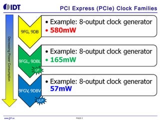
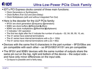
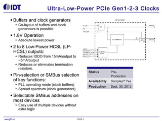
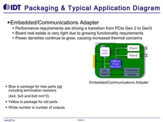
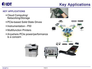
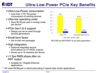
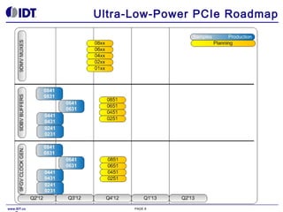
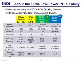
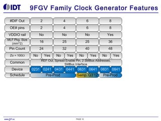
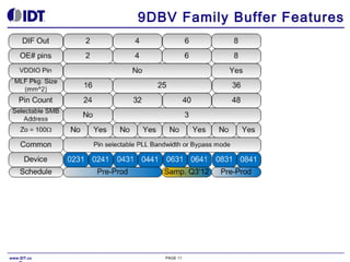
SlideShare a Scribd company logo
Ultra-Low-Power (ULP) Clocking Solutions
for PCI Express Gen 1-2-3
IDT 9DBVxxxx and 9FGVxxxx
August, 2012
Ron Wade
Technical Marketing Manger
Timing and Synchronization Division
Ron.Wade@idt.com

©2012 Integrated Device Technology, Inc.
PCI Express (PCIe) Clock Families

Decreasing Power Consumption

LP

ULP

www.IDT.co

PAGE 2
Ultra-Low-Power PCIe Clock Family
● IDT’s PCI Express clocks consist of three main functions:
● Clock Generators or Synthesizers
● Clock Buffers (Fan Out and Zero-Delay)
● Clock Multiplexers (with and without integrated Fan Out)
● Here is the decoder for the ULP PCIe family:
● 9FGV are clock generators (Frequency Generators)
● 9DBV are clock buffers (Differential Buffers)
● 9DMV are clock multiplexers (Differential Multiplexers)
● V indicates 1.8V operation
● The first two digits after the V indicate the number of outputs – 02, 04, 06, 09, 10, etc.
● The 31 series have external terminations
● The 41 series have internal terminations with a Zo = 100Ω
● The 51 series have internal terminations with a Zo = 85Ω
● Devices

with the same first 6 characters in the part number – 9FGV08xx are
pin compatible with each other – so 9FGV0831/41/51 are pin compatible

● The

9FGV and 9DBV devices with the same number of outputs share the
same pin out on the top, right and bottom of the device – the output side –
and have only minor differences on the input side.
●

Co-layout is possible and is fairly easy.

www.IDT.co

PAGE 3
Ultra-Low-Power PCIe Gen1-2-3 Clocks
● Buffers and clock generators
● Co-layout of buffers and clock
generators is possible
● 1.8V Operation
● Absolute lowest power
●2

to 8 Low-Power HCSL (LPHCSL) outputs:
●
●

Reduces IDDO from 15mA/output to
~5mA/output
Reduces or eliminates termination
resistors.

or SMBus selection
of key functions:
●
●

PLL operating mode (clock buffers)
Spread spectrum (clock generators)

● Selectable

SMBus addresses on
most devices
●

www.IDT.co

Easy use of multiple devices without
extra logic

PAGE 4

Status

PreProduction

Availability

Samples? Yes

Production

● Pin-selection

Sept. 30, 2012
Packaging & Typical Application Diagram
● Embedded/Communications
●
●
●

Adapter

Performance requirements are driving a transition from PCIe Gen 2 to Gen3
Board real estate is very tight due to growing functionality requirements
Power densities continue to grow, causing increased thermal concerns
PCIe IO

PCIe
PCIe
Switch
Switch

PCIe IO
Ultra Low
Ultra Low
Power
Power
PCIe Clock
PCIe Clock

CPU
Chipset

●

(4x4, 5x5 and 6x6 mm^2)
Yellow is package for old parts

●

White number is number of outputs

www.IDT.co

Memory

Embedded/Communications Adapter

Blue is package for new parts not
including termination resistors

●

Peripherals

PAGE 5
Key Applications
KEY APPLICATIONS
● Cloud

Computing/
Networking/Storage

● PCIe-based

Solid State Drives

● Instrumentation
● Multifunction

- PXI

Printers

● Anywhere

PCIe power/performance
is a concern

www.IDT.co

PAGE 6
Ultra-Low-Power PCIe Key Benefits
● Ultra-Low-Power consumption
● Less than 1/10th the power
consumption of existing devices
●

Ultra low operating costs
●

Save $0.45 per year in energy costs
per device*

● PCIe Gen1-2-3 support
● Design can be re-used through
several generations
● Small form factor
● 4x4 to 6x6 mm packages

9FG108 and 9FGV0831 8 o/p clock generators

● High integration
● Optional integrated source
terminations on LP-HCSL outputs
● Saves up to 16 resistors per device
● <1.5ps

RMS phase jitter on
REF output

Suitable for 1Gigabit Ethernet
applications
* 1W costs $0.86/year in electrical/cooling in typical data center applications
●

www.IDT.co

PAGE 7
Ultra-Low-Power PCIe Roadmap

www.IDT.co

PAGE 8
About the Ultra-Low-Power PCIe Family
● These
● All

devices are part of IDT’s PCIe Clocking Devices.

families offer PCIe Gen1-2-3 compliant devices.
9FGL LP
9DBL
9ZXL

ULP

557-xx
5V4106x
5V4123x

9FG
9DB
9ZX2

Power
Supply(ies)

3.3V

3.3V

3.3V Core
1.05V-3.3V O/P

1.8V Core
1.05V-1.8V O/P

Output Type

HCSL

HCSL

LP- HCSL

LP-HCSL

#Outputs

1-4

4-19

4-19

2-8 (initially)

REF output

No

Yes

No

Yes

Pin Counts
Packages

8-20
SOIC,
TSSOP,QF
N

28-72
TSSOP,
QFN

20-72
QFN

24-48
QFN

4 External

4 External

2 External or
0 External

2 External or
0 External

412mW
(4 O/P)

580mW

165mW

57mW

Term.
Resistors
(per Dif pair)
Power
(8 O/P Clock
Gen)
www.IDT.co

PAGE 9

9FGV
9DBV
9FGV Family Clock Generator Features

www.IDT.co

PAGE 10
9DBV Family Buffer Features

www.IDT.co

PAGE 11
Design Documentation
Visit www.idt.com for additional information

THANK YOU!

www.IDT.co

PAGE 12
Transcript
●

Hi, there. My name is Ron Wade, Technical Marketing Manager in the Timing and Synchronization Division of IDT. I'm going to give you a quick overview of our brand new ultra low power PCI
Express Timing Solutions family.

●

So, PCI Express can be thought of as having three generations of timing parts. The original technology was 3.3 volt HCSL output structure, which was developed in the early 2000's. For
comparison sake here I'm taking an eight output clock generator from each technology. You can see that in this case the 3.3 volt HCSL which is the yellow and black burns 580 milliwatts of
power to give you an eight output clock generator. In the mid 2000's, we developed a low-power HCSL output for use in notebook PC's, and normalizing to an eight output clock generator, that
technology was able to provide a reduced power consumption of 165 milliwatts. What we're introducing today is an ultra low power PCI Express family and again, an eight output clock
generator using the 9FGV or 9DBV devices which are the blue and white can give you that PCI Express Gen1, two, three clock generator for as little as 57 milliwatts. You can see that as we're
decreasing the power here significantly we're also still providing you with the PCI Express Gen1 to Gen2 to Gen3 capability.

●

So, the ultra low power PCI Express family consists of three main building blocks. There's the clock generators, there's the clock buffers, which are both fanout mode and zero delay, and the
clock multiplexers, which have a single output or they have integrated fanout. The ultra low power PCI Express family part numbers all kind of play together and hang together and once you
figure out the decoder ring, which is really simple here, you can kind of figure out what kind of part you need to plop into your design without any complicated selector guides. So, the FGV
parts for the clock generators, FG stands for frequency generator. The DBV parts are the clock buffers. DV stands for differential buffer. The DMV parts are the clock multiplexers, which
stands for differential multiplexers and the V indicates 1.8 volt operation. The first two digits are the V are the number of outputs, which currently range from two to eight, but will eventually
range from one to ten. The 31 series parts have external terminations. The 41 series parts have a 100 ohm differential output termination and the 51 series parts have an 85 ohm output
termination, to support the newer practices in PCI Express. So, devices with the first six characters in the part number say, 9FGV0831 or 41 or 51 are all compatible with each other except for
that difference in the output terminations. For parts that have the same number of outputs whether it's a buffer or a clock generator, the output side of the part is identical between them. So, an
831 clock generator and a 831 buffer, the top, the right side and the bottom of the parts are all the same pin out which makes it easy to switch from one to the other in co-layout.

●

So, the clocks as mentioned, the main functions are the buffers in the clock generators. These are 1.8 volt operation for the absolute lowest power consumption. We did do a lot of work to
actually reduce the current required and these devices do actually draw less current than the yellow and the green technology parts that I'd mentioned previously. So, again, the outputs are
two to eight today. They are low power HCSL which to the receiver looks exactly the same as the kind of legacy HCSL technology. The benefit here is that the current per output drops from 15
milliamps down to five and then we have the ability to integrate or have external the termination resistors. The other key thing we have is you may not have an SM bus handy and you don't
need an SM bus to control the basic functions of the parts. The clock generator, for instance, there's a spread enable pin that enables you to have not only spread off, but to have a quarter
percent down spread or half a percent down spread as a pin selection. Likewise, the buffers have a pin that allows you to select either high or low bandwidth or a bypass mode, which is a
fanout with the PLL, as the name implies, bypassed and turned off. Also, the device that synthesizers have, two selectable SM bus addresses so that you can use up to two of them on the
same segment. Most of the fanout buffers have three selectable SM bus addresses so that up to three of those devices can be used on the same SM bus segment and the buffers in the
synthesizer addresses do not overlap. It's very easy to have up to five of these devices on the same segment without any external logic. All the parts are pre-production right now, samples are
available now and will be in full production by the end of September.  

●

A typical application for these is an embedded communications adapter where you've got a PCI Express switch, PCI Express IO, a CPU chip set or an FPGA and various peripherals in
memory and performance requirements are from Gen1 to Gen2, going to Gen3. These parts cover the whole gambit of that performance envelope. The other thing in these types of
applications as you cram more and more functionality in the same space as board real estate becomes very tight. Also, power densities continue to grow and as the power density grows, then
thermal concerns tend to show up as well. So, these parts are available in commercial and industrial temperature ranges. They have a very low thermal profile and they are very small
package-wise. Package comparison, not including the external termination resistors and not including the leads of the packages is shown here, where the original yellow parts are the T-SOP
and SOIC-type packages. The blue boxes are the QFN's at the 9DBV and FGV parts come in. At the eight output level, a six by six millimeter QFN is significantly smaller than the original 48
pin T-SOP used by the eight output parts in the 3.3 volt HCSL range.

●

Key applications, again, these parts are very much at home in cloud computing and in networking and storage. They're finding a very nice reception in PCI Express-based solid state drives
due to their thermal characteristics, i.e. low power, pixie instrumentation, multi-function printers and basically anywhere where you need PC Express Gen1, 2, 3 with a very low power footprint.

●

The key benefits of the ultra low power PCI Express or certainly the power consumption, it's less than one-tenth of the comparable function in the original 3.3 volt HCSL technology. Lower
power consumption directly translates into lower operating cost. And using a benchmark of one watt cost 86 cents per year in a data center for not only the powering of the device, but the
cooling of the device. Saving one watt saves 86 cents a year. So, going from an eight output yellow synthesizer to an eight output blue synthesizer results in 45 cents a year in reduced energy
cost. These devices are PCI Express Gen1, 2, 3, which means that you can reuse the same device through multiple generations of your product. They're a small form factor. They're a four by
four to six by six millimeters QFN's today. We will have a three by three for some of the very small parts in the near future. They have high integration. We have integrated output terminations
for those environments where you're driving a homogeneous type of transmission line. In other words, all the transmissions lines are 100 ohm or 85 ohm. We also offer it without the internal
terminations for cases where you may need to terminate to different types of loads. The ref on the synthesizers or the clock generators is a copy of the crystal and it is less than 1.5
picoseconds RMS phase jitter which means that it is suitable for gigabit Ethernet, which adds more integration capability to this device for your design.

●

I'm not going to spend too much time on these slides. You can view these at your leisure. The clock generator family as it exists today, on August, 20, 2012 is shown here, where we segregate
the number of outputs and basically allow you to pick your device based on your particular application requirements. Then likewise, the differential buffer family features are shown here where
you've got the number of outputs, the number of OE pins, et cetera, end count, et cetera, et cetera, and schedule for the parts.

●

In closing, I'd like to mention you can go to www.IDT.com for additional information and I would like to extend a very warm thank you for taking time to learn about IDT's ultra low power PCI
Express Timing Solutions.

www.IDT.co

PAGE 13

More Related Content

What's hot

Energy Metering ICs with Active Real Power
Energy Metering ICs with Active Real PowerEnergy Metering ICs with Active Real Power
Energy Metering ICs with Active Real Power
Premier Farnell
 
Catálogo DDC con bus de datos y software para aeronáutica
Catálogo DDC con bus de datos y software para aeronáuticaCatálogo DDC con bus de datos y software para aeronáutica
Catálogo DDC con bus de datos y software para aeronáutica
Marketing Donalba
 
Bus de datos y Software de DDC
Bus de datos y Software de DDCBus de datos y Software de DDC
Bus de datos y Software de DDC
Marketing Donalba
 
The FlexTiles Development Platform offers Dual FPGA for 3D SoC Prototyping
The FlexTiles Development Platform offers Dual FPGA for 3D SoC PrototypingThe FlexTiles Development Platform offers Dual FPGA for 3D SoC Prototyping
The FlexTiles Development Platform offers Dual FPGA for 3D SoC Prototyping
FlexTiles Team
 
Shoftcore Processors
Shoftcore ProcessorsShoftcore Processors
Shoftcore Processors
Anish Goel
 
Atmel 2486-8-bit-avr-microcontroller-atmega8 l-datasheet
Atmel 2486-8-bit-avr-microcontroller-atmega8 l-datasheetAtmel 2486-8-bit-avr-microcontroller-atmega8 l-datasheet
Atmel 2486-8-bit-avr-microcontroller-atmega8 l-datasheet
sang2792
 
ARM COMPLETE DETAIL PART 4
ARM COMPLETE DETAIL PART 4ARM COMPLETE DETAIL PART 4
ARM COMPLETE DETAIL PART 4
NOWAY
 
I2C-Bus Design and Verification Specs
I2C-Bus Design and Verification SpecsI2C-Bus Design and Verification Specs
I2C-Bus Design and Verification Specs
Mostafa Khamis
 
Arm7 Interfacing examples
Arm7   Interfacing examples Arm7   Interfacing examples
Arm7 Interfacing examples
Dr.YNM
 
8051,chapter1,architecture and peripherals
8051,chapter1,architecture and peripherals8051,chapter1,architecture and peripherals
8051,chapter1,architecture and peripherals
amrutachintawar239
 
SoC FPGA Technology
SoC FPGA TechnologySoC FPGA Technology
SoC FPGA Technology
Siraj Muhammad
 
Profibus
ProfibusProfibus
Profibus
plc_course
 
LCD Interacing with 8051
LCD Interacing with 8051LCD Interacing with 8051
LCD Interacing with 8051
Sudhanshu Janwadkar
 
Microcontroller 8051 and its interfacing
Microcontroller 8051 and its interfacingMicrocontroller 8051 and its interfacing
Microcontroller 8051 and its interfacing
Ankur Mahajan
 
8051 archi
8051 archi8051 archi
8051 archi
VJ Aiswaryadevi
 
Microcontroller 8051
Microcontroller 8051Microcontroller 8051
Microcontroller 8051
guest70d48b1
 
AN INTEGRATED FOUR-PORT DC-DC CONVERTER-CEI0080
AN INTEGRATED FOUR-PORT DC-DC CONVERTER-CEI0080AN INTEGRATED FOUR-PORT DC-DC CONVERTER-CEI0080
AN INTEGRATED FOUR-PORT DC-DC CONVERTER-CEI0080
Vivek Venugopal
 
Introduction to Vortex86DX2 Motion-Control Evaluation Board
Introduction to Vortex86DX2 Motion-Control Evaluation BoardIntroduction to Vortex86DX2 Motion-Control Evaluation Board
Introduction to Vortex86DX2 Motion-Control Evaluation Board
roboard
 
Embedded &amp; pcb design
Embedded &amp; pcb designEmbedded &amp; pcb design
Embedded &amp; pcb design
Tanveer Behl
 
8096 microcontrollers notes
8096 microcontrollers notes8096 microcontrollers notes
8096 microcontrollers notes
Dr.YNM
 

What's hot (20)

Energy Metering ICs with Active Real Power
Energy Metering ICs with Active Real PowerEnergy Metering ICs with Active Real Power
Energy Metering ICs with Active Real Power
 
Catálogo DDC con bus de datos y software para aeronáutica
Catálogo DDC con bus de datos y software para aeronáuticaCatálogo DDC con bus de datos y software para aeronáutica
Catálogo DDC con bus de datos y software para aeronáutica
 
Bus de datos y Software de DDC
Bus de datos y Software de DDCBus de datos y Software de DDC
Bus de datos y Software de DDC
 
The FlexTiles Development Platform offers Dual FPGA for 3D SoC Prototyping
The FlexTiles Development Platform offers Dual FPGA for 3D SoC PrototypingThe FlexTiles Development Platform offers Dual FPGA for 3D SoC Prototyping
The FlexTiles Development Platform offers Dual FPGA for 3D SoC Prototyping
 
Shoftcore Processors
Shoftcore ProcessorsShoftcore Processors
Shoftcore Processors
 
Atmel 2486-8-bit-avr-microcontroller-atmega8 l-datasheet
Atmel 2486-8-bit-avr-microcontroller-atmega8 l-datasheetAtmel 2486-8-bit-avr-microcontroller-atmega8 l-datasheet
Atmel 2486-8-bit-avr-microcontroller-atmega8 l-datasheet
 
ARM COMPLETE DETAIL PART 4
ARM COMPLETE DETAIL PART 4ARM COMPLETE DETAIL PART 4
ARM COMPLETE DETAIL PART 4
 
I2C-Bus Design and Verification Specs
I2C-Bus Design and Verification SpecsI2C-Bus Design and Verification Specs
I2C-Bus Design and Verification Specs
 
Arm7 Interfacing examples
Arm7   Interfacing examples Arm7   Interfacing examples
Arm7 Interfacing examples
 
8051,chapter1,architecture and peripherals
8051,chapter1,architecture and peripherals8051,chapter1,architecture and peripherals
8051,chapter1,architecture and peripherals
 
SoC FPGA Technology
SoC FPGA TechnologySoC FPGA Technology
SoC FPGA Technology
 
Profibus
ProfibusProfibus
Profibus
 
LCD Interacing with 8051
LCD Interacing with 8051LCD Interacing with 8051
LCD Interacing with 8051
 
Microcontroller 8051 and its interfacing
Microcontroller 8051 and its interfacingMicrocontroller 8051 and its interfacing
Microcontroller 8051 and its interfacing
 
8051 archi
8051 archi8051 archi
8051 archi
 
Microcontroller 8051
Microcontroller 8051Microcontroller 8051
Microcontroller 8051
 
AN INTEGRATED FOUR-PORT DC-DC CONVERTER-CEI0080
AN INTEGRATED FOUR-PORT DC-DC CONVERTER-CEI0080AN INTEGRATED FOUR-PORT DC-DC CONVERTER-CEI0080
AN INTEGRATED FOUR-PORT DC-DC CONVERTER-CEI0080
 
Introduction to Vortex86DX2 Motion-Control Evaluation Board
Introduction to Vortex86DX2 Motion-Control Evaluation BoardIntroduction to Vortex86DX2 Motion-Control Evaluation Board
Introduction to Vortex86DX2 Motion-Control Evaluation Board
 
Embedded &amp; pcb design
Embedded &amp; pcb designEmbedded &amp; pcb design
Embedded &amp; pcb design
 
8096 microcontrollers notes
8096 microcontrollers notes8096 microcontrollers notes
8096 microcontrollers notes
 

Similar to PCI Express Clock Generators and Buffers by IDT: Ultra-low-power for PCIe Gen 1-2-3

Divya
DivyaDivya
Ppt embedded
Ppt embeddedPpt embedded
Ppt embedded
karan bansal
 
MPU and MCU IP Cores from CAST
MPU and MCU IP Cores from CASTMPU and MCU IP Cores from CAST
MPU and MCU IP Cores from CAST
CAST, Inc.
 
8051 microcontroller
8051 microcontroller8051 microcontroller
8051 microcontroller
Shubhrika Sehgal
 
Brochure (2016-01-30)
Brochure (2016-01-30)Brochure (2016-01-30)
Brochure (2016-01-30)
Jonah McLeod
 
Cisco router configuration
Cisco router configurationCisco router configuration
Cisco router configuration
vin424
 
Difference between i3 and i5 and i7 and core 2 duo
Difference between i3 and i5 and i7 and core 2 duoDifference between i3 and i5 and i7 and core 2 duo
Difference between i3 and i5 and i7 and core 2 duo
Shubham Singh
 
Difference between i3 and i5 and i7 and core 2 duo pdf
Difference between i3 and i5 and i7 and core 2 duo pdfDifference between i3 and i5 and i7 and core 2 duo pdf
Difference between i3 and i5 and i7 and core 2 duo pdf
navendu shekhar
 
Computer ogranization lecture (chapter 1 introduction)
Computer ogranization lecture (chapter 1   introduction)Computer ogranization lecture (chapter 1   introduction)
Computer ogranization lecture (chapter 1 introduction)
Nhelgane Hablo
 
Spartan-II FPGA (xc2s30)
Spartan-II FPGA (xc2s30)Spartan-II FPGA (xc2s30)
Spartan-II FPGA (xc2s30)
A B Shinde
 
INDUSTRIAL TRAINING REPORT EMBEDDED SYSTEM.pptx
INDUSTRIAL TRAINING REPORT EMBEDDED SYSTEM.pptxINDUSTRIAL TRAINING REPORT EMBEDDED SYSTEM.pptx
INDUSTRIAL TRAINING REPORT EMBEDDED SYSTEM.pptx
MeghdeepSingh
 
8051 Presentation
8051 Presentation8051 Presentation
8051 Presentation
Sayan Chakraborty
 
8 bit microcontroller
8 bit microcontroller8 bit microcontroller
8 bit microcontroller
محمدعبد الحى
 
Leakage power optimization for ripple carry adder
Leakage power optimization for ripple carry adder Leakage power optimization for ripple carry adder
Leakage power optimization for ripple carry adder
NAVEEN TOKAS
 
Hpe pro liant dl180 generation9 (gen9)
Hpe pro liant dl180 generation9 (gen9) Hpe pro liant dl180 generation9 (gen9)
Hpe pro liant dl180 generation9 (gen9)
Sourav Dash
 
MICROPROCESSOR_Notes.pptx
MICROPROCESSOR_Notes.pptxMICROPROCESSOR_Notes.pptx
MICROPROCESSOR_Notes.pptx
Workingad
 
Report on Embedded Based Home security system
Report on Embedded Based Home security systemReport on Embedded Based Home security system
Report on Embedded Based Home security system
NIT srinagar
 
IBM High IOPS MLC Adapters
IBM High IOPS MLC AdaptersIBM High IOPS MLC Adapters
IBM High IOPS MLC Adapters
IBM India Smarter Computing
 
embedded system introduction to microcontrollers
embedded system introduction to microcontrollersembedded system introduction to microcontrollers
embedded system introduction to microcontrollers
BarER4
 
AT89 S52
AT89 S52AT89 S52
AT89 S52
estherkakani
 

Similar to PCI Express Clock Generators and Buffers by IDT: Ultra-low-power for PCIe Gen 1-2-3 (20)

Divya
DivyaDivya
Divya
 
Ppt embedded
Ppt embeddedPpt embedded
Ppt embedded
 
MPU and MCU IP Cores from CAST
MPU and MCU IP Cores from CASTMPU and MCU IP Cores from CAST
MPU and MCU IP Cores from CAST
 
8051 microcontroller
8051 microcontroller8051 microcontroller
8051 microcontroller
 
Brochure (2016-01-30)
Brochure (2016-01-30)Brochure (2016-01-30)
Brochure (2016-01-30)
 
Cisco router configuration
Cisco router configurationCisco router configuration
Cisco router configuration
 
Difference between i3 and i5 and i7 and core 2 duo
Difference between i3 and i5 and i7 and core 2 duoDifference between i3 and i5 and i7 and core 2 duo
Difference between i3 and i5 and i7 and core 2 duo
 
Difference between i3 and i5 and i7 and core 2 duo pdf
Difference between i3 and i5 and i7 and core 2 duo pdfDifference between i3 and i5 and i7 and core 2 duo pdf
Difference between i3 and i5 and i7 and core 2 duo pdf
 
Computer ogranization lecture (chapter 1 introduction)
Computer ogranization lecture (chapter 1   introduction)Computer ogranization lecture (chapter 1   introduction)
Computer ogranization lecture (chapter 1 introduction)
 
Spartan-II FPGA (xc2s30)
Spartan-II FPGA (xc2s30)Spartan-II FPGA (xc2s30)
Spartan-II FPGA (xc2s30)
 
INDUSTRIAL TRAINING REPORT EMBEDDED SYSTEM.pptx
INDUSTRIAL TRAINING REPORT EMBEDDED SYSTEM.pptxINDUSTRIAL TRAINING REPORT EMBEDDED SYSTEM.pptx
INDUSTRIAL TRAINING REPORT EMBEDDED SYSTEM.pptx
 
8051 Presentation
8051 Presentation8051 Presentation
8051 Presentation
 
8 bit microcontroller
8 bit microcontroller8 bit microcontroller
8 bit microcontroller
 
Leakage power optimization for ripple carry adder
Leakage power optimization for ripple carry adder Leakage power optimization for ripple carry adder
Leakage power optimization for ripple carry adder
 
Hpe pro liant dl180 generation9 (gen9)
Hpe pro liant dl180 generation9 (gen9) Hpe pro liant dl180 generation9 (gen9)
Hpe pro liant dl180 generation9 (gen9)
 
MICROPROCESSOR_Notes.pptx
MICROPROCESSOR_Notes.pptxMICROPROCESSOR_Notes.pptx
MICROPROCESSOR_Notes.pptx
 
Report on Embedded Based Home security system
Report on Embedded Based Home security systemReport on Embedded Based Home security system
Report on Embedded Based Home security system
 
IBM High IOPS MLC Adapters
IBM High IOPS MLC AdaptersIBM High IOPS MLC Adapters
IBM High IOPS MLC Adapters
 
embedded system introduction to microcontrollers
embedded system introduction to microcontrollersembedded system introduction to microcontrollers
embedded system introduction to microcontrollers
 
AT89 S52
AT89 S52AT89 S52
AT89 S52
 

More from Integrated Device Technology

Single-Ended Fanout Buffers and Dividers by IDT
Single-Ended Fanout Buffers and Dividers by IDT Single-Ended Fanout Buffers and Dividers by IDT
Single-Ended Fanout Buffers and Dividers by IDT
Integrated Device Technology
 
Fanout Buffers by IDT - World Leader in Timing Solutions
Fanout Buffers by IDT - World Leader in Timing Solutions Fanout Buffers by IDT - World Leader in Timing Solutions
Fanout Buffers by IDT - World Leader in Timing Solutions
Integrated Device Technology
 
RF to IF Mixers by IDT: Low-power Downconversion Mixers with Zero-Distortion
RF to IF Mixers by IDT: Low-power Downconversion Mixers with Zero-DistortionRF to IF Mixers by IDT: Low-power Downconversion Mixers with Zero-Distortion
RF to IF Mixers by IDT: Low-power Downconversion Mixers with Zero-Distortion
Integrated Device Technology
 
IDT Wireless Power IDTP9020, IDTP9030 IC and Evaluation Kit Overview
IDT Wireless Power IDTP9020, IDTP9030 IC and Evaluation Kit OverviewIDT Wireless Power IDTP9020, IDTP9030 IC and Evaluation Kit Overview
IDT Wireless Power IDTP9020, IDTP9030 IC and Evaluation Kit Overview
Integrated Device Technology
 
Understanding and Testing DDR4 R-DIMM and LR-DIMM Technology
Understanding and Testing DDR4 R-DIMM and LR-DIMM TechnologyUnderstanding and Testing DDR4 R-DIMM and LR-DIMM Technology
Understanding and Testing DDR4 R-DIMM and LR-DIMM Technology
Integrated Device Technology
 
Introduction to IDT Wireless Power IC Solutions (Inductive Charging)
Introduction to IDT Wireless Power IC Solutions (Inductive Charging)Introduction to IDT Wireless Power IC Solutions (Inductive Charging)
Introduction to IDT Wireless Power IC Solutions (Inductive Charging)
Integrated Device Technology
 
89HT0832P 16-lane 8 Gbps PCIe 3.0 Retimer by IDT
89HT0832P 16-lane 8 Gbps PCIe 3.0 Retimer by IDT89HT0832P 16-lane 8 Gbps PCIe 3.0 Retimer by IDT
89HT0832P 16-lane 8 Gbps PCIe 3.0 Retimer by IDT
Integrated Device Technology
 
Introduction to Serial RapidIO® (SRIO) by IDT
Introduction to Serial RapidIO® (SRIO) by IDTIntroduction to Serial RapidIO® (SRIO) by IDT
Introduction to Serial RapidIO® (SRIO) by IDT
Integrated Device Technology
 

More from Integrated Device Technology (8)

Single-Ended Fanout Buffers and Dividers by IDT
Single-Ended Fanout Buffers and Dividers by IDT Single-Ended Fanout Buffers and Dividers by IDT
Single-Ended Fanout Buffers and Dividers by IDT
 
Fanout Buffers by IDT - World Leader in Timing Solutions
Fanout Buffers by IDT - World Leader in Timing Solutions Fanout Buffers by IDT - World Leader in Timing Solutions
Fanout Buffers by IDT - World Leader in Timing Solutions
 
RF to IF Mixers by IDT: Low-power Downconversion Mixers with Zero-Distortion
RF to IF Mixers by IDT: Low-power Downconversion Mixers with Zero-DistortionRF to IF Mixers by IDT: Low-power Downconversion Mixers with Zero-Distortion
RF to IF Mixers by IDT: Low-power Downconversion Mixers with Zero-Distortion
 
IDT Wireless Power IDTP9020, IDTP9030 IC and Evaluation Kit Overview
IDT Wireless Power IDTP9020, IDTP9030 IC and Evaluation Kit OverviewIDT Wireless Power IDTP9020, IDTP9030 IC and Evaluation Kit Overview
IDT Wireless Power IDTP9020, IDTP9030 IC and Evaluation Kit Overview
 
Understanding and Testing DDR4 R-DIMM and LR-DIMM Technology
Understanding and Testing DDR4 R-DIMM and LR-DIMM TechnologyUnderstanding and Testing DDR4 R-DIMM and LR-DIMM Technology
Understanding and Testing DDR4 R-DIMM and LR-DIMM Technology
 
Introduction to IDT Wireless Power IC Solutions (Inductive Charging)
Introduction to IDT Wireless Power IC Solutions (Inductive Charging)Introduction to IDT Wireless Power IC Solutions (Inductive Charging)
Introduction to IDT Wireless Power IC Solutions (Inductive Charging)
 
89HT0832P 16-lane 8 Gbps PCIe 3.0 Retimer by IDT
89HT0832P 16-lane 8 Gbps PCIe 3.0 Retimer by IDT89HT0832P 16-lane 8 Gbps PCIe 3.0 Retimer by IDT
89HT0832P 16-lane 8 Gbps PCIe 3.0 Retimer by IDT
 
Introduction to Serial RapidIO® (SRIO) by IDT
Introduction to Serial RapidIO® (SRIO) by IDTIntroduction to Serial RapidIO® (SRIO) by IDT
Introduction to Serial RapidIO® (SRIO) by IDT
 

Recently uploaded

GraphSummit Singapore | The Future of Agility: Supercharging Digital Transfor...
GraphSummit Singapore | The Future of Agility: Supercharging Digital Transfor...GraphSummit Singapore | The Future of Agility: Supercharging Digital Transfor...
GraphSummit Singapore | The Future of Agility: Supercharging Digital Transfor...
Neo4j
 
UiPath Test Automation using UiPath Test Suite series, part 6
UiPath Test Automation using UiPath Test Suite series, part 6UiPath Test Automation using UiPath Test Suite series, part 6
UiPath Test Automation using UiPath Test Suite series, part 6
DianaGray10
 
Why You Should Replace Windows 11 with Nitrux Linux 3.5.0 for enhanced perfor...
Why You Should Replace Windows 11 with Nitrux Linux 3.5.0 for enhanced perfor...Why You Should Replace Windows 11 with Nitrux Linux 3.5.0 for enhanced perfor...
Why You Should Replace Windows 11 with Nitrux Linux 3.5.0 for enhanced perfor...
SOFTTECHHUB
 
Best 20 SEO Techniques To Improve Website Visibility In SERP
Best 20 SEO Techniques To Improve Website Visibility In SERPBest 20 SEO Techniques To Improve Website Visibility In SERP
Best 20 SEO Techniques To Improve Website Visibility In SERP
Pixlogix Infotech
 
AI 101: An Introduction to the Basics and Impact of Artificial Intelligence
AI 101: An Introduction to the Basics and Impact of Artificial IntelligenceAI 101: An Introduction to the Basics and Impact of Artificial Intelligence
AI 101: An Introduction to the Basics and Impact of Artificial Intelligence
IndexBug
 
Cosa hanno in comune un mattoncino Lego e la backdoor XZ?
Cosa hanno in comune un mattoncino Lego e la backdoor XZ?Cosa hanno in comune un mattoncino Lego e la backdoor XZ?
Cosa hanno in comune un mattoncino Lego e la backdoor XZ?
Speck&Tech
 
How to use Firebase Data Connect For Flutter
How to use Firebase Data Connect For FlutterHow to use Firebase Data Connect For Flutter
How to use Firebase Data Connect For Flutter
Daiki Mogmet Ito
 
Unlock the Future of Search with MongoDB Atlas_ Vector Search Unleashed.pdf
Unlock the Future of Search with MongoDB Atlas_ Vector Search Unleashed.pdfUnlock the Future of Search with MongoDB Atlas_ Vector Search Unleashed.pdf
Unlock the Future of Search with MongoDB Atlas_ Vector Search Unleashed.pdf
Malak Abu Hammad
 
Removing Uninteresting Bytes in Software Fuzzing
Removing Uninteresting Bytes in Software FuzzingRemoving Uninteresting Bytes in Software Fuzzing
Removing Uninteresting Bytes in Software Fuzzing
Aftab Hussain
 
UiPath Test Automation using UiPath Test Suite series, part 5
UiPath Test Automation using UiPath Test Suite series, part 5UiPath Test Automation using UiPath Test Suite series, part 5
UiPath Test Automation using UiPath Test Suite series, part 5
DianaGray10
 
20240609 QFM020 Irresponsible AI Reading List May 2024
20240609 QFM020 Irresponsible AI Reading List May 202420240609 QFM020 Irresponsible AI Reading List May 2024
20240609 QFM020 Irresponsible AI Reading List May 2024
Matthew Sinclair
 
Artificial Intelligence for XMLDevelopment
Artificial Intelligence for XMLDevelopmentArtificial Intelligence for XMLDevelopment
Artificial Intelligence for XMLDevelopment
Octavian Nadolu
 
Building Production Ready Search Pipelines with Spark and Milvus
Building Production Ready Search Pipelines with Spark and MilvusBuilding Production Ready Search Pipelines with Spark and Milvus
Building Production Ready Search Pipelines with Spark and Milvus
Zilliz
 
20240607 QFM018 Elixir Reading List May 2024
20240607 QFM018 Elixir Reading List May 202420240607 QFM018 Elixir Reading List May 2024
20240607 QFM018 Elixir Reading List May 2024
Matthew Sinclair
 
National Security Agency - NSA mobile device best practices
National Security Agency - NSA mobile device best practicesNational Security Agency - NSA mobile device best practices
National Security Agency - NSA mobile device best practices
Quotidiano Piemontese
 
Uni Systems Copilot event_05062024_C.Vlachos.pdf
Uni Systems Copilot event_05062024_C.Vlachos.pdfUni Systems Copilot event_05062024_C.Vlachos.pdf
Uni Systems Copilot event_05062024_C.Vlachos.pdf
Uni Systems S.M.S.A.
 
Observability Concepts EVERY Developer Should Know -- DeveloperWeek Europe.pdf
Observability Concepts EVERY Developer Should Know -- DeveloperWeek Europe.pdfObservability Concepts EVERY Developer Should Know -- DeveloperWeek Europe.pdf
Observability Concepts EVERY Developer Should Know -- DeveloperWeek Europe.pdf
Paige Cruz
 
Mind map of terminologies used in context of Generative AI
Mind map of terminologies used in context of Generative AIMind map of terminologies used in context of Generative AI
Mind map of terminologies used in context of Generative AI
Kumud Singh
 
TrustArc Webinar - 2024 Global Privacy Survey
TrustArc Webinar - 2024 Global Privacy SurveyTrustArc Webinar - 2024 Global Privacy Survey
TrustArc Webinar - 2024 Global Privacy Survey
TrustArc
 
Introduction to CHERI technology - Cybersecurity
Introduction to CHERI technology - CybersecurityIntroduction to CHERI technology - Cybersecurity
Introduction to CHERI technology - Cybersecurity
mikeeftimakis1
 

Recently uploaded (20)

GraphSummit Singapore | The Future of Agility: Supercharging Digital Transfor...
GraphSummit Singapore | The Future of Agility: Supercharging Digital Transfor...GraphSummit Singapore | The Future of Agility: Supercharging Digital Transfor...
GraphSummit Singapore | The Future of Agility: Supercharging Digital Transfor...
 
UiPath Test Automation using UiPath Test Suite series, part 6
UiPath Test Automation using UiPath Test Suite series, part 6UiPath Test Automation using UiPath Test Suite series, part 6
UiPath Test Automation using UiPath Test Suite series, part 6
 
Why You Should Replace Windows 11 with Nitrux Linux 3.5.0 for enhanced perfor...
Why You Should Replace Windows 11 with Nitrux Linux 3.5.0 for enhanced perfor...Why You Should Replace Windows 11 with Nitrux Linux 3.5.0 for enhanced perfor...
Why You Should Replace Windows 11 with Nitrux Linux 3.5.0 for enhanced perfor...
 
Best 20 SEO Techniques To Improve Website Visibility In SERP
Best 20 SEO Techniques To Improve Website Visibility In SERPBest 20 SEO Techniques To Improve Website Visibility In SERP
Best 20 SEO Techniques To Improve Website Visibility In SERP
 
AI 101: An Introduction to the Basics and Impact of Artificial Intelligence
AI 101: An Introduction to the Basics and Impact of Artificial IntelligenceAI 101: An Introduction to the Basics and Impact of Artificial Intelligence
AI 101: An Introduction to the Basics and Impact of Artificial Intelligence
 
Cosa hanno in comune un mattoncino Lego e la backdoor XZ?
Cosa hanno in comune un mattoncino Lego e la backdoor XZ?Cosa hanno in comune un mattoncino Lego e la backdoor XZ?
Cosa hanno in comune un mattoncino Lego e la backdoor XZ?
 
How to use Firebase Data Connect For Flutter
How to use Firebase Data Connect For FlutterHow to use Firebase Data Connect For Flutter
How to use Firebase Data Connect For Flutter
 
Unlock the Future of Search with MongoDB Atlas_ Vector Search Unleashed.pdf
Unlock the Future of Search with MongoDB Atlas_ Vector Search Unleashed.pdfUnlock the Future of Search with MongoDB Atlas_ Vector Search Unleashed.pdf
Unlock the Future of Search with MongoDB Atlas_ Vector Search Unleashed.pdf
 
Removing Uninteresting Bytes in Software Fuzzing
Removing Uninteresting Bytes in Software FuzzingRemoving Uninteresting Bytes in Software Fuzzing
Removing Uninteresting Bytes in Software Fuzzing
 
UiPath Test Automation using UiPath Test Suite series, part 5
UiPath Test Automation using UiPath Test Suite series, part 5UiPath Test Automation using UiPath Test Suite series, part 5
UiPath Test Automation using UiPath Test Suite series, part 5
 
20240609 QFM020 Irresponsible AI Reading List May 2024
20240609 QFM020 Irresponsible AI Reading List May 202420240609 QFM020 Irresponsible AI Reading List May 2024
20240609 QFM020 Irresponsible AI Reading List May 2024
 
Artificial Intelligence for XMLDevelopment
Artificial Intelligence for XMLDevelopmentArtificial Intelligence for XMLDevelopment
Artificial Intelligence for XMLDevelopment
 
Building Production Ready Search Pipelines with Spark and Milvus
Building Production Ready Search Pipelines with Spark and MilvusBuilding Production Ready Search Pipelines with Spark and Milvus
Building Production Ready Search Pipelines with Spark and Milvus
 
20240607 QFM018 Elixir Reading List May 2024
20240607 QFM018 Elixir Reading List May 202420240607 QFM018 Elixir Reading List May 2024
20240607 QFM018 Elixir Reading List May 2024
 
National Security Agency - NSA mobile device best practices
National Security Agency - NSA mobile device best practicesNational Security Agency - NSA mobile device best practices
National Security Agency - NSA mobile device best practices
 
Uni Systems Copilot event_05062024_C.Vlachos.pdf
Uni Systems Copilot event_05062024_C.Vlachos.pdfUni Systems Copilot event_05062024_C.Vlachos.pdf
Uni Systems Copilot event_05062024_C.Vlachos.pdf
 
Observability Concepts EVERY Developer Should Know -- DeveloperWeek Europe.pdf
Observability Concepts EVERY Developer Should Know -- DeveloperWeek Europe.pdfObservability Concepts EVERY Developer Should Know -- DeveloperWeek Europe.pdf
Observability Concepts EVERY Developer Should Know -- DeveloperWeek Europe.pdf
 
Mind map of terminologies used in context of Generative AI
Mind map of terminologies used in context of Generative AIMind map of terminologies used in context of Generative AI
Mind map of terminologies used in context of Generative AI
 
TrustArc Webinar - 2024 Global Privacy Survey
TrustArc Webinar - 2024 Global Privacy SurveyTrustArc Webinar - 2024 Global Privacy Survey
TrustArc Webinar - 2024 Global Privacy Survey
 
Introduction to CHERI technology - Cybersecurity
Introduction to CHERI technology - CybersecurityIntroduction to CHERI technology - Cybersecurity
Introduction to CHERI technology - Cybersecurity
 

PCI Express Clock Generators and Buffers by IDT: Ultra-low-power for PCIe Gen 1-2-3

  • 1. Ultra-Low-Power (ULP) Clocking Solutions for PCI Express Gen 1-2-3 IDT 9DBVxxxx and 9FGVxxxx August, 2012 Ron Wade Technical Marketing Manger Timing and Synchronization Division Ron.Wade@idt.com ©2012 Integrated Device Technology, Inc.
  • 2. PCI Express (PCIe) Clock Families Decreasing Power Consumption LP ULP www.IDT.co PAGE 2
  • 3. Ultra-Low-Power PCIe Clock Family ● IDT’s PCI Express clocks consist of three main functions: ● Clock Generators or Synthesizers ● Clock Buffers (Fan Out and Zero-Delay) ● Clock Multiplexers (with and without integrated Fan Out) ● Here is the decoder for the ULP PCIe family: ● 9FGV are clock generators (Frequency Generators) ● 9DBV are clock buffers (Differential Buffers) ● 9DMV are clock multiplexers (Differential Multiplexers) ● V indicates 1.8V operation ● The first two digits after the V indicate the number of outputs – 02, 04, 06, 09, 10, etc. ● The 31 series have external terminations ● The 41 series have internal terminations with a Zo = 100Ω ● The 51 series have internal terminations with a Zo = 85Ω ● Devices with the same first 6 characters in the part number – 9FGV08xx are pin compatible with each other – so 9FGV0831/41/51 are pin compatible ● The 9FGV and 9DBV devices with the same number of outputs share the same pin out on the top, right and bottom of the device – the output side – and have only minor differences on the input side. ● Co-layout is possible and is fairly easy. www.IDT.co PAGE 3
  • 4. Ultra-Low-Power PCIe Gen1-2-3 Clocks ● Buffers and clock generators ● Co-layout of buffers and clock generators is possible ● 1.8V Operation ● Absolute lowest power ●2 to 8 Low-Power HCSL (LPHCSL) outputs: ● ● Reduces IDDO from 15mA/output to ~5mA/output Reduces or eliminates termination resistors. or SMBus selection of key functions: ● ● PLL operating mode (clock buffers) Spread spectrum (clock generators) ● Selectable SMBus addresses on most devices ● www.IDT.co Easy use of multiple devices without extra logic PAGE 4 Status PreProduction Availability Samples? Yes Production ● Pin-selection Sept. 30, 2012
  • 5. Packaging & Typical Application Diagram ● Embedded/Communications ● ● ● Adapter Performance requirements are driving a transition from PCIe Gen 2 to Gen3 Board real estate is very tight due to growing functionality requirements Power densities continue to grow, causing increased thermal concerns PCIe IO PCIe PCIe Switch Switch PCIe IO Ultra Low Ultra Low Power Power PCIe Clock PCIe Clock CPU Chipset ● (4x4, 5x5 and 6x6 mm^2) Yellow is package for old parts ● White number is number of outputs www.IDT.co Memory Embedded/Communications Adapter Blue is package for new parts not including termination resistors ● Peripherals PAGE 5
  • 6. Key Applications KEY APPLICATIONS ● Cloud Computing/ Networking/Storage ● PCIe-based Solid State Drives ● Instrumentation ● Multifunction - PXI Printers ● Anywhere PCIe power/performance is a concern www.IDT.co PAGE 6
  • 7. Ultra-Low-Power PCIe Key Benefits ● Ultra-Low-Power consumption ● Less than 1/10th the power consumption of existing devices ● Ultra low operating costs ● Save $0.45 per year in energy costs per device* ● PCIe Gen1-2-3 support ● Design can be re-used through several generations ● Small form factor ● 4x4 to 6x6 mm packages 9FG108 and 9FGV0831 8 o/p clock generators ● High integration ● Optional integrated source terminations on LP-HCSL outputs ● Saves up to 16 resistors per device ● <1.5ps RMS phase jitter on REF output Suitable for 1Gigabit Ethernet applications * 1W costs $0.86/year in electrical/cooling in typical data center applications ● www.IDT.co PAGE 7
  • 9. About the Ultra-Low-Power PCIe Family ● These ● All devices are part of IDT’s PCIe Clocking Devices. families offer PCIe Gen1-2-3 compliant devices. 9FGL LP 9DBL 9ZXL ULP 557-xx 5V4106x 5V4123x 9FG 9DB 9ZX2 Power Supply(ies) 3.3V 3.3V 3.3V Core 1.05V-3.3V O/P 1.8V Core 1.05V-1.8V O/P Output Type HCSL HCSL LP- HCSL LP-HCSL #Outputs 1-4 4-19 4-19 2-8 (initially) REF output No Yes No Yes Pin Counts Packages 8-20 SOIC, TSSOP,QF N 28-72 TSSOP, QFN 20-72 QFN 24-48 QFN 4 External 4 External 2 External or 0 External 2 External or 0 External 412mW (4 O/P) 580mW 165mW 57mW Term. Resistors (per Dif pair) Power (8 O/P Clock Gen) www.IDT.co PAGE 9 9FGV 9DBV
  • 10. 9FGV Family Clock Generator Features www.IDT.co PAGE 10
  • 11. 9DBV Family Buffer Features www.IDT.co PAGE 11
  • 12. Design Documentation Visit www.idt.com for additional information THANK YOU! www.IDT.co PAGE 12
  • 13. Transcript ● Hi, there. My name is Ron Wade, Technical Marketing Manager in the Timing and Synchronization Division of IDT. I'm going to give you a quick overview of our brand new ultra low power PCI Express Timing Solutions family. ● So, PCI Express can be thought of as having three generations of timing parts. The original technology was 3.3 volt HCSL output structure, which was developed in the early 2000's. For comparison sake here I'm taking an eight output clock generator from each technology. You can see that in this case the 3.3 volt HCSL which is the yellow and black burns 580 milliwatts of power to give you an eight output clock generator. In the mid 2000's, we developed a low-power HCSL output for use in notebook PC's, and normalizing to an eight output clock generator, that technology was able to provide a reduced power consumption of 165 milliwatts. What we're introducing today is an ultra low power PCI Express family and again, an eight output clock generator using the 9FGV or 9DBV devices which are the blue and white can give you that PCI Express Gen1, two, three clock generator for as little as 57 milliwatts. You can see that as we're decreasing the power here significantly we're also still providing you with the PCI Express Gen1 to Gen2 to Gen3 capability. ● So, the ultra low power PCI Express family consists of three main building blocks. There's the clock generators, there's the clock buffers, which are both fanout mode and zero delay, and the clock multiplexers, which have a single output or they have integrated fanout. The ultra low power PCI Express family part numbers all kind of play together and hang together and once you figure out the decoder ring, which is really simple here, you can kind of figure out what kind of part you need to plop into your design without any complicated selector guides. So, the FGV parts for the clock generators, FG stands for frequency generator. The DBV parts are the clock buffers. DV stands for differential buffer. The DMV parts are the clock multiplexers, which stands for differential multiplexers and the V indicates 1.8 volt operation. The first two digits are the V are the number of outputs, which currently range from two to eight, but will eventually range from one to ten. The 31 series parts have external terminations. The 41 series parts have a 100 ohm differential output termination and the 51 series parts have an 85 ohm output termination, to support the newer practices in PCI Express. So, devices with the first six characters in the part number say, 9FGV0831 or 41 or 51 are all compatible with each other except for that difference in the output terminations. For parts that have the same number of outputs whether it's a buffer or a clock generator, the output side of the part is identical between them. So, an 831 clock generator and a 831 buffer, the top, the right side and the bottom of the parts are all the same pin out which makes it easy to switch from one to the other in co-layout. ● So, the clocks as mentioned, the main functions are the buffers in the clock generators. These are 1.8 volt operation for the absolute lowest power consumption. We did do a lot of work to actually reduce the current required and these devices do actually draw less current than the yellow and the green technology parts that I'd mentioned previously. So, again, the outputs are two to eight today. They are low power HCSL which to the receiver looks exactly the same as the kind of legacy HCSL technology. The benefit here is that the current per output drops from 15 milliamps down to five and then we have the ability to integrate or have external the termination resistors. The other key thing we have is you may not have an SM bus handy and you don't need an SM bus to control the basic functions of the parts. The clock generator, for instance, there's a spread enable pin that enables you to have not only spread off, but to have a quarter percent down spread or half a percent down spread as a pin selection. Likewise, the buffers have a pin that allows you to select either high or low bandwidth or a bypass mode, which is a fanout with the PLL, as the name implies, bypassed and turned off. Also, the device that synthesizers have, two selectable SM bus addresses so that you can use up to two of them on the same segment. Most of the fanout buffers have three selectable SM bus addresses so that up to three of those devices can be used on the same SM bus segment and the buffers in the synthesizer addresses do not overlap. It's very easy to have up to five of these devices on the same segment without any external logic. All the parts are pre-production right now, samples are available now and will be in full production by the end of September.   ● A typical application for these is an embedded communications adapter where you've got a PCI Express switch, PCI Express IO, a CPU chip set or an FPGA and various peripherals in memory and performance requirements are from Gen1 to Gen2, going to Gen3. These parts cover the whole gambit of that performance envelope. The other thing in these types of applications as you cram more and more functionality in the same space as board real estate becomes very tight. Also, power densities continue to grow and as the power density grows, then thermal concerns tend to show up as well. So, these parts are available in commercial and industrial temperature ranges. They have a very low thermal profile and they are very small package-wise. Package comparison, not including the external termination resistors and not including the leads of the packages is shown here, where the original yellow parts are the T-SOP and SOIC-type packages. The blue boxes are the QFN's at the 9DBV and FGV parts come in. At the eight output level, a six by six millimeter QFN is significantly smaller than the original 48 pin T-SOP used by the eight output parts in the 3.3 volt HCSL range. ● Key applications, again, these parts are very much at home in cloud computing and in networking and storage. They're finding a very nice reception in PCI Express-based solid state drives due to their thermal characteristics, i.e. low power, pixie instrumentation, multi-function printers and basically anywhere where you need PC Express Gen1, 2, 3 with a very low power footprint. ● The key benefits of the ultra low power PCI Express or certainly the power consumption, it's less than one-tenth of the comparable function in the original 3.3 volt HCSL technology. Lower power consumption directly translates into lower operating cost. And using a benchmark of one watt cost 86 cents per year in a data center for not only the powering of the device, but the cooling of the device. Saving one watt saves 86 cents a year. So, going from an eight output yellow synthesizer to an eight output blue synthesizer results in 45 cents a year in reduced energy cost. These devices are PCI Express Gen1, 2, 3, which means that you can reuse the same device through multiple generations of your product. They're a small form factor. They're a four by four to six by six millimeters QFN's today. We will have a three by three for some of the very small parts in the near future. They have high integration. We have integrated output terminations for those environments where you're driving a homogeneous type of transmission line. In other words, all the transmissions lines are 100 ohm or 85 ohm. We also offer it without the internal terminations for cases where you may need to terminate to different types of loads. The ref on the synthesizers or the clock generators is a copy of the crystal and it is less than 1.5 picoseconds RMS phase jitter which means that it is suitable for gigabit Ethernet, which adds more integration capability to this device for your design. ● I'm not going to spend too much time on these slides. You can view these at your leisure. The clock generator family as it exists today, on August, 20, 2012 is shown here, where we segregate the number of outputs and basically allow you to pick your device based on your particular application requirements. Then likewise, the differential buffer family features are shown here where you've got the number of outputs, the number of OE pins, et cetera, end count, et cetera, et cetera, and schedule for the parts. ● In closing, I'd like to mention you can go to www.IDT.com for additional information and I would like to extend a very warm thank you for taking time to learn about IDT's ultra low power PCI Express Timing Solutions. www.IDT.co PAGE 13

Editor's Notes

  1. 8 output devices are used for sake of comparison. All device are running from either 3.3V or 1.8V. Additional power savings are available on the L and V series devices if the differential outputs are powered from 1.05V instead of the core VDD voltage of 1.8V or 3.3V. We have achieved as low as 43 mW in the V series for customer specific applications. Beyond Green to Blue!
  2. Package out lines are for the packages only and do not include the termination resistors. When this factored in, even more board space is saved.
  3. 1W costs $0.86/year in electrical/cooling in typical data center applications Power consumption is directly proportional to operating costs.
  4. 9FGV are synthesizers 9DBV are buffers 9DMV are muxes 31 series has external terminations 41 series has differential Zo = 100 ohms 51 series has differential Zo = 85 ohms