Downloaded 312 times

![TWO-PHASE NON OVERLAPPING CLOCK GENERATOR WITH BUFFERED OUTPUT
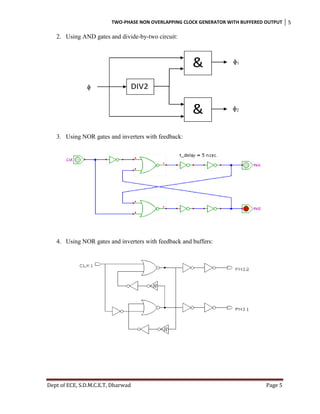
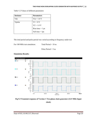
5. Using NAND gates and inverters with feedback:
All the above mentioned above circuit designs (except (1) and (2)) share similarity with
Kevin Karplus’s circuit designs [1]. Several researchers have even proposed robust design
which incorporates adjustable duty cycle [2] and programmable two phase non overlapping
clock generators [3]. The amount of research work done on this particular topic clearly shows
the importance of two-phase clocking circuits. In this mini project the focus is laid on
designing a simple two-phase non overlapping circuit generating clock signals, which
performs reasonably well with relatively large capacitive load at frequencies up to 100MHz.
Dept of ECE, S.D.M.C.E.T, Dharwad
Page 6
6](https://image.slidesharecdn.com/project-20report-2-131226062049-phpapp01/85/Design-of-Two-phase-non-overlapping-low-frequency-clock-generator-using-Cadence-Virtuoso-EDA-tools-6-320.jpg)
![TWO-PHASE NON OVERLAPPING CLOCK GENERATOR WITH BUFFERED OUTPUT
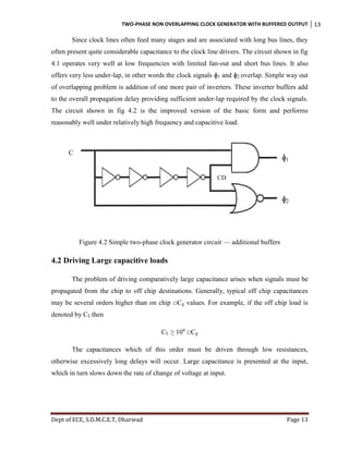
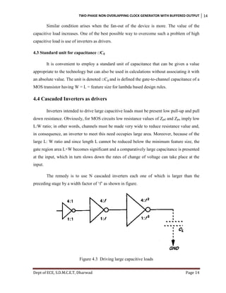
Clearly as the width factor increases, so the capacitive load presented at the inverter
input increases and the area occupied increases also. Equally clearly, the rate at which width
increases will influence the number N of stages which must be cascaded to drive a particular
value of CL. Thus with large f, N decreases but delay per stage increases.
Delay per CMOS pair = 7fτ.
y = CL/□Cg = fN
Therefore the choice of f and N are interdependent.
Determine the value of f which will minimize the overall delay for a given value of y.
Apply logarithms on both side of the equation
ln(y) = N ln(f)
i.e.
N = ln(y)/ln(f)
For N even (CMOS)
Total delay = N/2 (7fτ)
= 3.5Nfτ
From above relations, we can write
Delay α Nfτ = [ln(y)/ln(f)] fτ
It can be shown that total delay is minimized if f assumes the value of e for CMOS inverters.
Assume f = e, we have
N = ln(y)/ln(e)
i.e. N = ln(y)
Overall delay td
td = 3.5 eNτ (CMOS)
N even:
N odd:
( for logical transition 0 to 1)
Dept of ECE, S.D.M.C.E.T, Dharwad
td = [3.5(N-1)+2] eτ (CMOS)
Page 15
15](https://image.slidesharecdn.com/project-20report-2-131226062049-phpapp01/85/Design-of-Two-phase-non-overlapping-low-frequency-clock-generator-using-Cadence-Virtuoso-EDA-tools-15-320.jpg)
![TWO-PHASE NON OVERLAPPING CLOCK GENERATOR WITH BUFFERED OUTPUT
(for logical transition 1 to 0)
td = [3.5(N-1) +5] eτ (CMOS)
4.5 Race conditions
In general, race condition refers to a situation in which the result depends upon the sequence
in which events happen. In particular, a race condition occurs when a system/device is
designed assuming a particular sequence of events without taking steps to ensure it. In logic
gates, it happens when the inputs arrive at the gate in a sequence not assumed while deriving
the function. This results, sometimes, in the anomalous behavior of the logic gate because of
the unexpected dependence on the sequence of arrival of inputs. Since, the function of the
logic gate is calculated assuming static inputs; the order of arrival may have impact on the
output. We can consider race condition as a situation in which two or more signals are racing
to have their effect on the output. This is how; race condition derives its name.
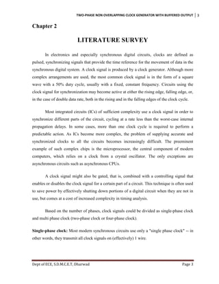
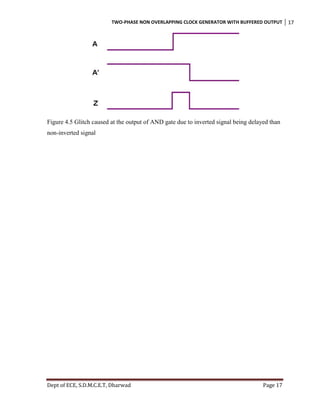
For a very simple example, consider the following logic function: Z = A˖A’
Figure 4.4 Circuit having race condition
Theoretically, the output will always be ‘0’. However, this is true only if the noninverted portion of the signal has greater delay in reaching the AND gate (we have
considered ‘0’ -> ‘1’ transition of the input signal ‘A’). As shown in the figure above, the
signal passing through inverter will have some delay of its own. If the signal through inverter
reaches the AND gate later than the one without inverter, there will be a glitch as shown in
the figure 2. For ‘1’ -> ‘0’ transition, the opposite will happen.
If the condition for race is violated, as shown in fig 4.5, the design may enter an
undefined state, the one which might not have been considered while designing. Hence, the
whole system will malfunction in such a scenario leading to failure. It might be the case that
some elements in the design enter metastable state, which can further cause problems. Hence,
it is very important to give proper consideration to race conditions.
Dept of ECE, S.D.M.C.E.T, Dharwad
Page 16
16](https://image.slidesharecdn.com/project-20report-2-131226062049-phpapp01/85/Design-of-Two-phase-non-overlapping-low-frequency-clock-generator-using-Cadence-Virtuoso-EDA-tools-16-320.jpg)
![TWO-PHASE NON OVERLAPPING CLOCK GENERATOR WITH BUFFERED OUTPUT
REFERENCES
[1] “A programmable clock oscillator for integrated sensor applications”, Electron Devices
Meeting, 1998. Proceedings. 1998 IEEE Hong Kong.
[2] Magnus Karlsso, Mark Vesterbacka and Wlodek Kulesza, “A non-overlapping two-phase
clock generator With adjustable duty cycle”
[3] R. Długosz, K. Iniewski, T. Talaśka3, “0.35 μm 22μW Multiphase Programmable Clock
Generator for Circular Memory SC FIR Filter For Wireless Sensor Applications”,
Published in IEEE Workshop on Signal Processing Systems (SIPS) IM3, M3-5, 157-160,
2006.
[4] Douglas A. Pucknell and Kamran Eshraghian , “Basic Vlsi Design”, Third edition, PHI
Private Limited, 1994.
[5] Rajalaxmi Das, Ghanshyam Kumar Singh & Ram Mohan Mehra, “Two-Phase Clocking
Scheme for Low-Power and High-Speed VLSI”, International Journal of Advances in
Engineering & Technology, Volume 2, issue 1, 2011
Dept of ECE, S.D.M.C.E.T, Dharwad
Page 29
29](https://image.slidesharecdn.com/project-20report-2-131226062049-phpapp01/85/Design-of-Two-phase-non-overlapping-low-frequency-clock-generator-using-Cadence-Virtuoso-EDA-tools-29-320.jpg)

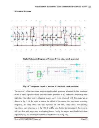
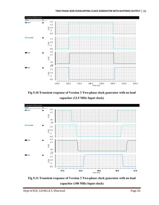
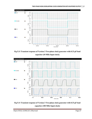
This document describes designing a two-phase non-overlapping clock generator circuit with buffered outputs. The circuit is required to generate clean square wave clock signals from a single-phase input clock between 10-100MHz. The output signals must drive a 0.33pF capacitive load without distortion. The design will be implemented using Cadence tools and modified through simulation to meet the objectives of generating true non-overlapping signals with at least 1ns of underlap that can operate over the specified frequency range and drive the required load.


![[IJET-V1I3P5] Authors :Dushyant Kumar Soni, Ashish Hiradhar](https://cdn.slidesharecdn.com/ss_thumbnails/ijet-v1i3p5-150519153226-lva1-app6891-thumbnail.jpg?width=640&height=640&fit=bounds)