1. Static timing analysis is a methodology for verifying timing characteristics of a design without test vectors, which is faster than simulation and guarantees 100% coverage of timing paths.
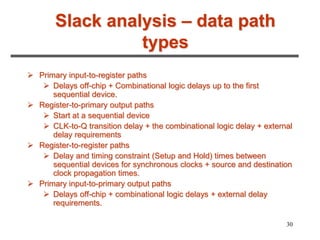
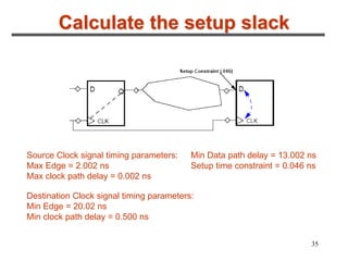
2. It involves breaking a circuit into timing paths, calculating the delay of each path, and checking if delays meet constraints. Timing paths are grouped by controlling clocks.
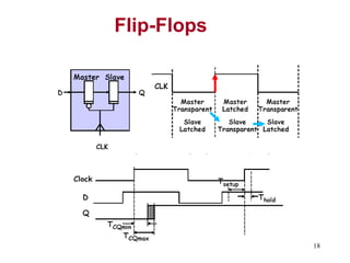
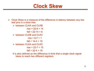
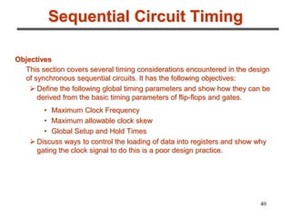
3. The maximum clock frequency is limited by flip-flop and gate delays. Clock skew between flip-flops must be less than the minimum setup/hold times to meet timing.
ROLE OF DIGITAL SIMULATION IN CONFIGURING NETWORK PARAMETERSDeepak Shankar
Selecting the right Ethernet standard and configuring all the network devices in the embedded systems accurately is an extremely hard and rigorous job. The configuration depends on the topology, workloads of the connected devices, processing overhead at the switches, and the external interfaces. Network calculus, mathematical models and analytical techniques provide worst case execution time (WCET), but their probability of activity is extremely wide. This leads to overdesign which leads to higher costs, power consumption, weight, and size. Simulating the network is the best way to measure the throughput of the entire system. Digital system simulation provides better latency and throughput accuracy, but the accuracy is still limited because it does not consider the latency associated with the network OS, cybersecurity processing and scheduling. In many cases, these factors can reduce the throughput by 20-40%.
In this paper, we will present our research on modeling the entire Ethernet network, including the workloads, network flow control, scheduling, switch hardware, and software. To substantially increase the coverage and compare topologies, we have developed a set of benchmarks that provides coverage for different combination of deterministic, rate-constrained, and best effort traffic. During the presentation, we will cover the benchmarks, the list of attributes required to accurately model the traffic, nodes, switches, and the scheduler settings. We will also look at the statistics and reports required to make the configuration decision. In addition, we will discuss how the model must be constructed to study the impact of future requirements, failures, network intrusions, and security detection schemes.
Key Takeaways:
1. Learn how to efficiently use network simulation to design Ethernet systems
2. Develop a reusable benchmark and associated statistics to test different configurations
3. The role and impact of the CDT slots, guard band, send slope, idle slope, shuffle scheduling, flow control and virtual channels
Clock tree synthesis (CTS) plays an important role in building well-balanced clock tree, fixing timing violations and reducing the extra unnecessary pessimism in the design. The goal during building a clock tree is to reduce the skew, maintain symmetrical clock tree structure and to cover all the registers in the design. We have captured some problematic scenarios and the problem solving approaches in this article.
Clock tree network enables in making design clean from a timing perspective. However, it is responsible for more than one third of the total power consumption of the chip. The impact of variations in the clock path is more than 2 times the other paths in the design. These variations in-turn affects the timing paths. Let us take an example; Due to the variation, if the clock path to the launching register is slowed down by 100ps and the clock path to the capturing register is fastened by 100ps then it impacts the setup constraint by adding 200ps more to it, this in-turn affects the timing path by making it more critical. Here we can see the importance of building a balanced clock tree. We will discuss on the timing improvements and methods to reduce the variations in the clock tree. The steps followed in building a customized clock tree and the steps followed to bring down the variations in the clock tree has been depicted in the following sections.
Accurate Synchronization of EtherCAT Systems Using Distributed ClocksDesign World
Synchronization and determinism are important considerations when selecting an industrial control system and the associated fieldbus. Additionally, it’s important for field devices to have network-wide interrupts for activating outputs, capturing input data, oversampling or latching events. These are all significant facets in the overall network synchronization scheme.
This webinar on Tuesday, Oct. 23 at 2 PM EST will explain how the Distributed Clock mechanism in EtherCAT works to meet all of these functions using properties inherent to the protocol. This can be done using a standard Ethernet network adaptor, all without the overhead of IEEE 1588.
Attend this webinar to learn:
How Distributed Clocks (DCs) in EtherCAT facilitate measurement of propagation delay throughout the system and synchronize network devices to a single time value
What EtherCAT slave devices can do to facilitate temporal behavior for outputs and inputs as well as implementing data oversampling
More about some of the concepts that enable EtherCAT to have a high scan rate as well as high levels of synchronization
Scan design is currently the most popular structured DFT approach. It is implemented by Connecting selected storage elements present in the design into multiple shift registers, called Scan chains.
Scannability Rules -->
The tool perform basic two check
1) It ensures all the defined clocks including set/Reset are at their off-states, the sequential element remain stable and inactive. (S1)
2) It ensures for each defined clocks can capture data when all other defined clocks are off. (S2)
Level sensitive scan design(LSSD) and Boundry scan(BS)Praveen Kumar
This presentation contains,
Introduction,design for testability, scan chain, operation, scan structure, test vectors, Boundry scan, test logic, operation, BS cell, states of TAP controller, Boundry scan instructions.
Introduction to Data Acquisition System
Introduction to Plant Information system
System Analysis
System Design and Implementation
System Integration and Testing
Results
Conclusion
Further Enhancement
Tutorial: The Role of Event-Time Analysis Order in Data StreamingVincenzo Gulisano
Slides for our tutorial, titled “The Role of Event-Time Analysis Order in Data Streaming”, presented at the 14th ACM International Conference on Distributed and Event-Based Systems (DEBS) conference. We have recorded the tutorial, and you can find the videos at the following links:
Part 1: https://youtu.be/SW_WS6ULsdY
Part 2: https://youtu.be/bq3ECNvPwOU
You can find this slides, as well as the code examples, at https://github.com/vincenzo-gulisano/debs2020_tutorial_event_time and at SlideS
Read| The latest issue of The Challenger is here! We are thrilled to announce that our school paper has qualified for the NATIONAL SCHOOLS PRESS CONFERENCE (NSPC) 2024. Thank you for your unwavering support and trust. Dive into the stories that made us stand out!
Acetabularia Information For Class 9 .docxvaibhavrinwa19
Acetabularia acetabulum is a single-celled green alga that in its vegetative state is morphologically differentiated into a basal rhizoid and an axially elongated stalk, which bears whorls of branching hairs. The single diploid nucleus resides in the rhizoid.
Macroeconomics- Movie Location
This will be used as part of your Personal Professional Portfolio once graded.
Objective:
Prepare a presentation or a paper using research, basic comparative analysis, data organization and application of economic information. You will make an informed assessment of an economic climate outside of the United States to accomplish an entertainment industry objective.
How to Make a Field invisible in Odoo 17Celine George
It is possible to hide or invisible some fields in odoo. Commonly using “invisible” attribute in the field definition to invisible the fields. This slide will show how to make a field invisible in odoo 17.
The Roman Empire A Historical Colossus.pdfkaushalkr1407
The Roman Empire, a vast and enduring power, stands as one of history's most remarkable civilizations, leaving an indelible imprint on the world. It emerged from the Roman Republic, transitioning into an imperial powerhouse under the leadership of Augustus Caesar in 27 BCE. This transformation marked the beginning of an era defined by unprecedented territorial expansion, architectural marvels, and profound cultural influence.
The empire's roots lie in the city of Rome, founded, according to legend, by Romulus in 753 BCE. Over centuries, Rome evolved from a small settlement to a formidable republic, characterized by a complex political system with elected officials and checks on power. However, internal strife, class conflicts, and military ambitions paved the way for the end of the Republic. Julius Caesar’s dictatorship and subsequent assassination in 44 BCE created a power vacuum, leading to a civil war. Octavian, later Augustus, emerged victorious, heralding the Roman Empire’s birth.
Under Augustus, the empire experienced the Pax Romana, a 200-year period of relative peace and stability. Augustus reformed the military, established efficient administrative systems, and initiated grand construction projects. The empire's borders expanded, encompassing territories from Britain to Egypt and from Spain to the Euphrates. Roman legions, renowned for their discipline and engineering prowess, secured and maintained these vast territories, building roads, fortifications, and cities that facilitated control and integration.
The Roman Empire’s society was hierarchical, with a rigid class system. At the top were the patricians, wealthy elites who held significant political power. Below them were the plebeians, free citizens with limited political influence, and the vast numbers of slaves who formed the backbone of the economy. The family unit was central, governed by the paterfamilias, the male head who held absolute authority.
Culturally, the Romans were eclectic, absorbing and adapting elements from the civilizations they encountered, particularly the Greeks. Roman art, literature, and philosophy reflected this synthesis, creating a rich cultural tapestry. Latin, the Roman language, became the lingua franca of the Western world, influencing numerous modern languages.
Roman architecture and engineering achievements were monumental. They perfected the arch, vault, and dome, constructing enduring structures like the Colosseum, Pantheon, and aqueducts. These engineering marvels not only showcased Roman ingenuity but also served practical purposes, from public entertainment to water supply.
Unit 8 - Information and Communication Technology (Paper I).pdfThiyagu K
This slides describes the basic concepts of ICT, basics of Email, Emerging Technology and Digital Initiatives in Education. This presentations aligns with the UGC Paper I syllabus.
The French Revolution, which began in 1789, was a period of radical social and political upheaval in France. It marked the decline of absolute monarchies, the rise of secular and democratic republics, and the eventual rise of Napoleon Bonaparte. This revolutionary period is crucial in understanding the transition from feudalism to modernity in Europe.
For more information, visit-www.vavaclasses.com
Palestine last event orientationfvgnh .pptxRaedMohamed3
An EFL lesson about the current events in Palestine. It is intended to be for intermediate students who wish to increase their listening skills through a short lesson in power point.
2. 2
Introduction
Effective methodology for verifying the timing characteristics of a
design without the use of test vectors
Conventional verification techniques are inadequate for complex
designs
Simulation time using conventional simulators
Thousands of test vectors are required to test all timing paths
using logic simulation
Increasing design complexity & smaller process technologies
Increases the number of iterations for STA
3. 3
Simulation vs. Static timing
0% 100%
Timing Simulation
(adding vectors)
Static timing analysis
(eliminating false paths)
True timing paths False timing paths
STA approach typically takes a fraction of the time it takes to run
logic simulation on a large design and guarantees 100% coverage
of all true timing paths in the design without having to generate test
vectors
5. 5
• Requires extensive vector creation
• Valid for FPGAs and smaller ASICs
• Falls apart on multi-million gate ASICs
OVERVIEW
6. 6
What is Static Timing Analysis?
Static Timing Analysis is a method for determining if a
circuit meets timing constraints without having to
simulate
Much faster than timing-driven, gate-level simulation
Proper circuit functionality is not checked
Vector generation NOT required
7. 7
STA in ASIC Design Flow – Pre
layout
Logic Synthesis
Design For test
Floor planning
Constraints
(clocks, input drive,
output load)
Static Timing Analysis
(estimated parasitics)
8. 8
STA in ASIC Design Flow –
Post Layout
Floor planning
Clock Tree Synthesis
Place and Route
Parasitic Extraction
SDF
(extracted parasitics)
Constraints
(clocks, input drive,
output load)
Static Timing Analysis
(estimated parasitics)
Static Timing Analysis
(extracted parasitics)
9. 9
2 Types of Timing Verification
Dynamic Timing Simulation
Advantages
Can be very accurate (spice-level)
Disadvantages
Analysis quality depends on stimulus vectors
Non-exhaustive, slow
Examples:
VCS,Spice,ACE
11. 11
Three Steps in Static Timing Analysis
Circuit is broken down into sets of timing paths
Delay of each path is calculated
Path delays are checked to see if timing constraints
have been met
12. 12
What is a Timing Path?
A Timing Path is a point-to-point path in a design which
can propagate data from one flip-flop to another
Each path has a start point and an endpoint
Start point:
Input ports Clock pins of flip-flops
Endpoints:
Output ports Data input pins of flip-flops
13. 13
Organizing Timing Paths Into Groups
Timing paths are grouped into path groups by the
clocks controlling their endpoints
Synthesis tools like PrimeTime and Design
Compiler organize timing reports by path groups
14. 14
Net and Cell Timing Arcs
The actual path delay is the sum of net and cell
delays along the timing path
15. 15
Net and Cell Delay
“Net Delay” refers to the total time needed to charge or
discharge all of the parasitics of a given net
Total net parasitics are affected by
net length
net fanout
Net delay and parasitics are typically
Back-Annotated (Post-Layout) from data obtained from
an extraction tool
Estimated (Pre-Layout)
16. 16
Cell Delay
In ASICs, the delay of a cell is affected by:
The input transition time (or slew rate)
The total load “seen” by the output transistors
Net capacitance and “downstream” pin capacitances
These will affect how quickly the input and output transistors
can “switch”
Inherent transistor delays and “internal” net delays
17. 17
Transparent Latch, Level Sensitive
– data passes through when clock high, latched when clock low
Clocked Storage Elements
D-Type Register or Flip-Flop, Edge-Triggered
– data captured on rising edge of clock, held for rest of cycle
19. 19
Basic terminologies
Pulse Width
Setup & Hold times
Signal slew
Clock latency
Clock Skew
Input arrival time
Output required time
Slack and Critical path
Recovery & Removal
times
False paths
Multi-cycle paths
20. 20
Pulse Width
Pulse width
It is the time between the active and inactive states of the same
signal
21. 21
Setup and Hold time
Setup time
For an edge triggered sequential element, the setup time is the time
interval before the active clock edge during which the data should
remain unchanged
Hold time
Time interval after the active clock edge during which the data
should remain unchanged
Both the above 2 timing violations can occur in a design when
clock path delay > data path delay
22. 22
Signal Slew
Signal (Clock/Data) slew
Amount of time it takes for a signal transition to occur
Accounts for uncertainty in Rise and fall times of the signal
Slew rate is measured in volts/sec
23. 23
Clock Latency
Clock Latency
Difference between the reference (source) clock slew to the clock
tree endpoint signal slew values
Rise latency and fall latency are specified
INV
Rise=7
Fall=4
Rise=7
Fall=4
Rise=7
Fall=4
Rise=7
Fall=4
Rise=7
Fall=4
Rise=7
Fall=4
Rise=7
Fall=4
CLK
CLKA
CLKB
CLKC
INV
INV
INV
INV
INV
BUF
BUF
25. 25
Clock Skew
Clock Skew is a measure of the difference in latency between any two
leaf pins in a clock tree.
between CLKA and CLKB
rise = 22-8 = 14
fall = 22-14 = 8
between CLKB and CLKC
rise = 8-7 = 1
fall = 14-4 = 10
between CLKA and CLKC
rise = 22-7 = 15
fall = 22-4 = 18
It is also defined as the difference in time that a single clock signal
takes to reach two different registers
26. 26
Input Arrival time
Input Arrival time
An arrival time defines the time interval during which a data signal
can arrive at an input pin in relation to the nearest edge of the clock
signal that triggers the data transition
28. 28
Slack and Critical path
Slack
It is the difference between the required (constraint) time and the
arrival time (inputs and delays).
Negative slack indicates that constraints have not been met, while
positive slack indicates that constraints have been met.
Slack analysis is used to identify timing critical paths in a design by
the static timing analysis tool
Critical path
Any logical path in the design that violates the timing constraints
Path with a negative slack
30. 30
Slack analysis – data path
types
Primary input-to-register paths
Delays off-chip + Combinational logic delays up to the first
sequential device.
Register-to-primary output paths
Start at a sequential device
CLK-to-Q transition delay + the combinational logic delay + external
delay requirements
Register-to-register paths
Delay and timing constraint (Setup and Hold) times between
sequential devices for synchronous clocks + source and destination
clock propagation times.
Primary input-to-primary output paths
Delays off-chip + combinational logic delays + external delay
requirements.
31. 31
Hold Slack calculation
Actual data arrival time definition
Data Input Arrival Timemin + Data path delaymin
If the data path starts in a primary input,
Data Input arrivalmin = Input arrival timemin
If the data path starts at a register,
(Source Clock Edgemin + Source Clock Path Delaymin) =
Data Input Arrivalmin
Required Stability time definition
(Destination Clock Edgemax + Destination Clock Path Delaymax) +
Hold = Required Stability Timemax
Hold Slack definition
Actual Data Arrivalmin - Required Stability Timemax
32. 32
Calculate the hold slack
Source Clock signal timing parameters:
Min Edge = 8.002 ns
Min clock path delay = 0.002 ns
Destination Clock signal timing parameters:
Max Edge = 2.020 ns
Max clock path delay = 0.500 ns
Min Data path delay = 0.802 ns
Hold time constraint = 1.046 ns
34. 34
Setup Slack calculation
Actual data arrival time definition
Data Input Arrival Timemax + Data path delaymax
If the data path starts in a primary input,
Data Input arrivalmax = Input arrival timemax
If the data path starts at a register,
(Source Clock Edgemax + Source Clock Path Delaymax) =
Data Input Arrivalmax
Required Stability time definition
(Destination Clock Edgemin + Destination Clock Path Delaymin) -
Setup = Required Stability Timemin
Setup slack definition
Required Stability Timemin - Actual Data Arrivalmax
35. 35
Calculate the setup slack
Source Clock signal timing parameters:
Max Edge = 2.002 ns
Max clock path delay = 0.002 ns
Destination Clock signal timing parameters:
Min Edge = 20.02 ns
Min clock path delay = 0.500 ns
Min Data path delay = 13.002 ns
Setup time constraint = 0.046 ns
37. 37
Recovery and Removal time
Recovery time
Like setup time for asynchronous port (set, reset)
Removal time
Like hold time for asynchronous port (set, reset)
Recovery time
It is the time available between the asynchronous signal going inactive
to the active clock edge
Removal time
It is the time between active clock edge and asynchronous signal
going inactive
38. 38
False Paths
False paths
Paths that physically exist in a design but are not logic/functional
paths
These paths never get sensitized under any input conditions
Mux 1
C C1 C2
A
B
Mux 2
S
B1 B2
OUT
40. 40
Sequential Circuit Timing
Objectives
This section covers several timing considerations encountered in the design
of synchronous sequential circuits. It has the following objectives:
Define the following global timing parameters and show how they can be
derived from the basic timing parameters of flip-flops and gates.
• Maximum Clock Frequency
• Maximum allowable clock skew
• Global Setup and Hold Times
Discuss ways to control the loading of data into registers and show why
gating the clock signal to do this is a poor design practice.
41. 41
Maximum Clock Frequency
The clock frequency for a synchronous sequential circuit is limited by
the timing parameters of its flip-flops and gates. This limit is called the
maximum clock frequency for the circuit. The minimum clock period is
the reciprocal of this frequency.
Relevant timing parameters
Gates:
• Propagation delays: min tPLH, min tPHL, max tPLH, max tPHL
Flip-Flops:
• Propagation delays: min tPLH, min tPHL, max tPLH, max tPHL
• Setup time: tsu
• Hold time: th
42. 42
Example
TW ≥ max tPFF + tsu
For the 7474, max tPLH = 25ns, max tPHL = 40ns, tsu = 20ns
TW ≥ max (max tPLH + tsu, max tPHL + tsu)
TW ≥ max (25+20, 40+20) = 60
D Q
Q
CK
Q
45. 45
Example
Paths from Q1 to Q1:
Paths from Q1 to Q2:
Paths from Q2 to Q1:
Paths from Q2 to Q2:
None
TW ≥ max tPDFF +tJKsu = 20 +10 = 30 ns
TW ≥ max tPDFF + max tAND + tJKsu = 20 + 12 + 10 = 42 ns
TW ≥ max tPJKFF + tOR + TDsu = 25 + 10 + 5 = 40 ns
TW ≥ max tPJKFF + max tAND + tJKsu = 25 + 12 + 10 = 47 ns
TW ≥ 47 ns
46. 46
If a clock edge does not arrive at different flip-flops at exactly the same
time, then the clock is said to be skewed between these flip-flops. The
difference between the times of arrival at the flip-flops is said to be the
amount of clock skew.
Clock skew is due to different delays on different paths from the clock
generator to the various flip-flops.
• Different length wires (wires have delay)
• Gates (buffers) on the paths
• Flip-Flops that clock on different edges (need to invert clock for
some flip-flops)
• Gating the clock to control loading of registers (a very bad idea)
Clock Skew
47. 47
• Example (Effect of clock skew on clock rate)
Clock C2 skewed after C1
Q1
Q2
D Q
Q
D Q
Q
CK
C1
C2
D2
TW ≥ max TPFF + max tOR + tsu
(if clock not skewed, i.e., tINV = 0)
TW ≥ max TPFF + max tOR + tsu - min tINV
(if clock skewed, i.e., tINV > 0)
48. 48
Clock C1 skewed after C2
Q1
Q2
D Q
Q
D Q
Q
CK
C1
C2
D2
TW ≥ max TPFF + max tOR + tsu
(if clock not skewed, i.e., tINV = 0)
TW ≥ max TPFF + max tOR + tsu + max tINV
(if clock skewed, i.e., tINV > 0)
49. 49
Summary of maximum clock frequency calculations
D Q
Logic
Network
D Q
C1 C2
Q1 D2
C1
Q1
D2
C2
TW
tPFF tOR tsu
tSK = tINV
C1
Q1
D2
C2
TW
tPFF tOR
tsu
tSK = tINV
C2 skewed after C1: TW ≥ max TPFF + max tNET + tsu - min tINV
C2 skewed before C1: TW ≥ max TPFF + max tNET + tsu + max tINV
50. 50
Maximum Allowable Clock Skew
How much skew between C1 and C2 can be tolerated in the following
circuit?
– Case 1: C2 delayed after C1
D Q
Q
D Q
Q
C2
Q1 D2
C1
tPFF > th + tSK
tSK < min tPFF - th
51. 51
Case 2: C1 delayed from C2
D Q
Q
D Q
Q
C2
Q1 D2
C1
52. 52
How does additional delay between the flip-flops affect the skew
calculations?
tSK ≤ min tPFF - th
tsk ≤ min tPFF + min tMUX - th
53. 53
Summary of allowable clock skew calculations
tSK + th ≤ tPFF + tNET
tSK ≤ min tPFF + min tNET - th
54. 54
Example: What is the minimum clock period for the following circuit under
the assumption that the clock C2 is skewed after C1 (i.e., C2 is delayed
from C1)?
N1
N2
C1 C2
Q1 D2 Q2
D1
D Q
Q
D Q
Q
55. 55
First calculate the maximum allowable clock skew.
Next calculate the minimum clock period due to the path from Q1 to D2.
Finally calculate the minimum clock period due to the path from Q2 to
D1
N1
N2
C1 C2
Q1 D2 Q2
D1
D Q
Q
D Q
Q
tSK < min tPFF + min tN1 - th
TW > max tPFF + max tN1 + tsu - min tSK
TW > max tPFF + max tN1 + tsu + max tSK
TW > max tPFF + max tN2 + tsu + (min tPFF + min tN1 - th)
TW > max tPFF + min tPFF + max tN2 + min tN1 + tsu - th
56. 56
Global Setup Time, Hold Time
and Propagation Delay
Global setup and hold times (data delayed)
TSU = tsu + max tNET
TH = th - min tNET
D Q
Q
X
CK
NET D
CLK
57. 57
Global setup & hold time (clock delayed)
D Q
Q
CK
D
CLK
TSU = tsu - min tC TH = th + max tC
58. 58
Global setup & hold time (data & clock delayed)
D Q
Q
X
CK
NET D
CLK
TSU = + max =-0987654321 - min . TH = th - min tNET + max tC
60. 60
Summary of global timing parameters
TSU = tsu + max tPN - min tPC ≤ tsu + max tPN
TH = th + max tPC - min tPN ≤ th + max tPC
TP = tPFF + tPN + tPC
61. 61
Example
Find TSU and TH for input signal LD relative to CLK.
LD
D
CLK
CK
Q
D Q
Q
TSU = tsu +max tNET - min tC
TH = th - min tNET + max tC
= tsu + max tINV + max tNAND + max tNAND - min tINV
= th - min tNAND - min tNAND + max TINV
62. 62
Register load control (gating the clock
• A very bad way to add a load control signal LD to a register that does not
have one is shown below
• The reason this is such a bad idea is illustrated by the following timing
diagram.
• The flip-flop sees two rising edges and will trigger twice. The only one we
want is the second one.
D
LD
CLK
CK
D Q
Q
63. 63
If LD was constrained to only change when the clock was low, then the only
problem would be the clock skew.
64. 64
If gating the clock is the only way to control the loading of registers, then
use the following approach:
There is still clock skew, but at least we only have one triggering edge.
D
LD
CLK
D Q
Q
65. 65
The best way to add a LD control signal is as follows:
LD
D
CLK
D Q
Q
66. 66
Tips & Tricks
Use timing diagrams to determine the timing properties of sequential circuits
Using typical timing values from the data sheet (use only max and/or min
values)
Gating the clock
67. 67
Detecting timing violations –
CASE 1
clk10Mhtz
clk20Mhtzref
Delay (min) = 5 ns
DFF 2
DFF 1
Data
(a) Hold time for clocks is 1.5 ns
Determine if there are any timing violations in this design
68. 68
Detecting timing violations –
CASE 2
Delay (min) = 5 ns
clk10Mhtz
clk20Mhtzref
DFF 2
DFF 1
Data
(a) Hold time for clocks is 1.5 ns
(b) Clock skew of 3.72 ns between clk20mref and clk10mz
Determine if there are any timing violations in this design
69. 69
Detecting timing violations –
CASE 3
(a) Hold time for clocks is 1.5 ns
(b) Clock skew of 3.72 ns between clk20mref and clk10mz
clk10Mhtz
clk20Mhtzref
DFF 2
DFF 1
Data
Delay (min) = 5 ns
70. 70
Detecting timing violations –
CASE 4
Consider
(a) Clock skew of 3.72 ns between clk20mref and clk10mz
(b) Clock network delays
clk10Mhtz
clk20Mhtzref
DFF 2
DFF 1
Data
Delay (min) = 5 ns
Propagation delay = 2 ns
(thru clock tree buffers)
Propagation delay = 4 ns
(thru clock tree buffers)