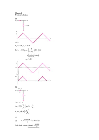
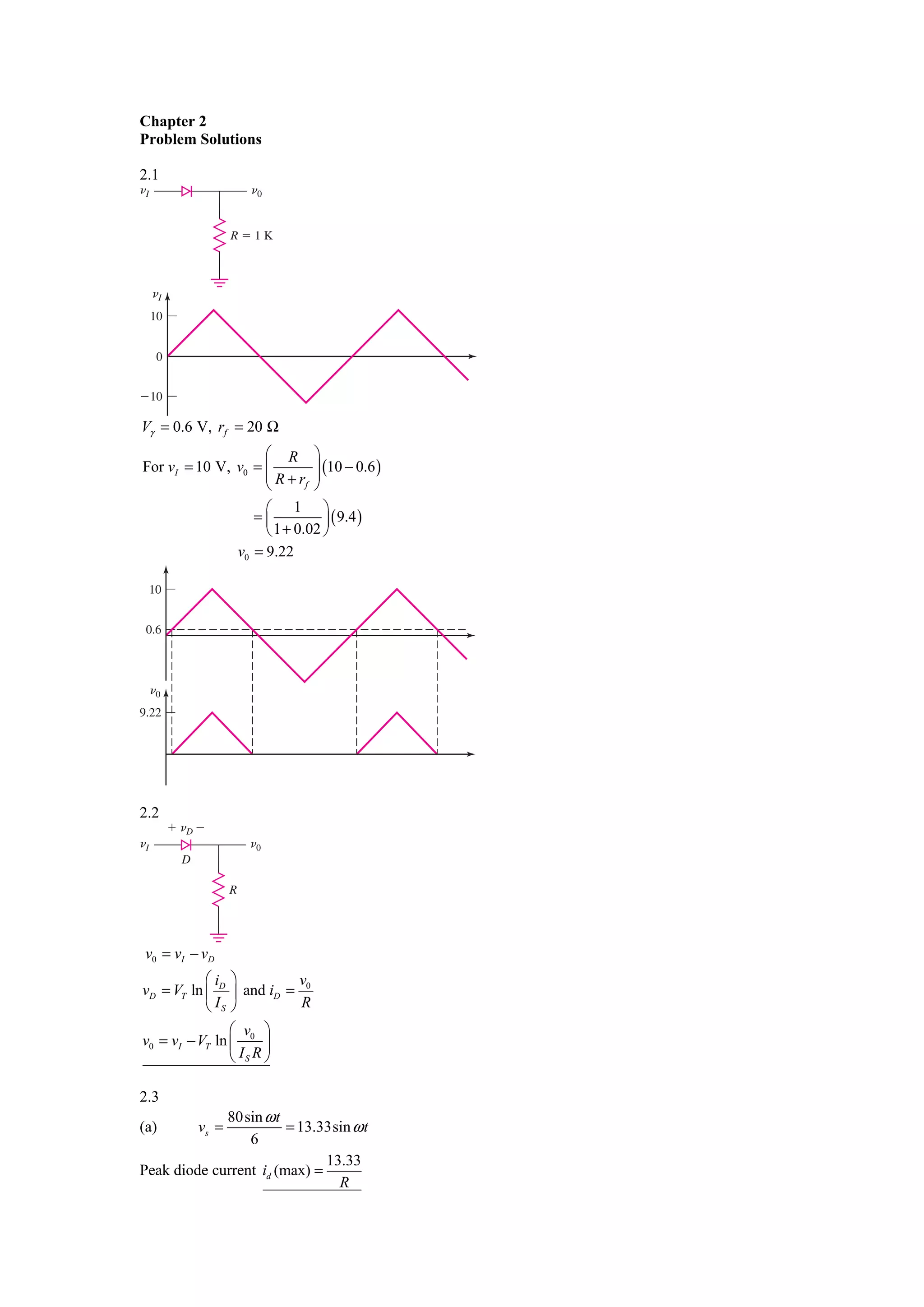
This document contains solutions to various circuit analysis problems. Problem 2.1 solves for the output voltage of a voltage divider circuit given input and resistor values. Problem 2.2 analyzes a circuit with a diode and calculates the output voltage as a function of the input voltage and diode characteristics. The remaining problems continue analyzing circuits involving resistors, diodes, capacitors and calculating values such as output voltage, current, power dissipation and more. Equations are provided and used to solve for unknown variables in each circuit.
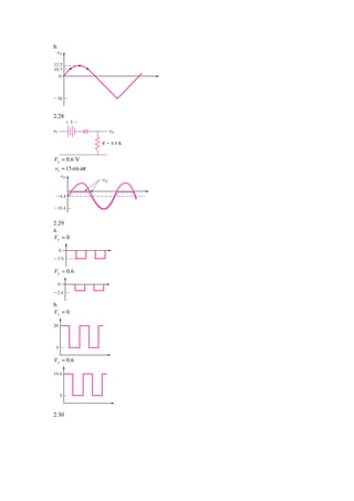
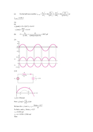
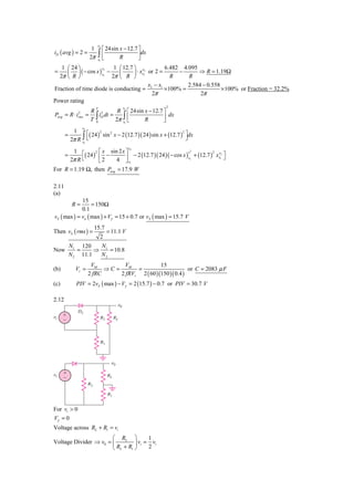
![(b) PIV = vs (max) = 13.3 V
(c)
To π
1 1
vo ( avg ) = ∫ v (t )dt = 2π ∫ 13.33sin × dt
o
To o o
13.33 13.33 13.33
[ − cos x ]o =
π
= ⎡ − ( −1 − 1) ⎤ =
⎣ ⎦
2π 2π π
vo ( avg ) = 4.24 V
(d) 50%
2.4
v0 = vS − 2Vγ ⇒ vS ( max ) = v0 ( max ) + 2Vγ
a. For v0 ( max ) = 25 V ⇒ vS ( max ) = 25 + 2 ( 0.7 ) = 26.4 V
N1 160 N
= ⇒ 1 = 6.06
N 2 26.4 N2
b. For v0 ( max ) = 100 V ⇒ vS ( max ) = 101.4 V
N1 160 N
= ⇒ 1 = 1.58
N 2 101.4 N2
From part (a) PIV = 2vS ( max ) − Vγ = 2 ( 26.4 ) − 0.7
or PIV = 52.1 V or, from part (b) PIV = 2 (101.4 ) − 0.7 or PIV = 202.1 V
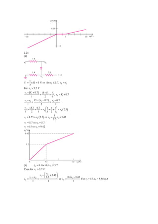
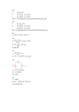
2.5
(a)
vs (max) = 12 + 2(0.7) = 13.4 V
13.4
vs ( rms ) = ⇒ vs (rms) = 9.48 V
2
(b)
VM VM
Vr = ⇒C =
2 f RC 2 f Vr R
12
C= ⇒ C = 2222 μ F
2 ( 60 )( 0.3)(150 )
(c)
VM ⎡ 2VM ⎤
id , peak = ⎢1 + π ⎥
R ⎢⎣ Vr ⎥⎦
12 ⎡ 2 (12 ) ⎤
= ⎢1 + π ⎥
150 ⎢ 0.3 ⎥
⎣ ⎦
id , peak = 2.33 A
2.6
(a)
vS ( max ) = 12 + 0.7 = 12.7 V
vS ( max )
vS ( rms ) = ⇒ vS ( rms ) = 8.98 V
2
VM V 12
(b) Vr = ⇒C = M = or C = 4444 μ F
fRC fRVr ( 60 )(150 )( 0.3)](https://image.slidesharecdn.com/ch02s-120608121817-phpapp02/85/Ch02s-2-320.jpg)
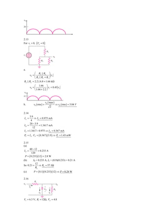
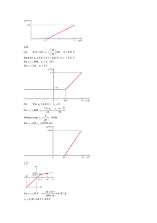
![a.
6.3 − 4.8
II = ⇒ 125 mA
12
I L = I I − I Z = 125 − I Z
25 ≤ I L ≤ 120 mA ⇒ 40 ≤ RL ≤ 192Ω
b.
PZ = I Z VZ = (100 )( 4.8 ) ⇒ PZ = 480 mW
PL = I LV0 = (120 )( 4.8 ) ⇒ PL = 576 mW
2.17
a.
20 − 10
II = ⇒ I I = 45.0 mA
222
10
IL = ⇒ I L = 26.3 mA
380
I Z = I I − I L ⇒ I Z = 18.7 mA
b.
400
PZ ( max ) = 400 mW ⇒ I Z ( max ) = = 40 mA
10
⇒ I L ( min ) = I I − I Z ( max ) = 45 − 40
10
⇒ I L ( min ) = 5 mA =
RL
⇒ RL = 2 kΩ
(c) For Ri = 175Ω I I = 57.1 mA I L = 26.3 mA I Z = 30.8 mA
I Z ( max ) = 40 mA ⇒ I L ( min ) = 57.1 − 40 = 17.1 mA
10
RL = ⇒ RL = 585Ω
17.1
2.18
a. From Eq. (2-31)
500 [ 20 − 10] − 50 [15 − 10]
I Z ( max ) =
15 − ( 0.9 )(10 ) − ( 0.1)( 20 )
5000 − 250
=
4
I Z ( max ) = 1.1875 A
I Z ( min ) = 0.11875 A
20 − 10
From Eq. (2-29(b)) Ri = ⇒ Ri = 8.08Ω
1187.5 + 50
b.
PZ = (1.1875 )(10 ) ⇒ PZ = 11.9 W
PL = I L ( max ) V0 = ( 0.5 )(10 ) ⇒ PL = 5 W
2.19
(a) As approximation, assume I Z ( max ) and I Z ( min ) are the same as in problem 2.18.
V0 ( max ) = V0 ( nom ) + I Z ( max ) rZ
= 10 + (1.1875)(2) = 12.375 V
V0 ( min ) = V0 ( nom ) + I Z ( min ) rZ
= 10 + (0.11875)(2) = 10.2375 V](https://image.slidesharecdn.com/ch02s-120608121817-phpapp02/85/Ch02s-6-320.jpg)