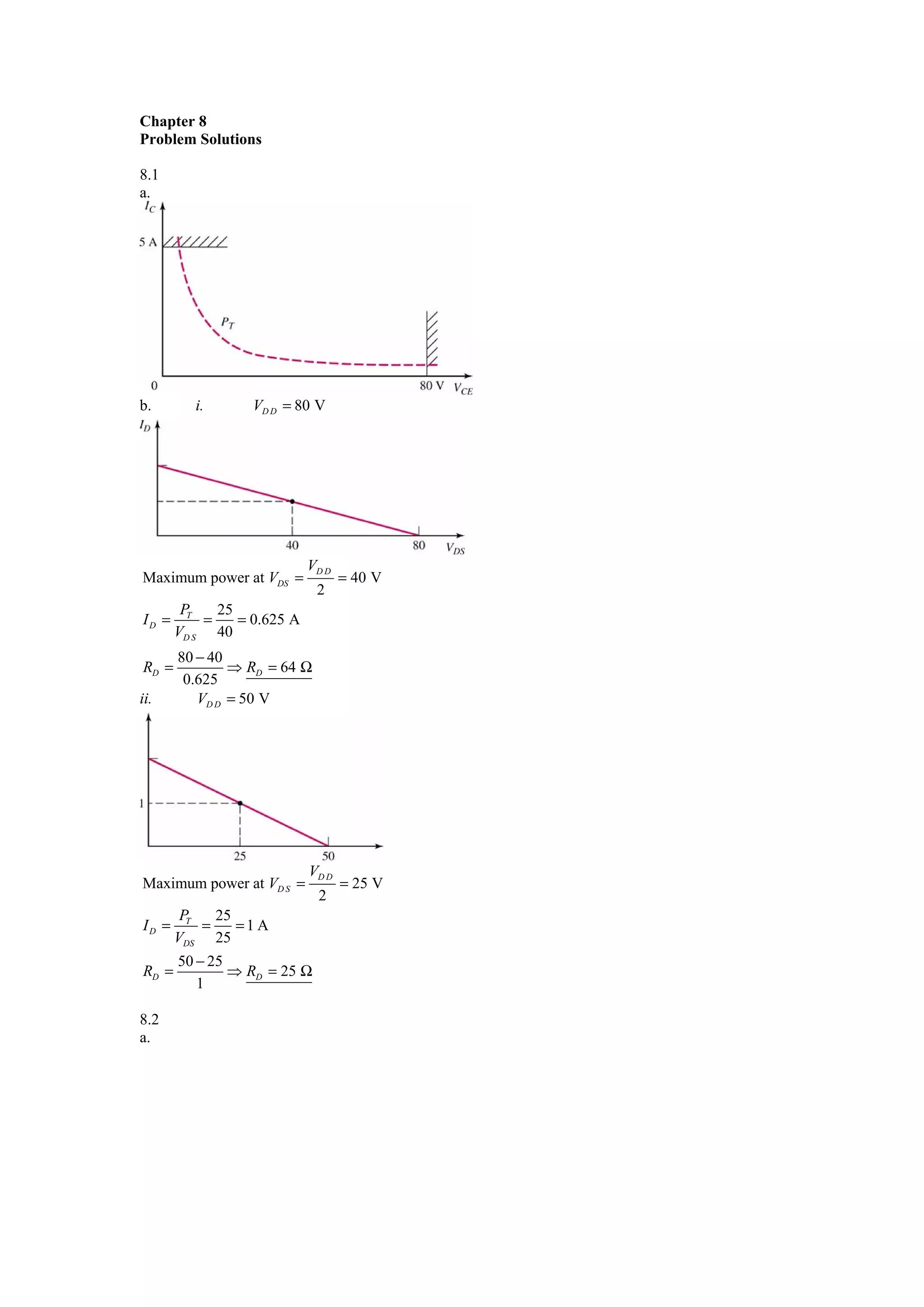
The document provides solutions to various problems involving the analysis and design of transistor amplifiers and power supplies. It examines concepts such as maximum power transfer, voltage gain, efficiency, heat dissipation, and voltage/current characteristics. Diagrams and calculations are presented to determine operating voltages and currents, power outputs, temperature rises, and efficiency for different circuit configurations under varying conditions.

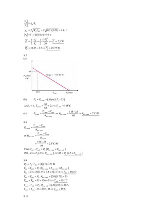
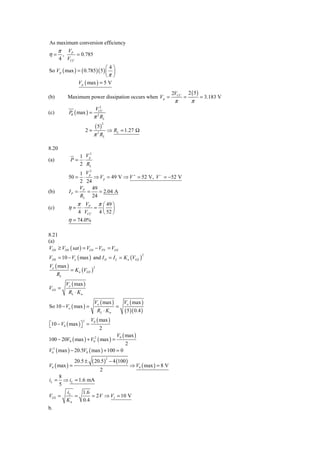
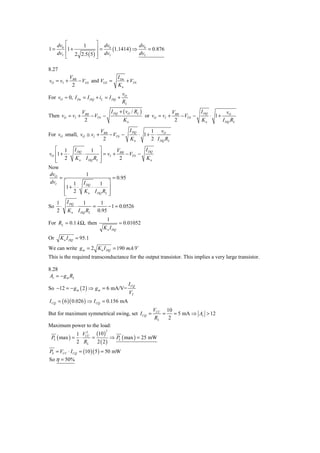
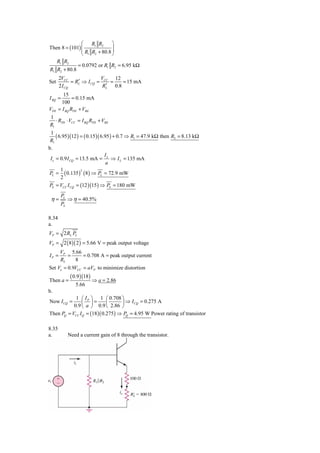
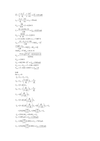
![Because of rπ 1 and Z, neglect effect of r0. Then neglecting r01, r02 and r03, we find
VX
I X = g m 3Vπ 3 + g m 2Vπ 2 + g m1Vπ 1 +
rπ 1 + Z
Now
⎛ r ⎞
Vπ 1 = ⎜ π 1 ⎟ VX , Vπ 2 ≅ g m1Vπ 1rπ 2
⎝ rπ 1 + Z ⎠
and
Vπ 3 = ( g m1Vπ 1 + g m 2Vπ 2 ) rπ 3
= ⎡ g m1Vπ 1 + g m 2 ( g m1Vπ 1rπ 2 ) ⎤ rπ 3
⎣ ⎦
⎛ r ⎞
Vπ 3 = ⎜ π 1 ⎟ [ g m1 + g m1 g m 2 rπ 2 ] rπ 3 ⋅ VX
⎝ rπ 1 + Z ⎠
( β + β1 β 2 ) rπ 3
Vπ 3 = 1 ⋅ VX
rπ 1 + Z
⎛ r ⎞ ⎛ βr ⎞
and Vπ 2 = g m1 ⎜ π 1 ⎟ rπ 2VX = ⎜ 1 π 2 ⎟ VX
⎝ rπ 1 + Z ⎠ ⎝ rπ 1 + Z ⎠
( β + β1 β 2 ) β 3 ββ β1 VX
Then I X = 1 ⋅ V X + 1 2 ⋅ VX + ⋅ VX +
rπ 1 + Z rπ 1 + Z rπ 1 + Z rπ 1 + Z
Then
VX rπ 1 + Z
R0 = =
I X 1 + β1 + β1 β 2 + ( β1 + β1 β 2 ) β 3
(10 )( 0.026 )
rπ 1 = = 0.169 MΩ
1.534
Z = 25 kΩ
Then
169 + 25
R0 =
1 + (10 ) + (10 )( 50 ) + ⎡10 + (10 )( 50 ) ⎤ ( 50 )
⎣ ⎦
194
R0 = = 0.00746 kΩ or Ro = 7.46 Ω
26, 011
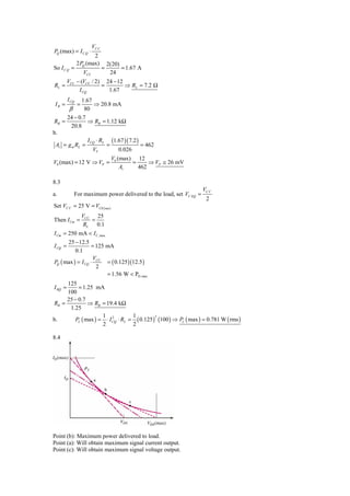
8.41
a Neglect base currents.
⎛I ⎞
VBB = 2VD = 2VT ln ⎜ Bias ⎟
⎝ IS ⎠
⎛ 5 × 10⁻³ ⎞
= 2 ( 0.026 ) ln ⎜ −13 ⎟
⇒ VBB = 1.281 V
⎝ 10 ⎠](https://image.slidesharecdn.com/ch08s-120608121902-phpapp01/85/Ch08s-21-320.jpg)
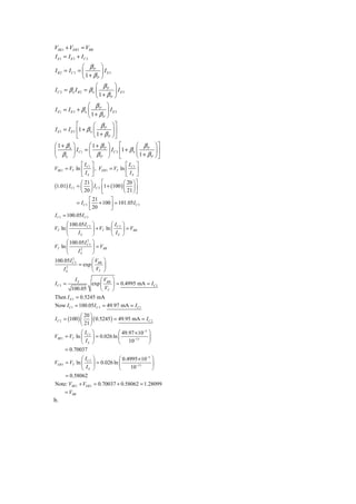
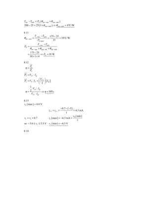
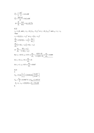
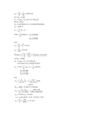
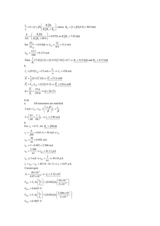
![10
v0 = 10 V ⇒ iE1 ≈ = 0.10 A = iC1
100
100
iB1 = = 1 mA
100
⎛ 4 × 10⁻³ ⎞
VBB = 2 ( 0.026 ) ln ⎜ −13 ⎟
= 1.2694 V
⎝ 10 ⎠
⎛ 0.1 ⎞
VBE1 = ( 0.026 ) ln ⎜ −13 ⎟ = 0.7184
⎝ 10 ⎠
VEB 3 = 1.2694 − 0.7184 = 0.55099 V
⎛ 0.55099 ⎞
I C 3 = 10−13 exp ⎜ ⎟ = 0.1598 mA
⎝ 0.026 ⎠
V 2 (10 )
2
PL = 0 = ⇒ PL = 1 W
RL 100
PQ1 = iC1 ⋅ vCE1 = ( 0.1)(12 − 10 ) ⇒ PQ1 = 0.2 W
PQ 3 = iC 3 ⋅ vEC 3 = ( 0.1598 ) (10 − [ 0.7 − 12]) ⇒ PQ 3 = 3.40 mW
iC 2 = (100 )( iC 3 ) = (100 )( 0.1598 ) = 15.98 mA
PQ 2 = iC 2 ⋅ vCE 2 = (15.98 ) (10 − [ −12]) ⇒ PQ 2 = 0.352 W
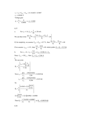
8.42
a.
⎛ 10 × 10−3 ⎞
VBB = 3 ( 0.026 ) ln ⎜ −12 ⎟
⇒ VBB = 1.74195 V
⎝ 2 × 10 ⎠
VBE1 + VBE 2 + VEB 3 = VBB
IC 2 IC 2
I C1 ≈ , IC 3 ≈
βn β n2
⎛I ⎞ ⎛I ⎞ ⎛I ⎞
VT ln ⎜ C1 ⎟ + VT ln ⎜ C 2 ⎟ + VT ln ⎜ C 3 ⎟ = VBB
⎝ IS ⎠ ⎝ IS ⎠ ⎝ IS ⎠
⎡ IC ⎤
3
VT ln ⎢ 3 2 3 ⎥ = VBB
⎣ βn IS ⎦
⎛V ⎞
I C 2 = β n I S 3 exp ⎜ BB ⎟
⎝ VT ⎠
⎛ 1.74195 ⎞
= ( 20 ) ( 20 × 10−12 ) 3 exp ⎜ ⎟
⎝ 0.026 ⎠
I C 2 = 0.20 A, I C1 ≈ 10 mA, I C 3 ≈ 0.5 mA
⎛ 10 × 10−3 ⎞
VBE1 = ( 0.026 ) ln ⎜ −12 ⎟
⇒ VBE1 = 0.58065 V
⎝ 2 × 10 ⎠
⎛ 0.2 ⎞
VBE 2 = ( 0.026 ) ln ⎜ −12 ⎟
⇒ VBE 2 = 0.6585 V
⎝ 2 × 10 ⎠
⎛ 0.5 × 10⁻³ ⎞
VEB 3 = ( 0.026 ) ln ⎜ −12 ⎟
⇒ VEB 3 = 0.50276 V
⎝ 2 × 10 ⎠
b.
1 V2 1 V2
PL = 10 W= ⋅ 0 = ⋅ 0 ⇒ V0 ( max ) = 20 V
2 RL 2 20
For v0 ( max ) :](https://image.slidesharecdn.com/ch08s-120608121902-phpapp01/85/Ch08s-23-320.jpg)


![[E book] introduction to electric circuits 6th ed [r. c. dorf and j. a. svoboda]](https://cdn.slidesharecdn.com/ss_thumbnails/ebookintroductiontoelectriccircuits6thedr-c-dorfandj-a-svoboda-100912170421-phpapp02-thumbnail.jpg?width=640&height=640&fit=bounds)