Downloaded 265 times
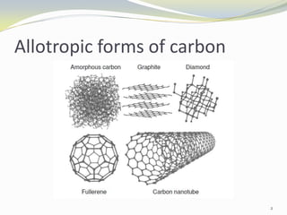
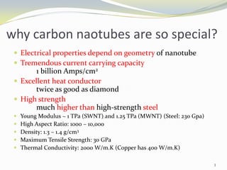
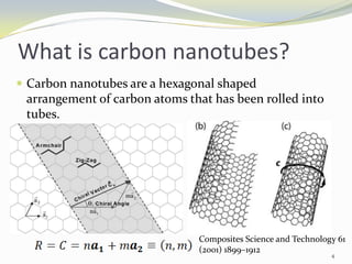
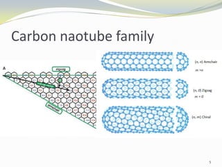
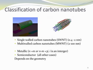
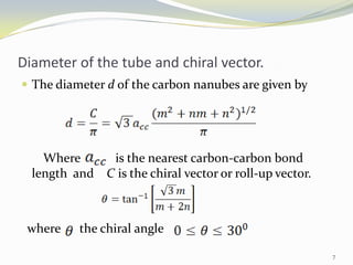


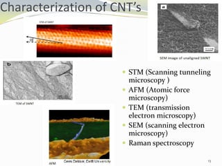
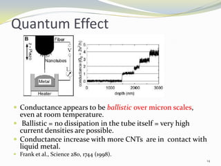

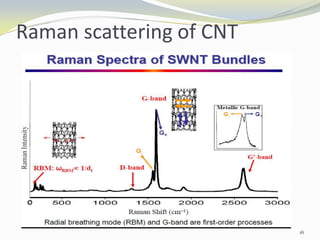
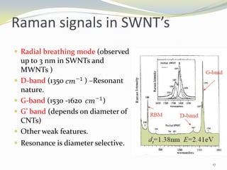


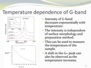
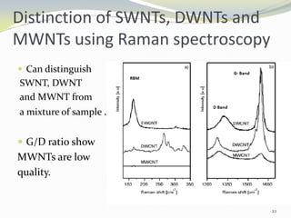
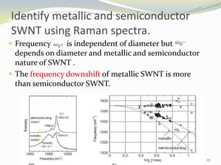
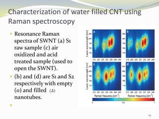

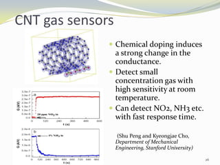
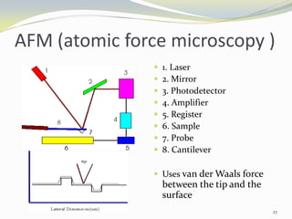


Carbon nanotubes have unique electrical, mechanical, and thermal properties that make them promising for a variety of applications. They have very high tensile strength and thermal conductivity. Their properties depend on their geometry, with single-walled nanotubes being metallic or semiconducting depending on their structure. Common synthesis methods include arc discharge, laser ablation, and chemical vapor deposition. Raman spectroscopy is useful for characterizing carbon nanotubes and can determine their diameter and identify defects. Potential applications of carbon nanotubes include use in electronics, gas sensors, field emission displays, and energy storage.


![Getting Started with Apache Spark: Big Data Made Simple [Free Meetup]](https://cdn.slidesharecdn.com/ss_thumbnails/apachesparkgettingstarted-260203175547-8361bcc3-thumbnail.jpg?width=640&height=640&fit=bounds)


