Downloaded 150 times
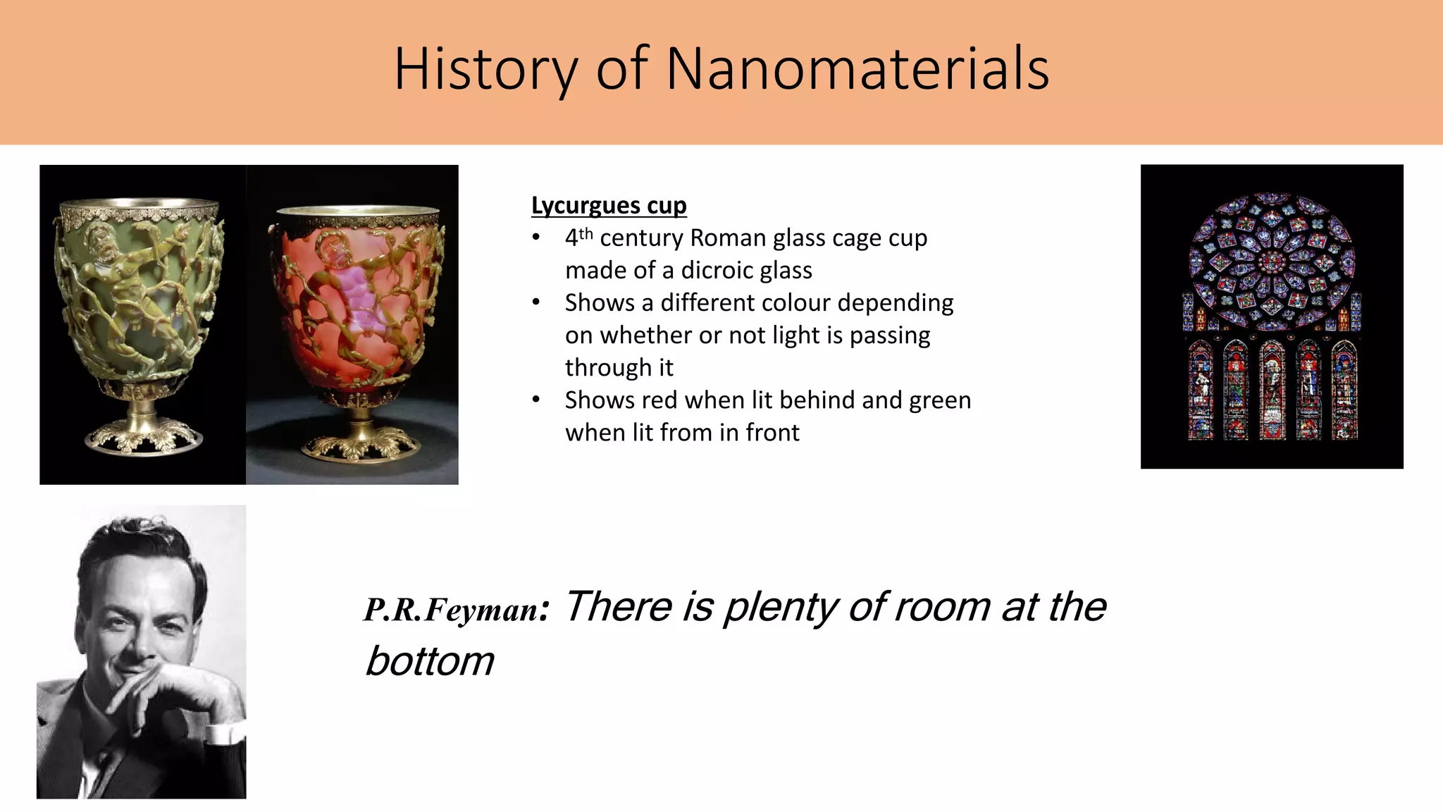
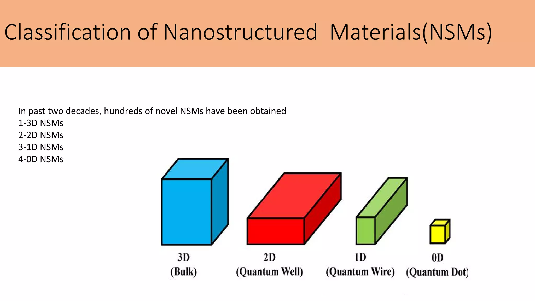
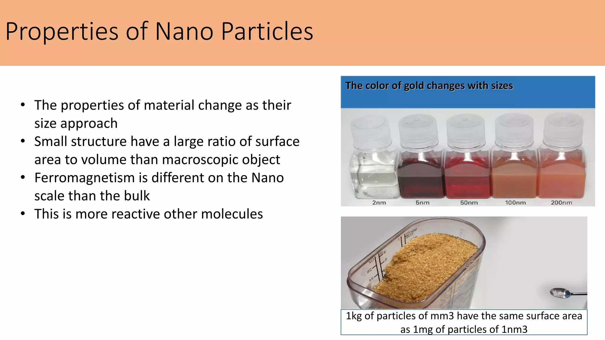
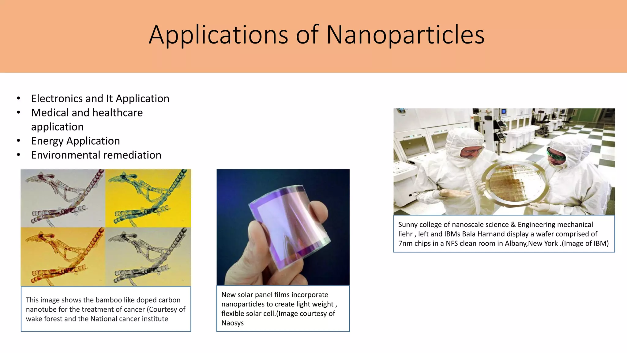
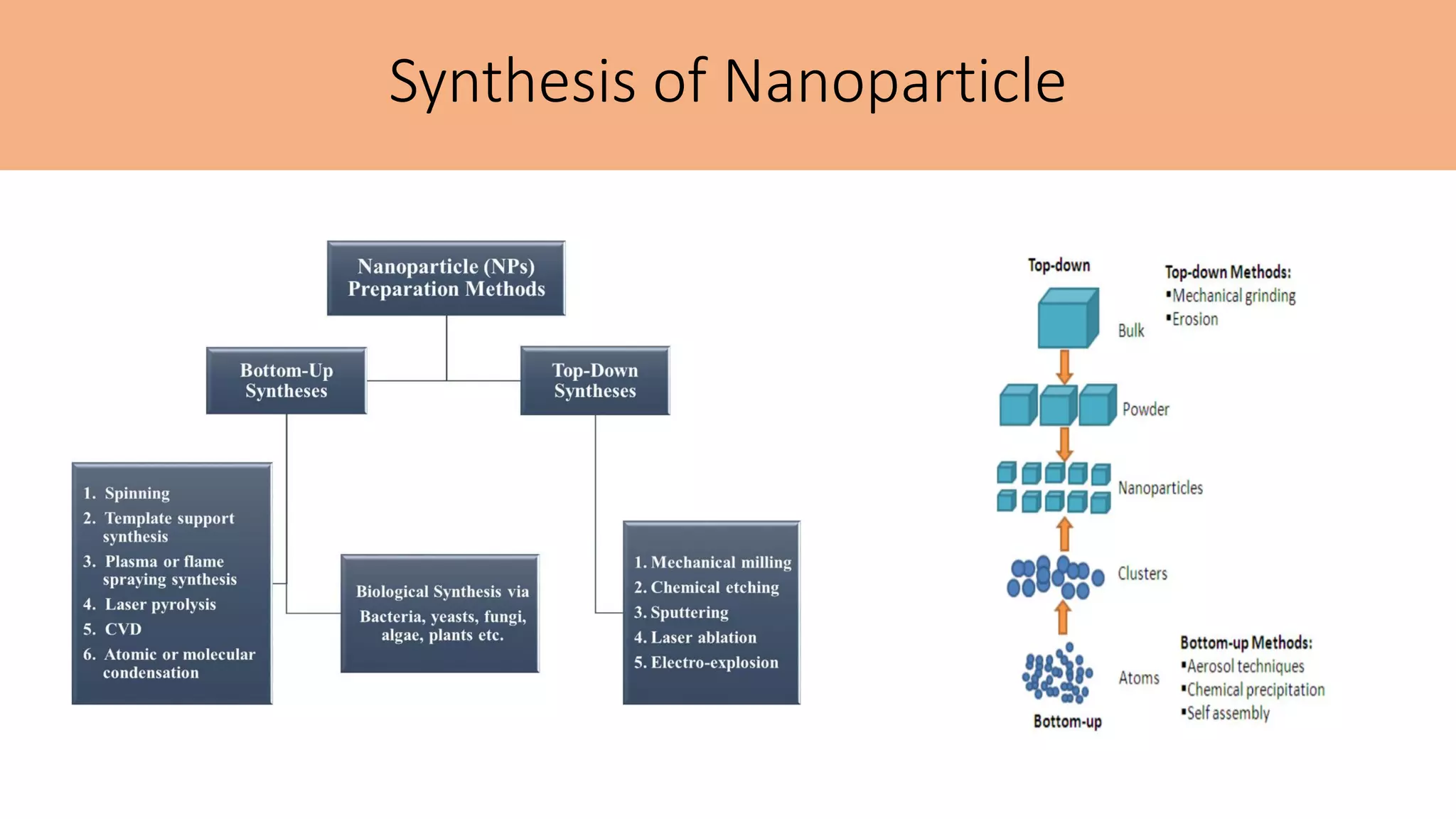

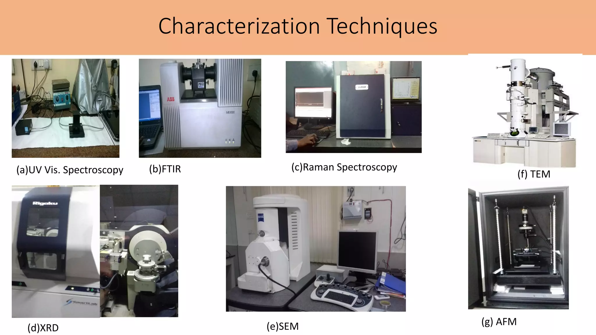
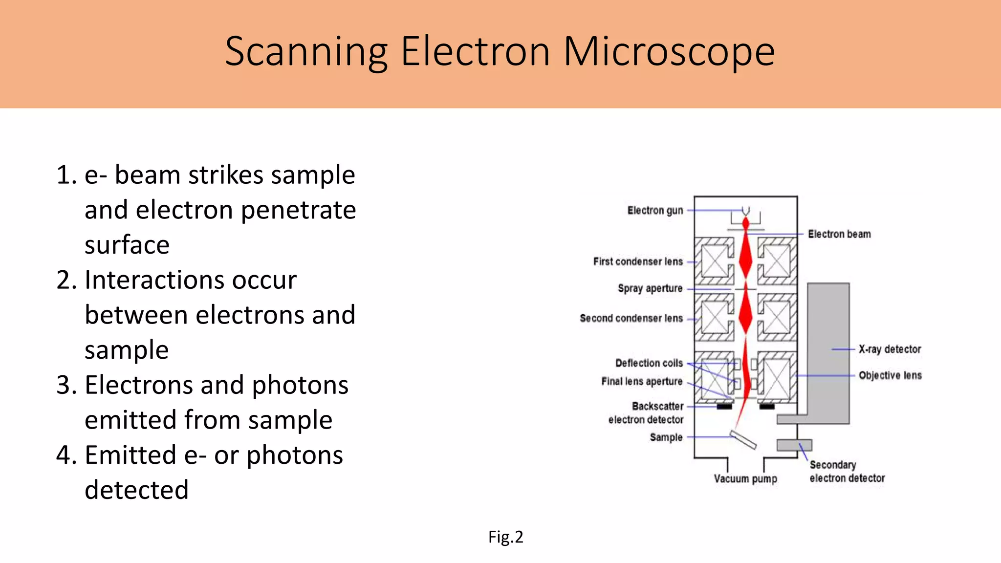
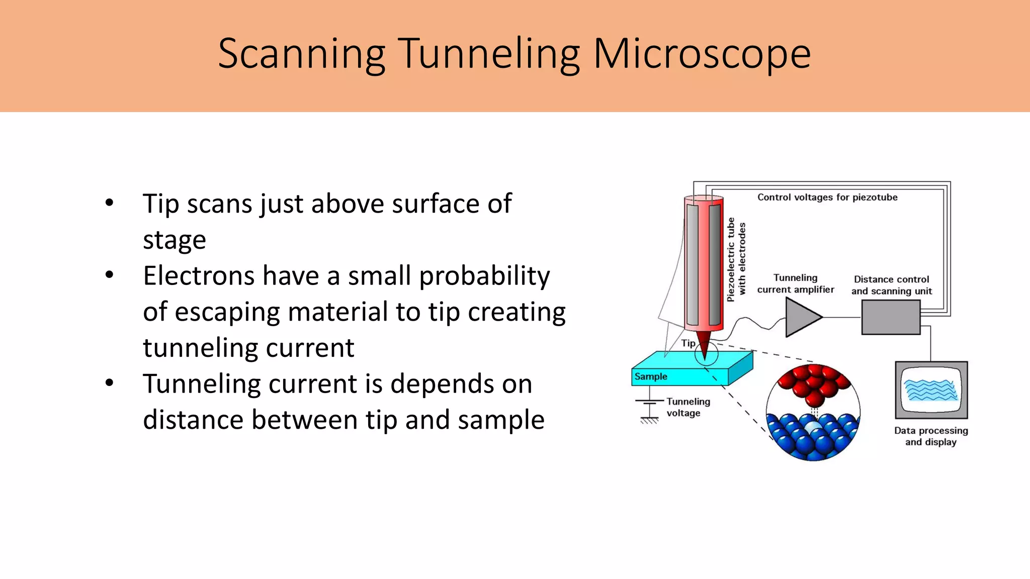
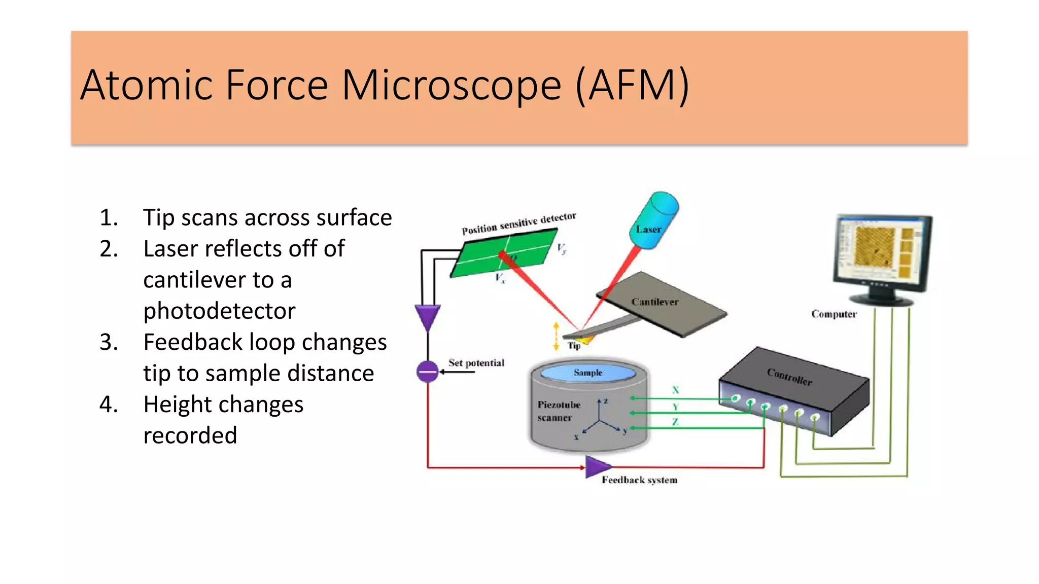

This document summarizes the history and applications of nanoparticles. It discusses early examples of nanomaterials like the Lycurgus Cup from the 4th century. It classifies nanostructured materials and describes how properties change at the nanoscale. Applications discussed include electronics, medicine, energy, and environmental remediation. Common synthesis methods are outlined as well as characterization techniques like UV-Vis spectroscopy, FTIR, XRD, SEM, TEM, and AFM. Scanning probe microscopes like SEM, STM, and AFM are also briefly described.


