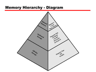
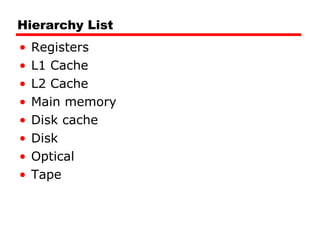
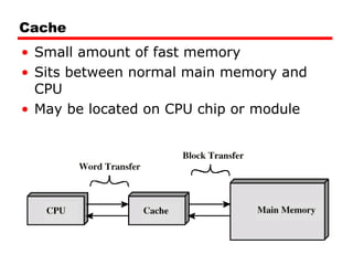
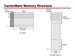
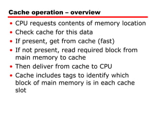
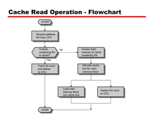
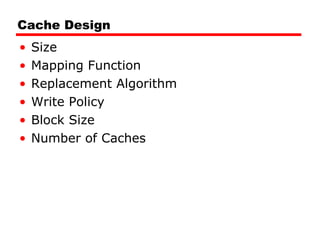
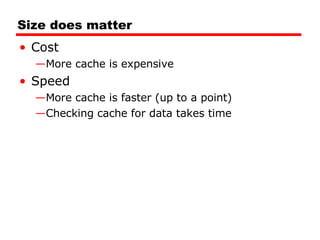
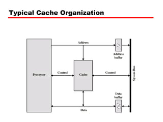
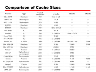
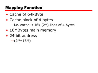
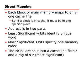
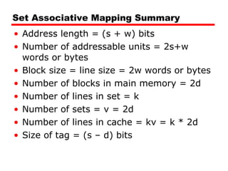
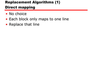
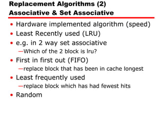
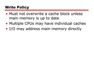
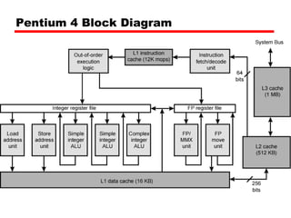
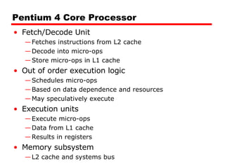
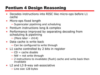
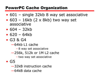
William Stallings  Computer Organization  and Architecture 7th Edition Chapter 4 Cache Memory
Characteristics Location Capacity Unit of transfer Access method Performance Physical type Physical characteristics Organisation
Location CPU Internal External
Capacity Word size The natural unit of organisation Number of words or Bytes
Unit of Transfer Internal Usually governed by data bus width External Usually a block which is much larger than a word Addressable unit Smallest location which can be uniquely addressed Word internally Cluster on M$ disks
Access Methods (1) Sequential Start at the beginning and read through in order Access time depends on location of data and previous location e.g. tape Direct Individual blocks have unique address Access is by jumping to vicinity plus sequential search Access time depends on location and previous location e.g. disk
Access Methods (2) Random Individual addresses identify locations exactly Access time is independent of location or previous access e.g. RAM Associative Data is located by a comparison with contents of a portion of the store Access time is independent of location or previous access e.g. cache
Memory Hierarchy Registers In CPU Internal or Main memory May include one or more levels of cache “ RAM” External memory Backing store
Memory Hierarchy - Diagram
Performance Access time Time between presenting the address and getting the valid data Memory Cycle time Time may be required for the memory to “recover” before next access Cycle time is access + recovery Transfer Rate Rate at which data can be moved
Physical Types Semiconductor RAM Magnetic Disk & Tape Optical CD & DVD Others Bubble Hologram
Physical Characteristics Decay Volatility Erasable Power consumption
Organisation Physical arrangement of bits into words Not always obvious e.g. interleaved
The Bottom Line How much? Capacity How fast? Time is money How expensive?
Hierarchy List Registers L1 Cache L2 Cache Main memory Disk cache Disk Optical Tape
So you want fast? It is possible to build a computer which uses only static RAM (see later) This would be very fast This would need no cache How can you cache cache? This would cost a very large amount
Locality of Reference During the course of the execution of a program, memory references tend to cluster e.g. loops
Cache Small amount of fast memory Sits between normal main memory and CPU May be located on CPU chip or module
Cache/Main Memory Structure
Cache operation – overview CPU requests contents of memory location Check cache for this data If present, get from cache (fast) If not present, read required block from main memory to cache Then deliver from cache to CPU Cache includes tags to identify which block of main memory is in each cache slot
Cache Read Operation - Flowchart
Cache Design Size Mapping Function Replacement Algorithm Write Policy Block Size Number of Caches
Size does matter Cost More cache is expensive Speed More cache is faster (up to a point) Checking cache for data takes time
Typical Cache Organization
Comparison of Cache Sizes     a  Two values seperated by a slash refer to instruction and data caches b  Both caches are instruction only; no data caches Processor Type Year of Introduction L1 cache a L2 cache L3 cache IBM 360/85 Mainframe 1968 16 to 32 KB — — PDP-11/70 Minicomputer 1975 1 KB — — VAX 11/780 Minicomputer 1978 16 KB — — IBM 3033 Mainframe 1978 64 KB — — IBM 3090 Mainframe 1985 128 to 256 KB — — Intel 80486 PC 1989 8 KB — — Pentium PC 1993 8 KB/8 KB 256 to 512 KB — PowerPC 601 PC 1993 32 KB — — PowerPC 620 PC 1996 32 KB/32 KB — — PowerPC G4 PC/server 1999 32 KB/32 KB 256 KB to 1 MB 2 MB IBM S/390 G4 Mainframe 1997 32 KB 256 KB 2 MB IBM S/390 G6 Mainframe 1999 256 KB 8 MB — Pentium 4 PC/server 2000 8 KB/8 KB 256 KB — IBM SP High-end server/ supercomputer 2000 64 KB/32 KB 8 MB — CRAY MTA b Supercomputer 2000 8 KB 2 MB — Itanium PC/server 2001 16 KB/16 KB 96 KB 4 MB SGI Origin 2001 High-end server 2001 32 KB/32 KB 4 MB — Itanium 2 PC/server 2002 32 KB 256 KB 6 MB IBM POWER5 High-end server 2003 64 KB 1.9 MB 36 MB CRAY XD-1 Supercomputer 2004 64 KB/64 KB 1MB —
Mapping Function Cache of 64kByte Cache block of 4 bytes i.e. cache is 16k (2 14 ) lines of 4 bytes 16MBytes main memory 24 bit address  (2 24 =16M)
Direct Mapping Each block of main memory maps to only one cache line i.e. if a block is in cache, it must be in one specific place Address is in two parts Least Significant w bits identify unique word Most Significant s bits specify one memory block The MSBs are split into a cache line field r and a tag of s-r (most significant)
Direct Mapping Address Structure 24 bit address 2 bit word identifier (4 byte block) 22 bit block identifier 8 bit tag (=22-14) 14 bit slot or line No two blocks in the same line have the same Tag field Check contents of cache by finding line and checking Tag Tag  s-r Line or Slot  r Word  w 8 14 2
Direct Mapping  Cache Line Table Cache line Main Memory blocks held 0 0, m, 2m, 3m…2s-m 1 1,m+1, 2m+1…2s-m+1 m-1 m-1, 2m-1,3m-1…2s-1
Direct Mapping Cache Organization
Direct Mapping  Example
Direct Mapping Summary Address length = (s + w) bits Number of addressable units = 2s+w words or bytes Block size = line size = 2w words or bytes Number of blocks in main memory = 2s+ w/2w = 2s Number of lines in cache = m = 2r Size of tag = (s – r) bits
Direct Mapping pros & cons Simple Inexpensive Fixed location for given block If a program accesses 2 blocks that map to the same line repeatedly, cache misses are very high
Associative Mapping A main memory block can load into any line of cache Memory address is interpreted as tag and word Tag uniquely identifies block of memory Every line’s tag is examined for a match Cache searching gets expensive
Fully Associative Cache Organization
Associative  Mapping Example
Associative Mapping Address Structure 22 bit tag stored with each 32 bit block of data Compare tag field with tag entry in cache to check for hit Least significant 2 bits of address identify which 16 bit word is required from 32 bit data block e.g. Address Tag Data Cache line FFFFFC FFFFFC 24682468 3FFF Tag  22 bit Word 2 bit
Associative Mapping Summary Address length = (s + w) bits Number of addressable units = 2s+w words or bytes Block size = line size = 2w words or bytes Number of blocks in main memory = 2s+ w/2w = 2s Number of lines in cache = undetermined Size of tag = s bits
Set Associative Mapping Cache is divided into a number of sets Each set contains a number of lines A given block maps to any line in a given set e.g. Block B can be in any line of set i e.g. 2 lines per set 2 way associative mapping A given block can be in one of 2 lines in only one set
Set Associative Mapping Example 13 bit set number Block number in main memory is modulo 2 13   000000, 00A000, 00B000, 00C000 … map to same set
Two Way Set Associative Cache Organization
Set Associative Mapping Address Structure Use set field to determine cache set to look in Compare tag field to see if we have a hit e.g Address Tag Data Set number 1FF 7FFC 1FF 12345678 1FFF 001 7FFC 001 11223344 1FFF Tag  9 bit Set  13 bit Word 2 bit
Two Way  Set  Associative  Mapping  Example
Set Associative Mapping Summary Address length = (s + w) bits Number of addressable units = 2s+w words or bytes Block size = line size = 2w words or bytes Number of blocks in main memory = 2d Number of lines in set = k Number of sets = v = 2d Number of lines in cache = kv = k * 2d Size of tag = (s – d) bits
Replacement Algorithms (1) Direct mapping No choice Each block only maps to one line Replace that line
Replacement Algorithms (2) Associative & Set Associative Hardware implemented algorithm (speed) Least Recently used (LRU) e.g. in 2 way set associative Which of the 2 block is lru? First in first out (FIFO) replace block that has been in cache longest Least frequently used replace block which has had fewest hits Random
Write Policy Must not overwrite a cache block unless main memory is up to date Multiple CPUs may have individual caches I/O may address main memory directly
Write through All writes go to main memory as well as cache Multiple CPUs can monitor main memory traffic to keep local (to CPU) cache up to date Lots of traffic Slows down writes Remember bogus write through caches!
Write back Updates initially made in cache only Update bit for cache slot is set when update occurs If block is to be replaced, write to main memory only if update bit is set Other caches get out of sync I/O must access main memory through cache N.B. 15% of memory references are writes
Pentium 4 Cache 80386 – no on chip cache 80486 – 8k using 16 byte lines and four way set associative organization Pentium (all versions) – two on chip L1 caches Data & instructions Pentium III – L3 cache added off chip Pentium 4 L1 caches 8k bytes 64 byte lines four way set associative L2 cache  Feeding both L1 caches 256k 128 byte lines 8 way set associative L3 cache on chip
Intel Cache Evolution Problem Solution Processor on which feature first appears External memory slower than the system bus. Add external cache using faster memory technology. 386 Increased processor speed results in external bus becoming a bottleneck for cache access. Move external cache on-chip, operating at the same speed as the processor. 486 Internal cache is rather small, due to limited space on chip Add external L2 cache using faster technology than main memory 486 Contention occurs when both the Instruction Prefetcher and the Execution Unit simultaneously require access to the cache. In that case, the Prefetcher is stalled while the Execution Unit’s data access takes place. Create separate data and instruction caches. Pentium Increased processor speed results in external bus becoming a bottleneck for L2 cache access. Create separate back-side bus that runs at higher speed than the main (front-side) external bus. The BSB is dedicated to the L2 cache. Pentium Pro Move L2 cache on to the processor chip. Pentium II Some applications deal with massive databases and must have rapid access to large amounts of data. The on-chip caches are too small. Add external L3 cache. Pentium III   Move L3 cache on-chip. Pentium 4
Pentium 4 Block Diagram
Pentium 4 Core Processor Fetch/Decode Unit Fetches instructions from L2 cache Decode into micro-ops Store micro-ops in L1 cache Out of order execution logic Schedules micro-ops Based on data dependence and resources May speculatively execute Execution units Execute micro-ops Data from L1 cache Results in registers Memory subsystem L2 cache and systems bus
Pentium 4 Design Reasoning Decodes instructions into RISC like micro-ops before L1 cache Micro-ops fixed length Superscalar pipelining and scheduling Pentium instructions long & complex Performance improved by separating decoding from scheduling & pipelining (More later – ch14) Data cache is write back Can be configured to write through L1 cache controlled by 2 bits in register CD = cache disable NW = not write through 2 instructions to invalidate (flush) cache and write back then invalidate L2 and L3 8-way set-associative  Line size 128 bytes
PowerPC Cache Organization 601 – single 32kb 8 way set associative 603 – 16kb (2 x 8kb) two way set associative 604 – 32kb 620 – 64kb G3 & G4 64kb L1 cache 8 way set associative 256k, 512k or 1M L2 cache two way set associative G5 32kB instruction cache 64kB data cache
PowerPC G5 Block Diagram
Internet Sources Manufacturer sites Intel IBM/Motorola Search on cache

04 Cache Memory

  • 1.
    William Stallings Computer Organization and Architecture 7th Edition Chapter 4 Cache Memory
  • 2.
    Characteristics Location CapacityUnit of transfer Access method Performance Physical type Physical characteristics Organisation
  • 3.
  • 4.
    Capacity Word sizeThe natural unit of organisation Number of words or Bytes
  • 5.
    Unit of TransferInternal Usually governed by data bus width External Usually a block which is much larger than a word Addressable unit Smallest location which can be uniquely addressed Word internally Cluster on M$ disks
  • 6.
    Access Methods (1)Sequential Start at the beginning and read through in order Access time depends on location of data and previous location e.g. tape Direct Individual blocks have unique address Access is by jumping to vicinity plus sequential search Access time depends on location and previous location e.g. disk
  • 7.
    Access Methods (2)Random Individual addresses identify locations exactly Access time is independent of location or previous access e.g. RAM Associative Data is located by a comparison with contents of a portion of the store Access time is independent of location or previous access e.g. cache
  • 8.
    Memory Hierarchy RegistersIn CPU Internal or Main memory May include one or more levels of cache “ RAM” External memory Backing store
  • 9.
  • 10.
    Performance Access timeTime between presenting the address and getting the valid data Memory Cycle time Time may be required for the memory to “recover” before next access Cycle time is access + recovery Transfer Rate Rate at which data can be moved
  • 11.
    Physical Types SemiconductorRAM Magnetic Disk & Tape Optical CD & DVD Others Bubble Hologram
  • 12.
    Physical Characteristics DecayVolatility Erasable Power consumption
  • 13.
    Organisation Physical arrangementof bits into words Not always obvious e.g. interleaved
  • 14.
    The Bottom LineHow much? Capacity How fast? Time is money How expensive?
  • 15.
    Hierarchy List RegistersL1 Cache L2 Cache Main memory Disk cache Disk Optical Tape
  • 16.
    So you wantfast? It is possible to build a computer which uses only static RAM (see later) This would be very fast This would need no cache How can you cache cache? This would cost a very large amount
  • 17.
    Locality of ReferenceDuring the course of the execution of a program, memory references tend to cluster e.g. loops
  • 18.
    Cache Small amountof fast memory Sits between normal main memory and CPU May be located on CPU chip or module
  • 19.
  • 20.
    Cache operation –overview CPU requests contents of memory location Check cache for this data If present, get from cache (fast) If not present, read required block from main memory to cache Then deliver from cache to CPU Cache includes tags to identify which block of main memory is in each cache slot
  • 21.
  • 22.
    Cache Design SizeMapping Function Replacement Algorithm Write Policy Block Size Number of Caches
  • 23.
    Size does matterCost More cache is expensive Speed More cache is faster (up to a point) Checking cache for data takes time
  • 24.
  • 25.
    Comparison of CacheSizes     a Two values seperated by a slash refer to instruction and data caches b Both caches are instruction only; no data caches Processor Type Year of Introduction L1 cache a L2 cache L3 cache IBM 360/85 Mainframe 1968 16 to 32 KB — — PDP-11/70 Minicomputer 1975 1 KB — — VAX 11/780 Minicomputer 1978 16 KB — — IBM 3033 Mainframe 1978 64 KB — — IBM 3090 Mainframe 1985 128 to 256 KB — — Intel 80486 PC 1989 8 KB — — Pentium PC 1993 8 KB/8 KB 256 to 512 KB — PowerPC 601 PC 1993 32 KB — — PowerPC 620 PC 1996 32 KB/32 KB — — PowerPC G4 PC/server 1999 32 KB/32 KB 256 KB to 1 MB 2 MB IBM S/390 G4 Mainframe 1997 32 KB 256 KB 2 MB IBM S/390 G6 Mainframe 1999 256 KB 8 MB — Pentium 4 PC/server 2000 8 KB/8 KB 256 KB — IBM SP High-end server/ supercomputer 2000 64 KB/32 KB 8 MB — CRAY MTA b Supercomputer 2000 8 KB 2 MB — Itanium PC/server 2001 16 KB/16 KB 96 KB 4 MB SGI Origin 2001 High-end server 2001 32 KB/32 KB 4 MB — Itanium 2 PC/server 2002 32 KB 256 KB 6 MB IBM POWER5 High-end server 2003 64 KB 1.9 MB 36 MB CRAY XD-1 Supercomputer 2004 64 KB/64 KB 1MB —
  • 26.
    Mapping Function Cacheof 64kByte Cache block of 4 bytes i.e. cache is 16k (2 14 ) lines of 4 bytes 16MBytes main memory 24 bit address (2 24 =16M)
  • 27.
    Direct Mapping Eachblock of main memory maps to only one cache line i.e. if a block is in cache, it must be in one specific place Address is in two parts Least Significant w bits identify unique word Most Significant s bits specify one memory block The MSBs are split into a cache line field r and a tag of s-r (most significant)
  • 28.
    Direct Mapping AddressStructure 24 bit address 2 bit word identifier (4 byte block) 22 bit block identifier 8 bit tag (=22-14) 14 bit slot or line No two blocks in the same line have the same Tag field Check contents of cache by finding line and checking Tag Tag s-r Line or Slot r Word w 8 14 2
  • 29.
    Direct Mapping Cache Line Table Cache line Main Memory blocks held 0 0, m, 2m, 3m…2s-m 1 1,m+1, 2m+1…2s-m+1 m-1 m-1, 2m-1,3m-1…2s-1
  • 30.
  • 31.
  • 32.
    Direct Mapping SummaryAddress length = (s + w) bits Number of addressable units = 2s+w words or bytes Block size = line size = 2w words or bytes Number of blocks in main memory = 2s+ w/2w = 2s Number of lines in cache = m = 2r Size of tag = (s – r) bits
  • 33.
    Direct Mapping pros& cons Simple Inexpensive Fixed location for given block If a program accesses 2 blocks that map to the same line repeatedly, cache misses are very high
  • 34.
    Associative Mapping Amain memory block can load into any line of cache Memory address is interpreted as tag and word Tag uniquely identifies block of memory Every line’s tag is examined for a match Cache searching gets expensive
  • 35.
  • 36.
  • 37.
    Associative Mapping AddressStructure 22 bit tag stored with each 32 bit block of data Compare tag field with tag entry in cache to check for hit Least significant 2 bits of address identify which 16 bit word is required from 32 bit data block e.g. Address Tag Data Cache line FFFFFC FFFFFC 24682468 3FFF Tag 22 bit Word 2 bit
  • 38.
    Associative Mapping SummaryAddress length = (s + w) bits Number of addressable units = 2s+w words or bytes Block size = line size = 2w words or bytes Number of blocks in main memory = 2s+ w/2w = 2s Number of lines in cache = undetermined Size of tag = s bits
  • 39.
    Set Associative MappingCache is divided into a number of sets Each set contains a number of lines A given block maps to any line in a given set e.g. Block B can be in any line of set i e.g. 2 lines per set 2 way associative mapping A given block can be in one of 2 lines in only one set
  • 40.
    Set Associative MappingExample 13 bit set number Block number in main memory is modulo 2 13 000000, 00A000, 00B000, 00C000 … map to same set
  • 41.
    Two Way SetAssociative Cache Organization
  • 42.
    Set Associative MappingAddress Structure Use set field to determine cache set to look in Compare tag field to see if we have a hit e.g Address Tag Data Set number 1FF 7FFC 1FF 12345678 1FFF 001 7FFC 001 11223344 1FFF Tag 9 bit Set 13 bit Word 2 bit
  • 43.
    Two Way Set Associative Mapping Example
  • 44.
    Set Associative MappingSummary Address length = (s + w) bits Number of addressable units = 2s+w words or bytes Block size = line size = 2w words or bytes Number of blocks in main memory = 2d Number of lines in set = k Number of sets = v = 2d Number of lines in cache = kv = k * 2d Size of tag = (s – d) bits
  • 45.
    Replacement Algorithms (1)Direct mapping No choice Each block only maps to one line Replace that line
  • 46.
    Replacement Algorithms (2)Associative & Set Associative Hardware implemented algorithm (speed) Least Recently used (LRU) e.g. in 2 way set associative Which of the 2 block is lru? First in first out (FIFO) replace block that has been in cache longest Least frequently used replace block which has had fewest hits Random
  • 47.
    Write Policy Mustnot overwrite a cache block unless main memory is up to date Multiple CPUs may have individual caches I/O may address main memory directly
  • 48.
    Write through Allwrites go to main memory as well as cache Multiple CPUs can monitor main memory traffic to keep local (to CPU) cache up to date Lots of traffic Slows down writes Remember bogus write through caches!
  • 49.
    Write back Updatesinitially made in cache only Update bit for cache slot is set when update occurs If block is to be replaced, write to main memory only if update bit is set Other caches get out of sync I/O must access main memory through cache N.B. 15% of memory references are writes
  • 50.
    Pentium 4 Cache80386 – no on chip cache 80486 – 8k using 16 byte lines and four way set associative organization Pentium (all versions) – two on chip L1 caches Data & instructions Pentium III – L3 cache added off chip Pentium 4 L1 caches 8k bytes 64 byte lines four way set associative L2 cache Feeding both L1 caches 256k 128 byte lines 8 way set associative L3 cache on chip
  • 51.
    Intel Cache EvolutionProblem Solution Processor on which feature first appears External memory slower than the system bus. Add external cache using faster memory technology. 386 Increased processor speed results in external bus becoming a bottleneck for cache access. Move external cache on-chip, operating at the same speed as the processor. 486 Internal cache is rather small, due to limited space on chip Add external L2 cache using faster technology than main memory 486 Contention occurs when both the Instruction Prefetcher and the Execution Unit simultaneously require access to the cache. In that case, the Prefetcher is stalled while the Execution Unit’s data access takes place. Create separate data and instruction caches. Pentium Increased processor speed results in external bus becoming a bottleneck for L2 cache access. Create separate back-side bus that runs at higher speed than the main (front-side) external bus. The BSB is dedicated to the L2 cache. Pentium Pro Move L2 cache on to the processor chip. Pentium II Some applications deal with massive databases and must have rapid access to large amounts of data. The on-chip caches are too small. Add external L3 cache. Pentium III   Move L3 cache on-chip. Pentium 4
  • 52.
  • 53.
    Pentium 4 CoreProcessor Fetch/Decode Unit Fetches instructions from L2 cache Decode into micro-ops Store micro-ops in L1 cache Out of order execution logic Schedules micro-ops Based on data dependence and resources May speculatively execute Execution units Execute micro-ops Data from L1 cache Results in registers Memory subsystem L2 cache and systems bus
  • 54.
    Pentium 4 DesignReasoning Decodes instructions into RISC like micro-ops before L1 cache Micro-ops fixed length Superscalar pipelining and scheduling Pentium instructions long & complex Performance improved by separating decoding from scheduling & pipelining (More later – ch14) Data cache is write back Can be configured to write through L1 cache controlled by 2 bits in register CD = cache disable NW = not write through 2 instructions to invalidate (flush) cache and write back then invalidate L2 and L3 8-way set-associative Line size 128 bytes
  • 55.
    PowerPC Cache Organization601 – single 32kb 8 way set associative 603 – 16kb (2 x 8kb) two way set associative 604 – 32kb 620 – 64kb G3 & G4 64kb L1 cache 8 way set associative 256k, 512k or 1M L2 cache two way set associative G5 32kB instruction cache 64kB data cache
  • 56.
  • 57.
    Internet Sources Manufacturersites Intel IBM/Motorola Search on cache