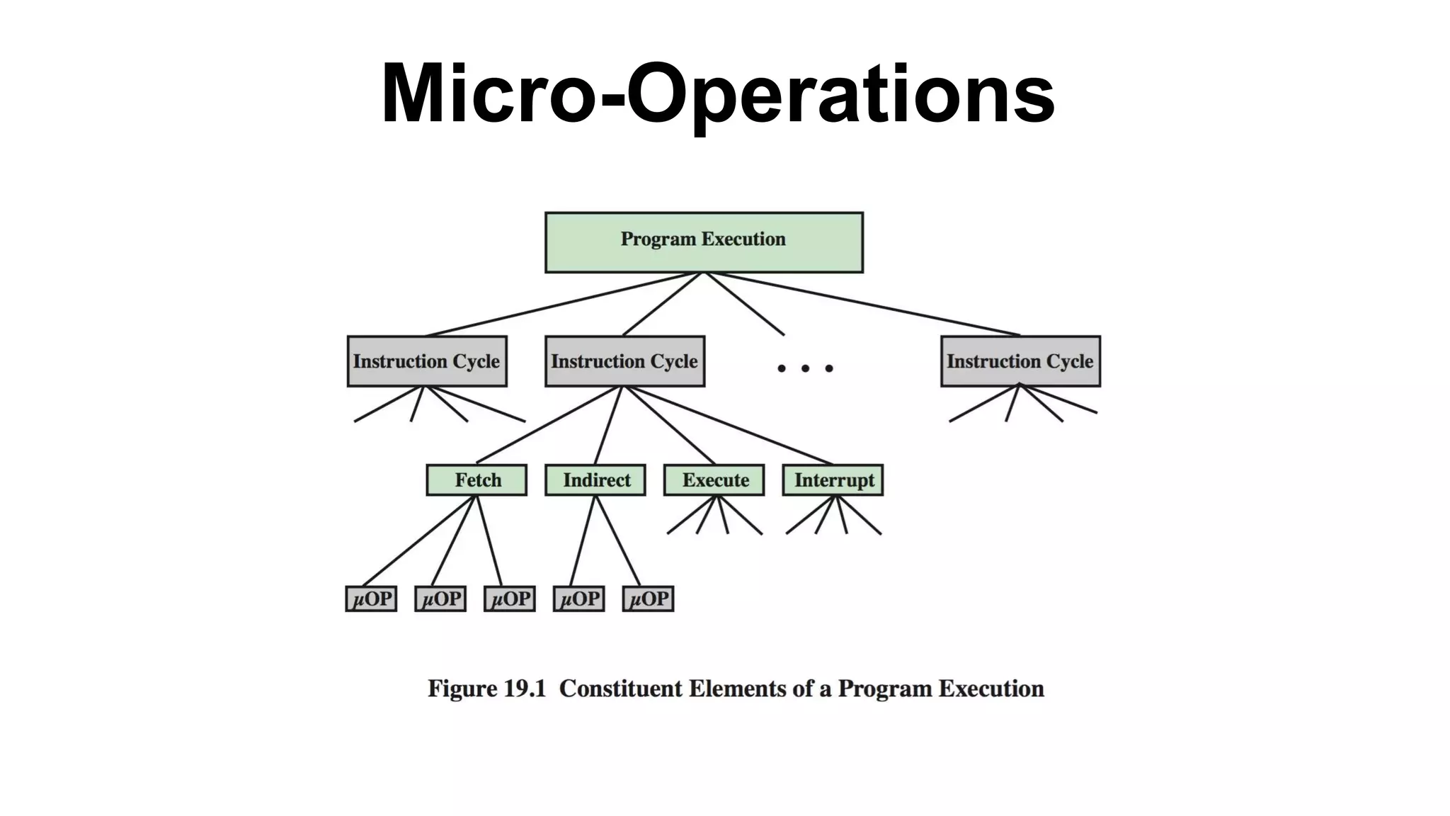
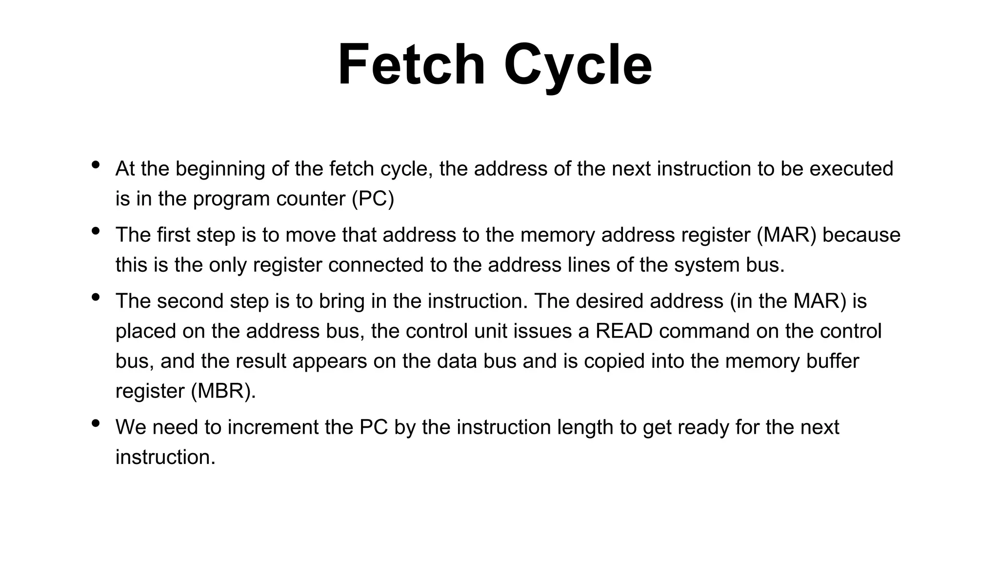
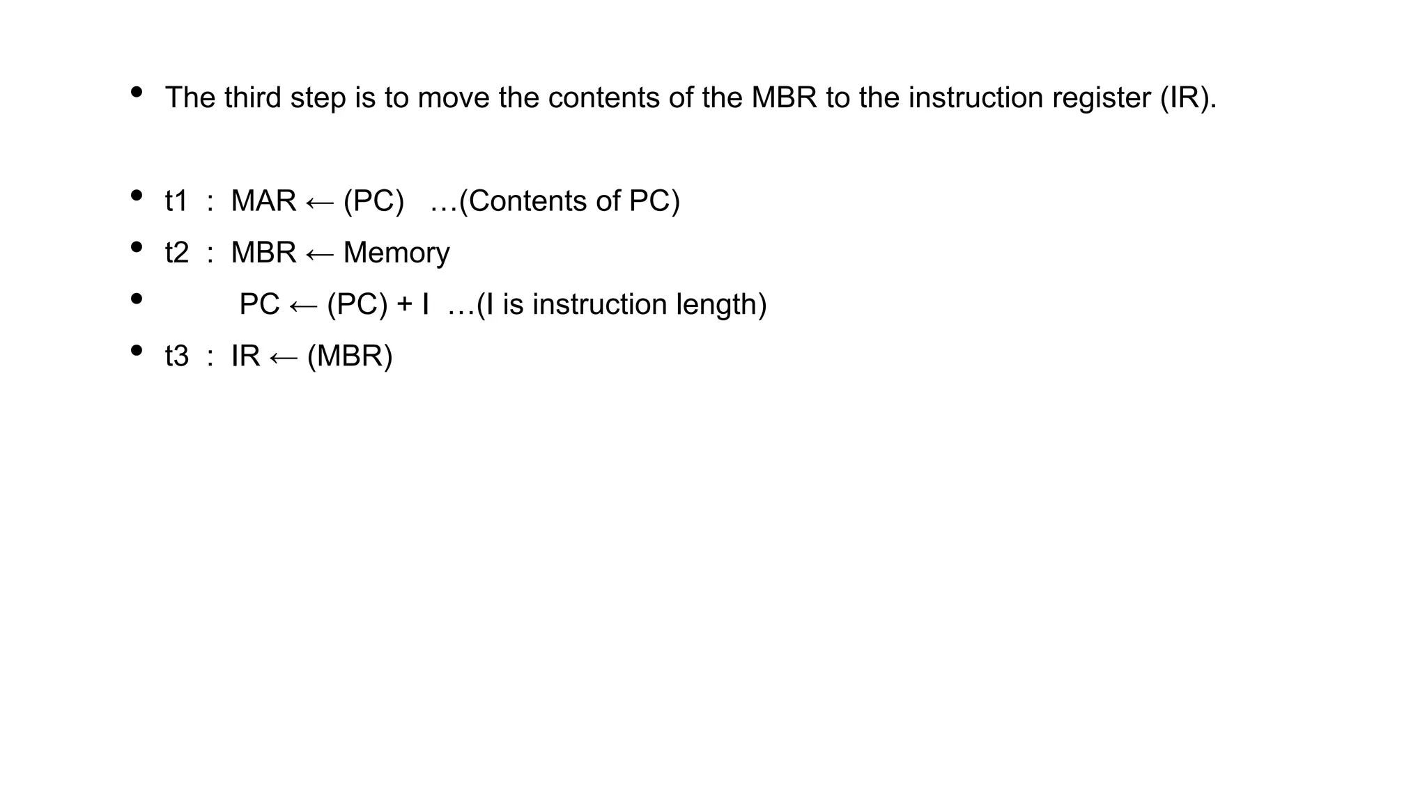
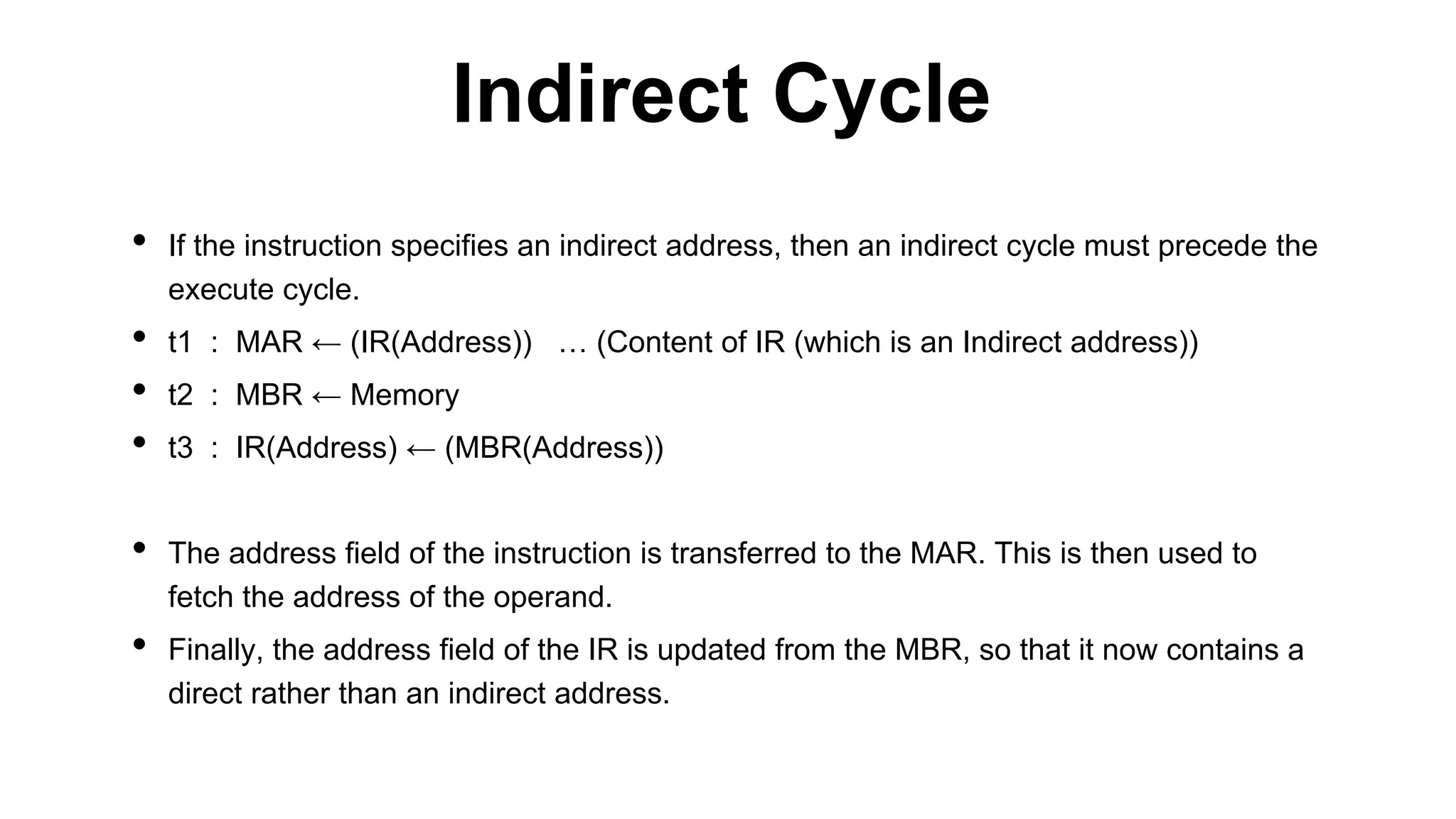
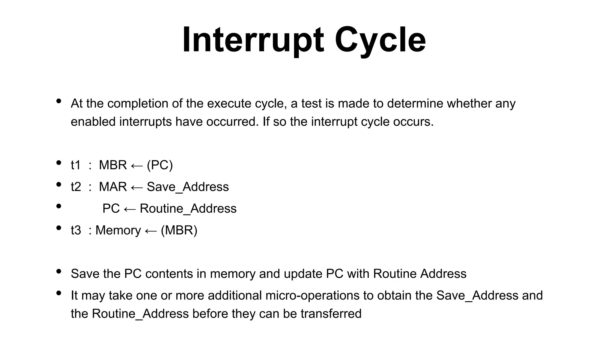
Micro operations
Fetch, Indirect, Interrupt, Execute, Instruction Cycle
Control Unit
Hardwired Control Unit
Microprogrammed Control Unit
Wilkie's Microprogrammed Control Unit
3. • At the beginning of the fetch cycle, the address of the next instruction to be executed
is in the program counter (PC)
• The first step is to move that address to the memory address register (MAR) because
this is the only register connected to the address lines of the system bus.
• The second step is to bring in the instruction. The desired address (in the MAR) is
placed on the address bus, the control unit issues a READ command on the control
bus, and the result appears on the data bus and is copied into the memory buffer
register (MBR).
• We need to increment the PC by the instruction length to get ready for the next
instruction.
Fetch Cycle
4. • The third step is to move the contents of the MBR to the instruction register (IR).
• t1 : MAR ← (PC) …(Contents of PC)
• t2 : MBR ← Memory
• PC ← (PC) + I …(I is instruction length)
• t3 : IR ← (MBR)
5. • If the instruction specifies an indirect address, then an indirect cycle must precede the
execute cycle.
• t1 : MAR ← (IR(Address)) … (Content of IR (which is an Indirect address))
• t2 : MBR ← Memory
• t3 : IR(Address) ← (MBR(Address))
• The address field of the instruction is transferred to the MAR. This is then used to
fetch the address of the operand.
• Finally, the address field of the IR is updated from the MBR, so that it now contains a
direct rather than an indirect address.
Indirect Cycle
6. • At the completion of the execute cycle, a test is made to determine whether any
enabled interrupts have occurred. If so the interrupt cycle occurs.
• t1 : MBR ← (PC)
• t2 : MAR ← Save_Address
• PC ← Routine_Address
• t3 : Memory ← (MBR)
• Save the PC contents in memory and update PC with Routine Address
• It may take one or more additional micro-operations to obtain the Save_Address and
the Routine_Address before they can be transferred
Interrupt Cycle
7. • Because of the variety opcodes, there are a number of different sequences of micro-
operations that can occur.
• The control unit examines the opcode and generates a sequence of micro-operations
based on the value of the opcode.
• This is referred to as instruction decoding.
• t1 : MAR ← (IR(address))
• t2 : MBR ← Memory
• t3 : R1 ← (R1) + (MBR)
Execute Cycle
8. • A 2-bit register called the instruction cycle code (ICC) designates the state of the
processor in terms of which portion of the cycle it is in:
• 00: Fetch
• 01: Indirect
• 10: Execute
• 11: Interrupt
• At the end of each of the four cycles, the ICC is set appropriately.
• The indirect cycle is always followed by the execute cycle.
• The interrupt cycle is always followed by the fetch cycle.
• For both the fetch and execute cycles, the next cycle depends on the state of the
system.
Instruction Cycle
9. • The basic functional elements of the processor are the following:
• ALU
• Registers
• Internal data paths
• External data paths
• Control unit
• Internal data paths are used to move data between registers and between register
and ALU. External data paths link registers to memory and I/O modules, often by
means of a system bus.
Control Unit
10. • All micro-operations fall into one of the following categories:
• Transfer data from one register to another.
• Transfer data from a register to an external interface (e.g., system
bus).
• Transfer data from an external interface to a register.
• Perform an arithmetic or logic operation, using registers for input and
output.
• For the control unit to perform its function, it must have inputs that allow it to determine
the state of the system and outputs that allow it to control the behavior of the system.
• Internally, the control unit must have the logic required to perform its sequencing and
execution functions.
11. • Control signals within the processor : Those that cause data to be moved from one
register to another, and those that activate specific ALU functions.
• Control signals to control bus : Control signals to memory, and control signals to the
I/O modules.
12. • In a hardwired implementation, the control unit is essentially a state machine circuit.
• Its input logic signals are transformed into a set of output logic signals, which are the
control signals.
Hardwired Control Unit
13. • The control unit makes use of the opcode and will perform different actions (issue a
different combination of control signals) for different instructions.
• To simplify the control unit logic, there should be a unique logic input for each opcode.
• This function can be performed by a decoder, which takes an encoded input and
produces a single output.
• The control unit emits different control signals at different time units within a single
instruction cycle.
• Thus, we would like a counter as input to the control unit, with a different control
signal being used for T1, T2, and so forth. At the end of an instruction cycle, the
control unit must feed back to the counter to reinitialize it at T1.
14. • To define the hardwired implementation of a control unit, all that remains is to discuss
the internal logic of the control unit that produces output control signals as a function
of its input signals.
• Essentially, what must be done is, for each control signal, to derive a Boolean
expression of that signal as a function of the inputs.
• PQ= 00 Fetch Cycle
• PQ= 01 Indirect Cycle
• PQ= 10 Execute Cycle
• PQ= 11 Interrupt Cycle
• At the end of each subcycle, the control unit must set the appropriate values of P and
Q to define the next subcycle to be performed.
15. • Advantages :
• They operate at very high speeds making it crucial for real time and other applications where time
is a major factor. Hardwired control units don’t need separate control memory for storage of
control word for generation of control signals. They perform the same task using logical circuitry
which is also the reason they are so fast.
• Hardwired control units are known to be more power efficient than their counterparts making them
an ideal choice for processors in mobile devices.
• Hardwired control units are now widely employed in RISC processors which are known for their
speed, reduced instruction set and support for limited addressing modes
• Disadvantages :
• To implement a control unit as an interconnection of basic logic elements is no easy task. The
design must include logic for sequencing through micro- operations, for executing micro-
operations, for interpreting opcodes, and for making decisions based on ALU flags. It is difficult to
design and test such a piece of hardware.
• Furthermore, the design is relatively inflexible. For example, it is difficult to change the design if
one wishes to add a new machine instruction.
16. • For microprogrammed control unit in addition to the use of control signals, each micro-
operation is described in symbolic notation.
• A set of micro- operations occurring at one time is known as a microinstruction
• Consider that for each micro-operation, all that the control unit is allowed to do is
generate a set of control signals.
• Thus, for any micro- operation, each control line emanating from the control unit is either
on or off.
• This condition can, of course, be represented by a binary digit for each control line. So we
could construct a control word in which each bit represents one control line.
• Then each micro-operation would be represented by a different pattern of 1s and 0s in the
control word.
Micro-Programmed Control Unit
17. • Suppose we string together a sequence of control words to represent the sequence of
micro-operations performed by the control unit.
• Sometimes we have an indirect cycle ; sometimes we do not. So let us put our control
words in a memory, with each word having a unique address.
• Now add an address field to each control word, indicating the location of the next
control word to be executed if a certain condition is true. Also, add a few bits to
specify the condition.
18.
19. • The control memory of is a concise description of the complete operation of the
control unit.
• It defines the sequence of micro- operations to be performed during each cycle (fetch,
indirect, execute, interrupt), and it specifies the sequencing of these cycles.
• The microinstructions in each routine are to be executed sequentially.
• Each routine ends with a branch or jump instruction indicating where to go next.
(Whether to the next consecutive instruction or take a branch)
• There is a special execute cycle routine whose only purpose is to signify that one of
the machine instruction routines (AND, ADD, and so on) is to be executed next,
depending on the current opcode.
20.
21. • The control memory of contains a program that describes the behavior of the control
unit.
• It follows that we could implement the control unit by simply executing that program.
• The set of microinstructions is stored in the control memory.
• The control address register contains the address of the next microinstruction to be
read.
• When a microinstruction is read from the control memory, it is transferred to a control
buffer register.
• The left-hand portion of that register connects to the control lines emanating from the
control unit. Thus, reading a microinstruction from the control memory is the same as
executing that microinstruction.
• Sequencing unit loads the control address register and issues a read command.
22. • To execute an instruction, the sequencing logic unit issues a READ command to the control
memory.
• The word whose address is specified in the control address register is read into the control buffer
register.
• The content of the control buffer register generates control signals (left part) and next-address
information for the sequencing logic unit (right part).
• The sequencing logic unit loads a new address into the control address register based on the
next-address information from the control buffer register and the ALU flags.
• All this happens during one clock pulse.
Functioning Microprogrammed CU
23. • The last step just listed needs elaboration. At the conclusion of each microinstruction,
the sequencing logic unit loads a new address into the control address register.
• Depending on the value of the ALU flags and the control buffer register, one of three
decisions is made :
• Get the next instruction : Add 1 to the control address register.
• Jump to a new routine based on a jump microinstruction : Load the address field of
the control buffer register into the control address register.
• Jump to a machine instruction routine : Load the control address register based on
the opcode in the IR.
• The upper decoder translates the opcode of the IR into a control memory address.
24. • The principal advantage of the use of microprogramming to implement a control unit is
that it simplifies the design of the control unit.
• Thus, it is both cheaper and less error prone to implement.
• A hardwired control unit must contain complex logic for sequencing through the many
micro-operations of the instruction cycle. On the other hand, the decoders and
sequencing logic unit of a microprogrammed control unit are very simple pieces of
logic.
• The principal disadvantage of a microprogrammed unit is that it will be somewhat
slower than a hardwired unit of comparable technology. Despite this,
microprogramming is the dominant technique for implementing control units in pure
CISC architectures, due to its ease of implementation.
Advantages and Disadvantages
26. • During a machine cycle, one row of the matrix is activated with a pulse. This
generates signals at those points where a diode is present (indicated by a dot in the
diagram).
• Each row of the matrix is one microinstruction, and the layout of the matrix is the
control memory.
• At the beginning of the cycle, the address of the row to be pulsed is contained in
Register I.
• The decoder, when activated by a clock pulse, activates one row of the matrix.
• Depending on the control signals, either the opcode in the instruction register or the
second part of the pulsed row is passed into Register II during the cycle.
27. • Register II is then gated to Register I by a clock pulse.
• Alternating clock pulses are used to activate a row of the matrix and to transfer from
Register II to Register I.
• The two-register arrangement is needed because the decoder is simply a
combinatorial circuit; with only one register, the output would become the input during
a cycle, causing an unstable condition.