Downloaded 74 times
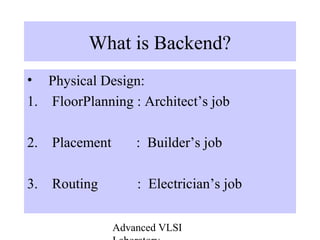
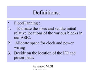
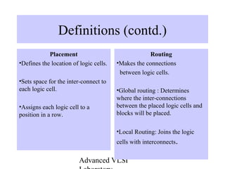
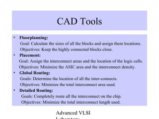
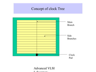
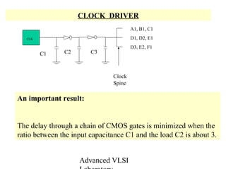
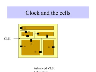
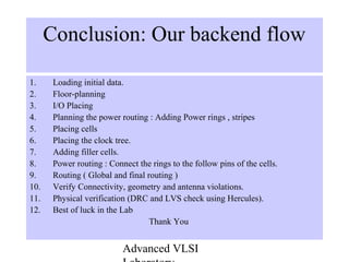

The document discusses the backend design flow in VLSI, including floorplanning, placement, and routing. Floorplanning involves estimating block sizes and locations. Placement defines the location of logic cells and interconnect space. Routing connects the placed logic cells, with global routing determining interconnect locations and local routing connecting cells. The document outlines the goals and objectives of EDA tools for floorplanning, placement, and routing. It also discusses clock trees, placement strategies, and concludes with the overall backend flow.