Download to read offline
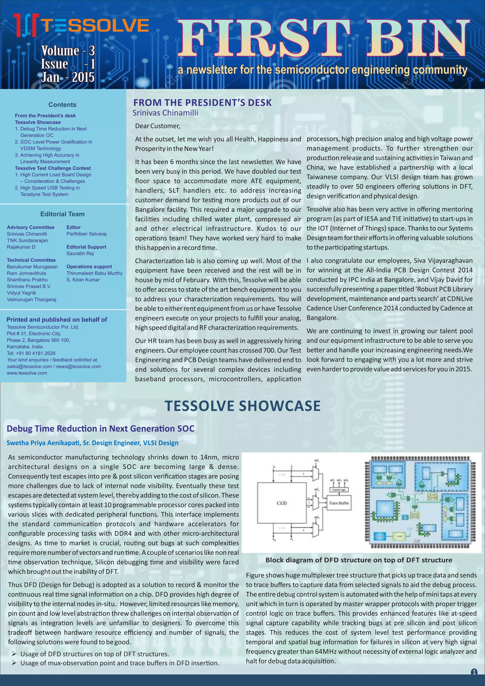

This document is the January 2015 newsletter for Tessolve Semiconductor Pvt. Ltd. It contains the following: 1. A message from the President's desk welcoming the new year and providing an update on the company's growth, including doubling their test floor space, upcoming characterization lab, hiring more engineers, and establishing partnerships. 2. Two articles in the "Tessolve Showcase" section about reducing debug time in next generation SOCs using DFD structures on DFT and achieving high accuracy in linearity measurement. 3. An article on SOC level power gratification in VDSM technology and the various power grid methodologies used.


![Design for Test [DFT]-1 (1).pdf DESIGN DFT](https://cdn.slidesharecdn.com/ss_thumbnails/designfortestdft-11-231227151941-28a508a3-thumbnail.jpg?width=640&height=640&fit=bounds)