This document provides an overview of signal integrity (SI) and discusses various SI topics including transmission line theory, time domain analysis, frequency domain analysis, equalization techniques, and high speed interfaces. It begins with defining SI and its importance. It then covers transmission line theory concepts such as lossy and lossless lines, single-ended and differential signaling. The document discusses time domain analysis methods like eye patterns, jitter, setup/hold times and rise/fall times. Frequency domain analysis methods such as S-parameters, insertion loss, return loss, and crosstalk are also outlined. Finally, it briefly introduces some common high speed interfaces including DDR, SAS, SATA, USB, and PCIe.
In this document
Powered by AI
Introduction to Signal Integrity (SI) ensuring quality of electrical signals to prevent interference.
Exploration of Transmission Line Theory including Lossy/Lossless types and signaling methods.
Comparison of Time vs. Frequency Domain Analysis; advantages in analyzing signal behavior.
Detailed examination of time-domain concepts including jitter, rise/fall times, and setup/hold times.
Introduction to frequency domain analysis; S-parameters, insertion and return loss are discussed.
Definition and implications of crosstalk in transmission lines; includes near-end and far-end crosstalk.
Definitions of Nyquist Rate and Knee Frequency relevant to sampling and signal integrity.
Overview of high-speed interface standards: DDR, SAS, SATA, detailing their evolution and specifications.
Description of USB technology including versions and specifications for modern electronic devices.
Diverse equalization techniques like FFE, DFE, and CTLE for enhancing signal quality.
Introduction to various 3D modeling methods like MOM, FEM and FDTD for analyzing electromagnetic fields.
Design of Experiments (DOE), Genetic Algorithms (GA) and Artificial Neural Networks (ANN) as optimization tools.
Overview of HFSS solution types for simulating structures focusing on signal integrity for high-frequency designs.
Outline
Overview ofSI
Transmission Line Theory
Time Domain Analysis
Frequency Domain Analysis
Equalization Techniques
High Speed interfaces
3D Modeling
3.
Overview
Signal integrityis an important activity at all levels of
electronics packaging and assembly, from internal
connections of an integrated circuit (IC),through
the package, the printed circuit board (PCB),
the backplane.
SI is a set of measures of the quality of an electrical
signal.
That ensures all signals transmitted are received
correctly.
That ensures signals don’t interfere with one another.
That ensures signal don’t damage any device.
4.
Transmission line Theory
Introduction
Lossy Transmission Line
Lossless Transmission Line
Single Ended Signaling
Differential Signaling
Tightly Coupled & Loosely Coupled
5.
Introduction
The transferof energy from one point to another takes
through either wave guides or transmission lines.
In an electronic system, the delivery of power
requires the connection of two wires between the
source and the load. At low frequencies, power is
considered to be delivered to the load through the
wire.
In the microwave frequency region, power is
considered to be in electric and magnetic fields that
are guided from lace to place by some physical
structure. Any physical structure that will guide an
electromagnetic wave place to place is called a
Transmission Line.
6.
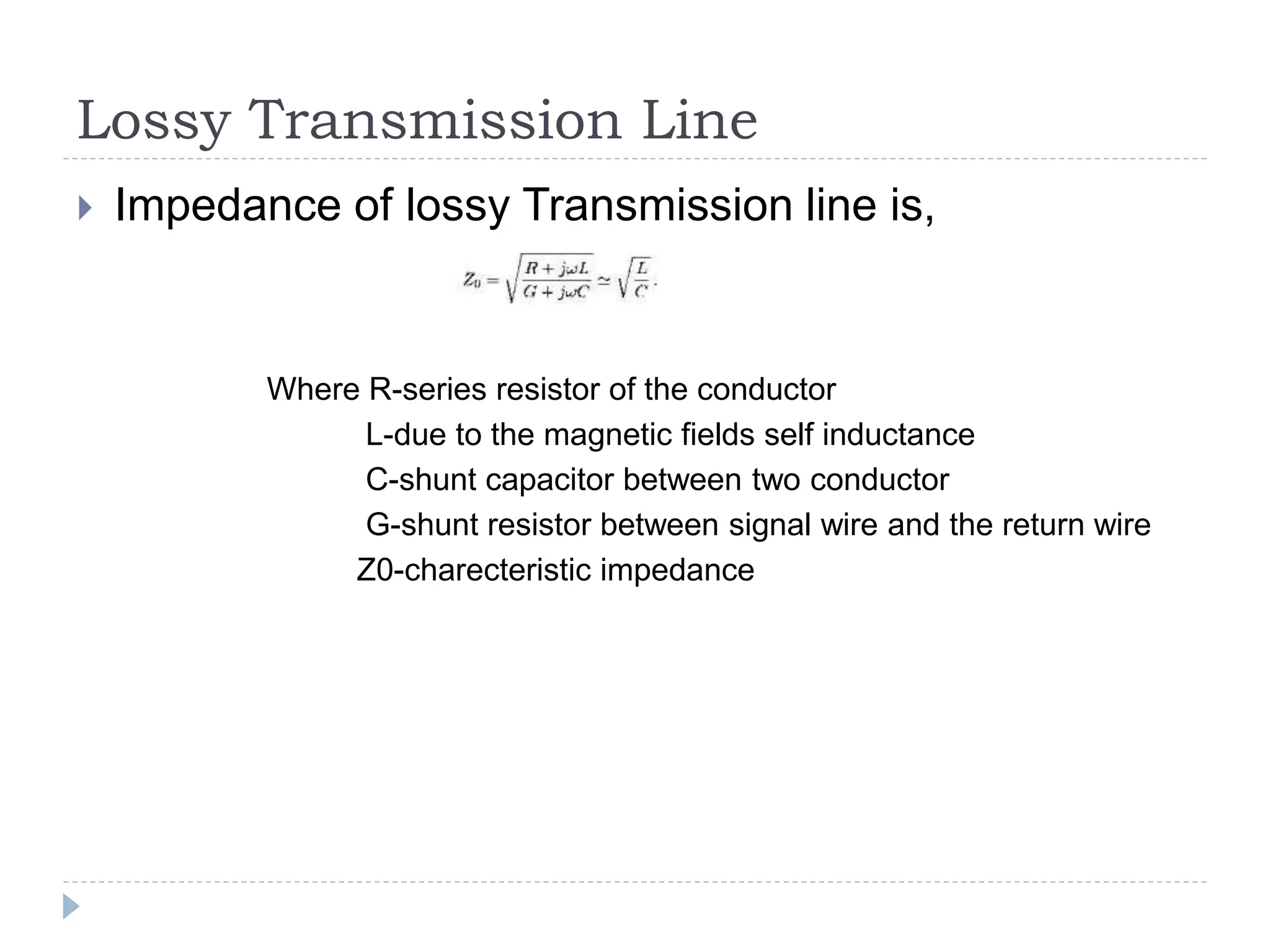
Lossy Transmission Line
Impedance of lossy Transmission line is,
Where R-series resistor of the conductor
L-due to the magnetic fields self inductance
C-shunt capacitor between two conductor
G-shunt resistor between signal wire and the return wire
Z0-charecteristic impedance
7.
Lossless Transmission Line
Impedance of lossless Transmission line is,
When the R and G are negligibly small the
transmission line,the model depends only on the L
and C elements
8.
Single Ended Signaling
A single-ended measurement is taken as the voltage
difference between a wire and ground.
The noise is only on the positive wire, and as a
result, it is still measured along with the output
voltage from the sensor
Single-ended signaling is the simplest and most
commonly used method of transmitting electrical
signals over wires.
One wire carries a varying volt that represents the
signal, while the other wire is connected to a
reference voltage, usually gnd.
9.
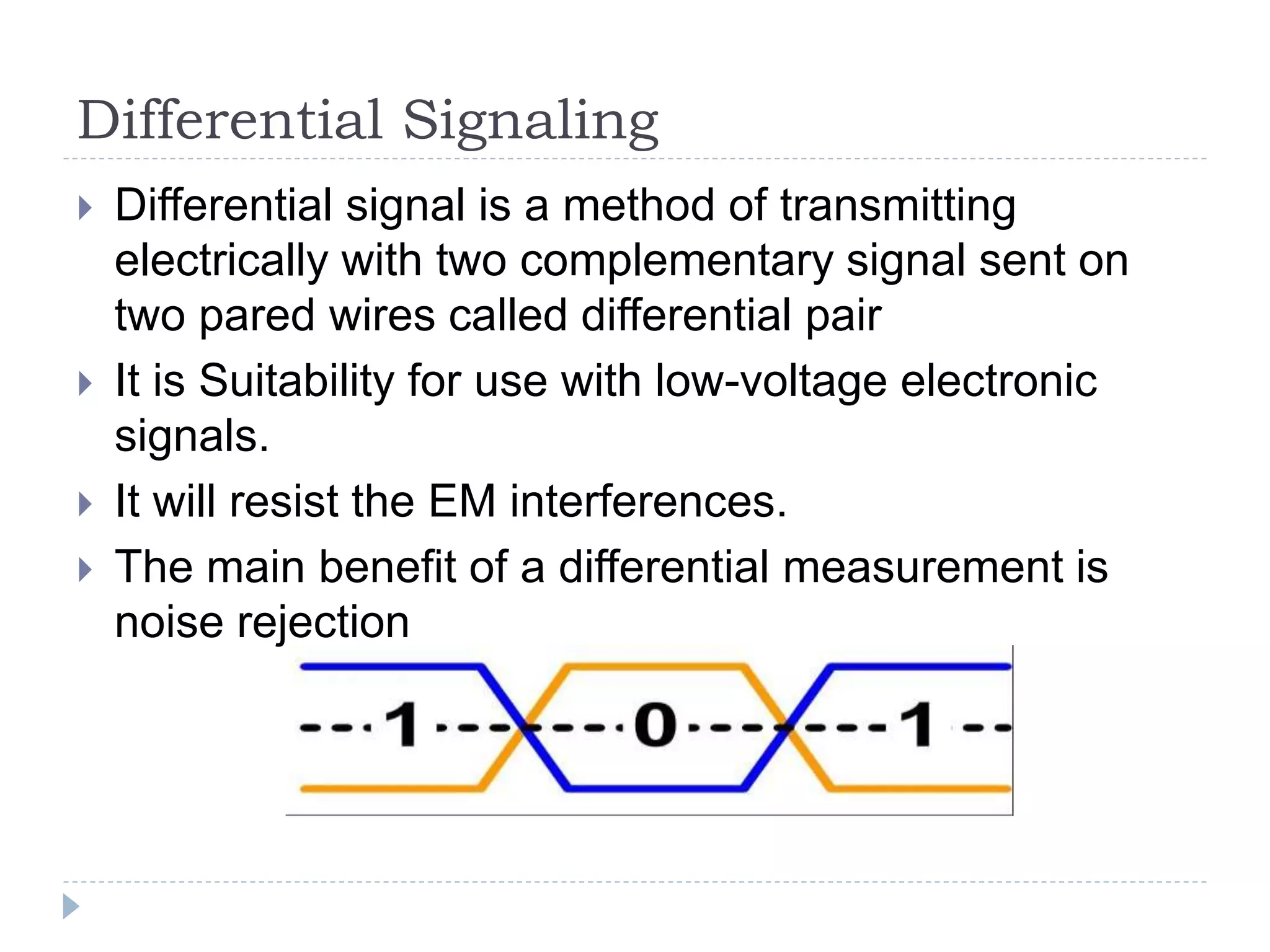
Differential Signaling
Differentialsignal is a method of transmitting
electrically with two complementary signal sent on
two pared wires called differential pair
It is Suitability for use with low-voltage electronic
signals.
It will resist the EM interferences.
The main benefit of a differential measurement is
noise rejection
10.
Tight coupling &Looselycoupled
Tight coupling is usually reduces flexibility and re-usability A Tightly
Coupled Object is an object that needs to know quite a bit about
other objects and are usually highly dependent on each other's
interfaces.
Loosely coupled to reduce the inter-dependencies between
components of a system Loose coupling is a much more generic
concept intended to increase the flexibility of a system
11.
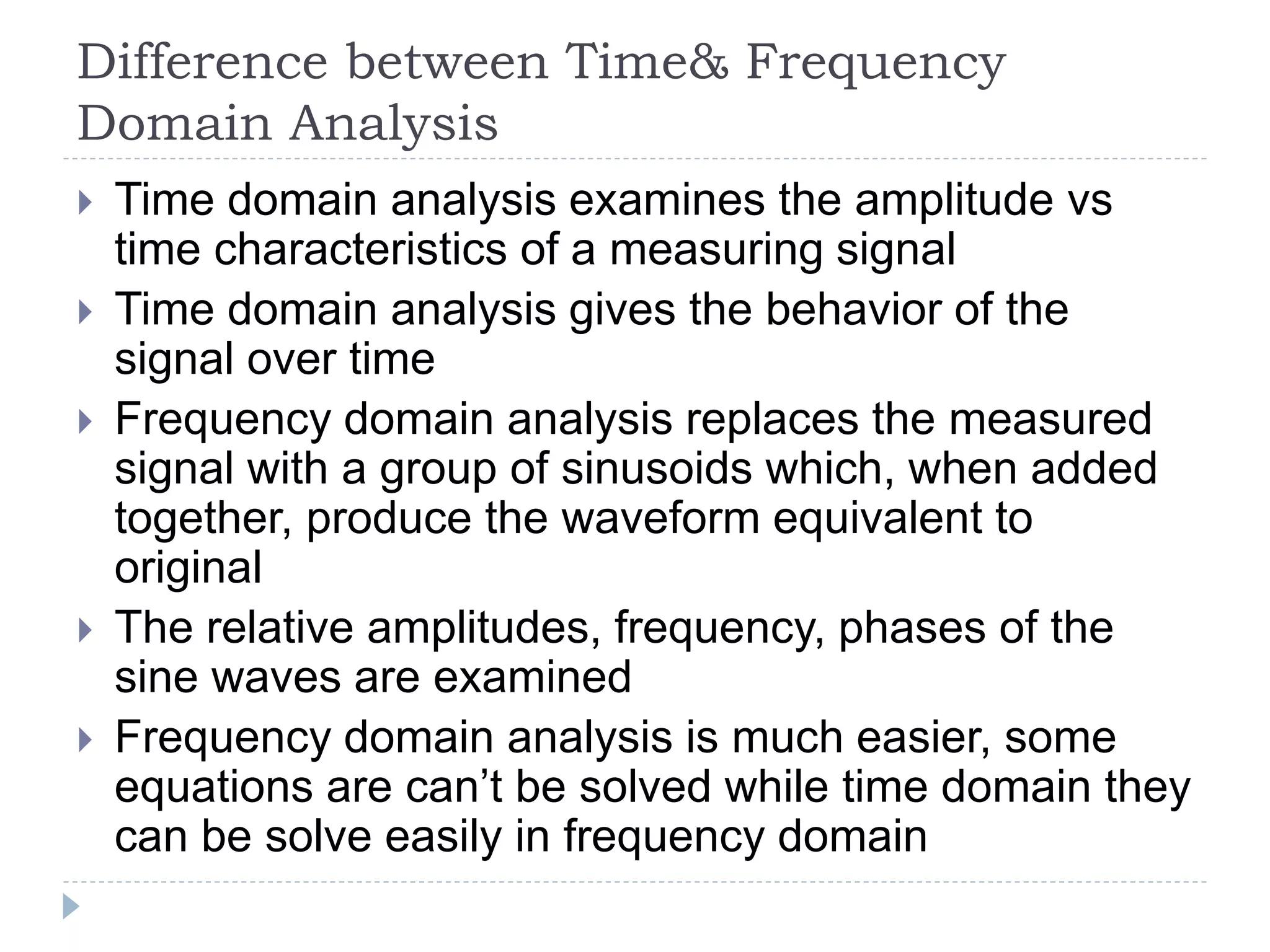
Difference between Time&Frequency
Domain Analysis
Time domain analysis examines the amplitude vs
time characteristics of a measuring signal
Time domain analysis gives the behavior of the
signal over time
Frequency domain analysis replaces the measured
signal with a group of sinusoids which, when added
together, produce the waveform equivalent to
original
The relative amplitudes, frequency, phases of the
sine waves are examined
Frequency domain analysis is much easier, some
equations are can’t be solved while time domain they
can be solve easily in frequency domain
Time Domain Analysis
Introduction
Eye pattern
Jitter
Setup/Hold Time
Rise Time/Fall Time
14.
Introduction
A graphicalrepresentation of the change of some
value with respect to time
In the time domain, the signal or function's value is
known for all real numbers, for the case
of continuous time, or at various separate instants in
the case of discrete time
A time-domain graph shows how a signal changes
with time, whereas a frequency-domain graph shows
how much of the signal lies within each given
frequency band over a range of frequencies.
15.
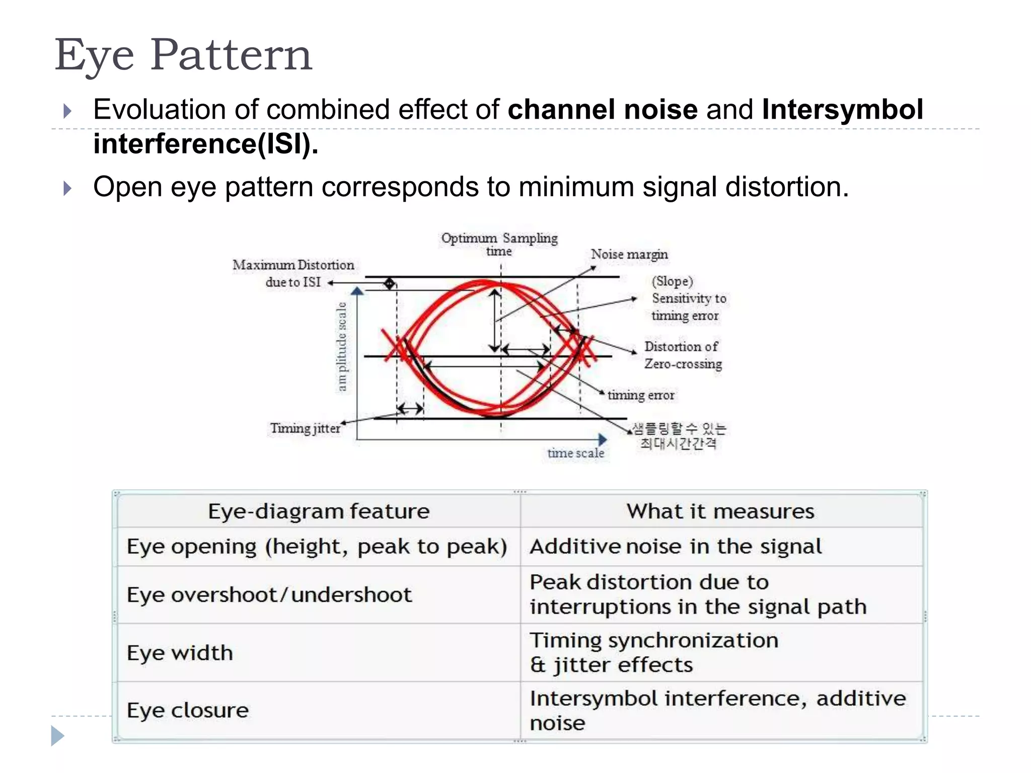
Eye Pattern
Evoluationof combined effect of channel noise and Intersymbol
interference(ISI).
Open eye pattern corresponds to minimum signal distortion.
16.
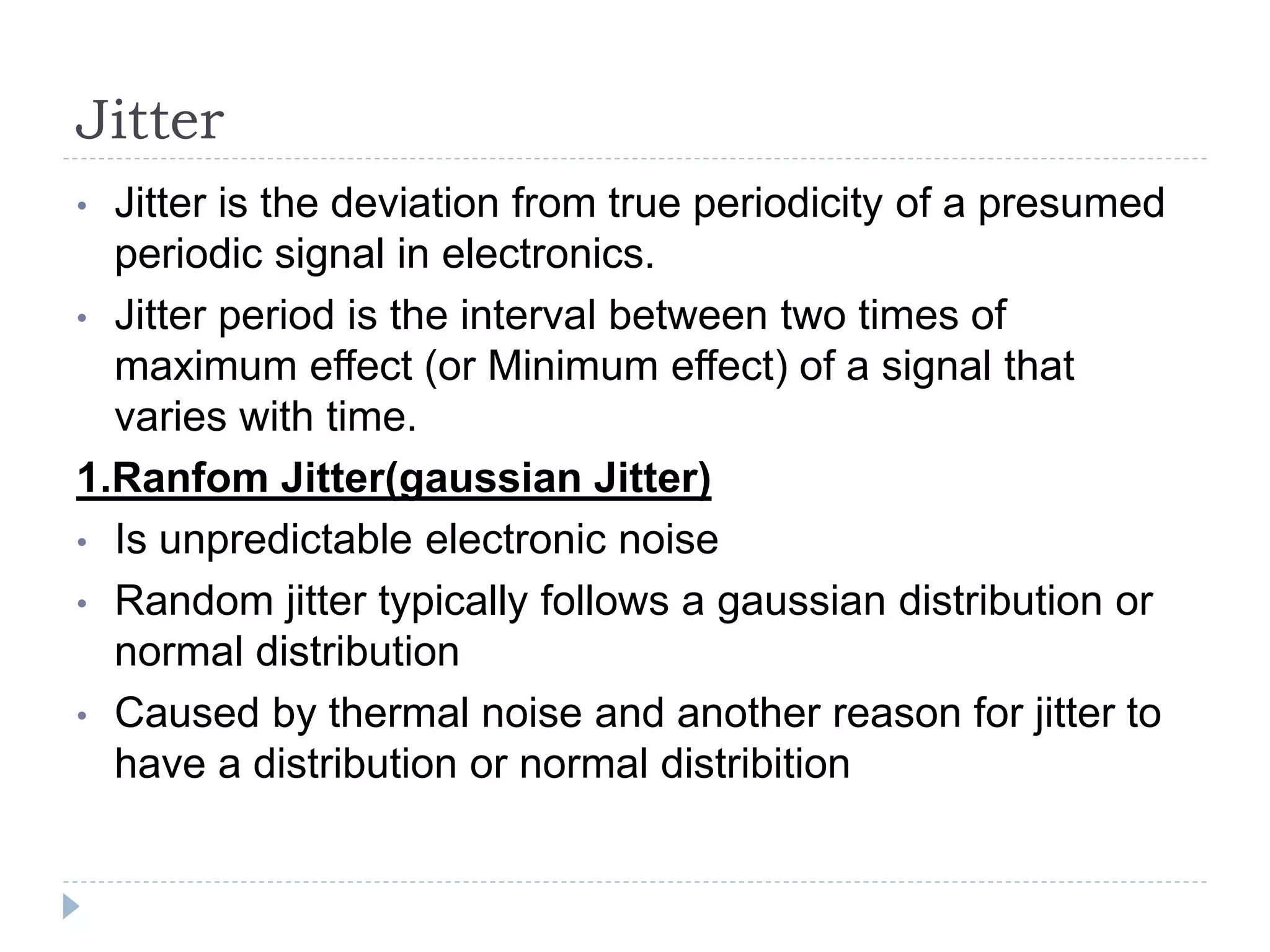
Jitter
• Jitter isthe deviation from true periodicity of a presumed
periodic signal in electronics.
• Jitter period is the interval between two times of
maximum effect (or Minimum effect) of a signal that
varies with time.
1.Ranfom Jitter(gaussian Jitter)
• Is unpredictable electronic noise
• Random jitter typically follows a gaussian distribution or
normal distribution
• Caused by thermal noise and another reason for jitter to
have a distribution or normal distribition
17.
Jitter(Cont…)
2.Deterministric Jitter
Itis a type of clock timing jitter or data signal jitter is
predictable and reproducible
The peak to peak value of this jitter is bounded and
the bounds can easily be observed and predicted
Total jitter
Total jitter (T) is the combination of random jitter (R)
and
deterministic jitter (D)
T = Dpeak-to-peak + 2× n×Rrms,
in which the value of n is based on the bit error rate
(BER) required of the link
18.
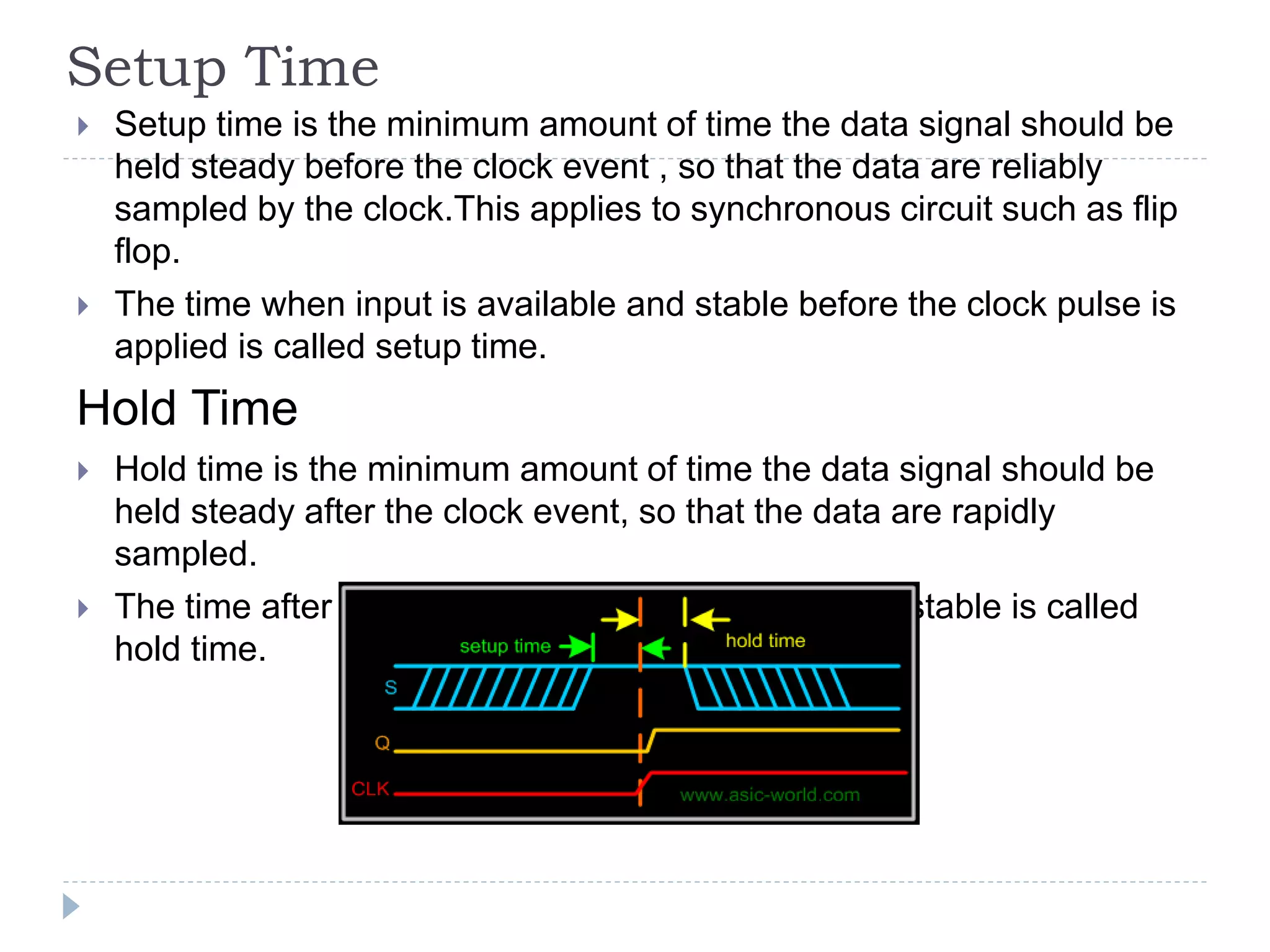
Setup Time
Setuptime is the minimum amount of time the data signal should be
held steady before the clock event , so that the data are reliably
sampled by the clock.This applies to synchronous circuit such as flip
flop.
The time when input is available and stable before the clock pulse is
applied is called setup time.
Hold Time
Hold time is the minimum amount of time the data signal should be
held steady after the clock event, so that the data are rapidly
sampled.
The time after clock pulse where data input is held stable is called
hold time.
19.
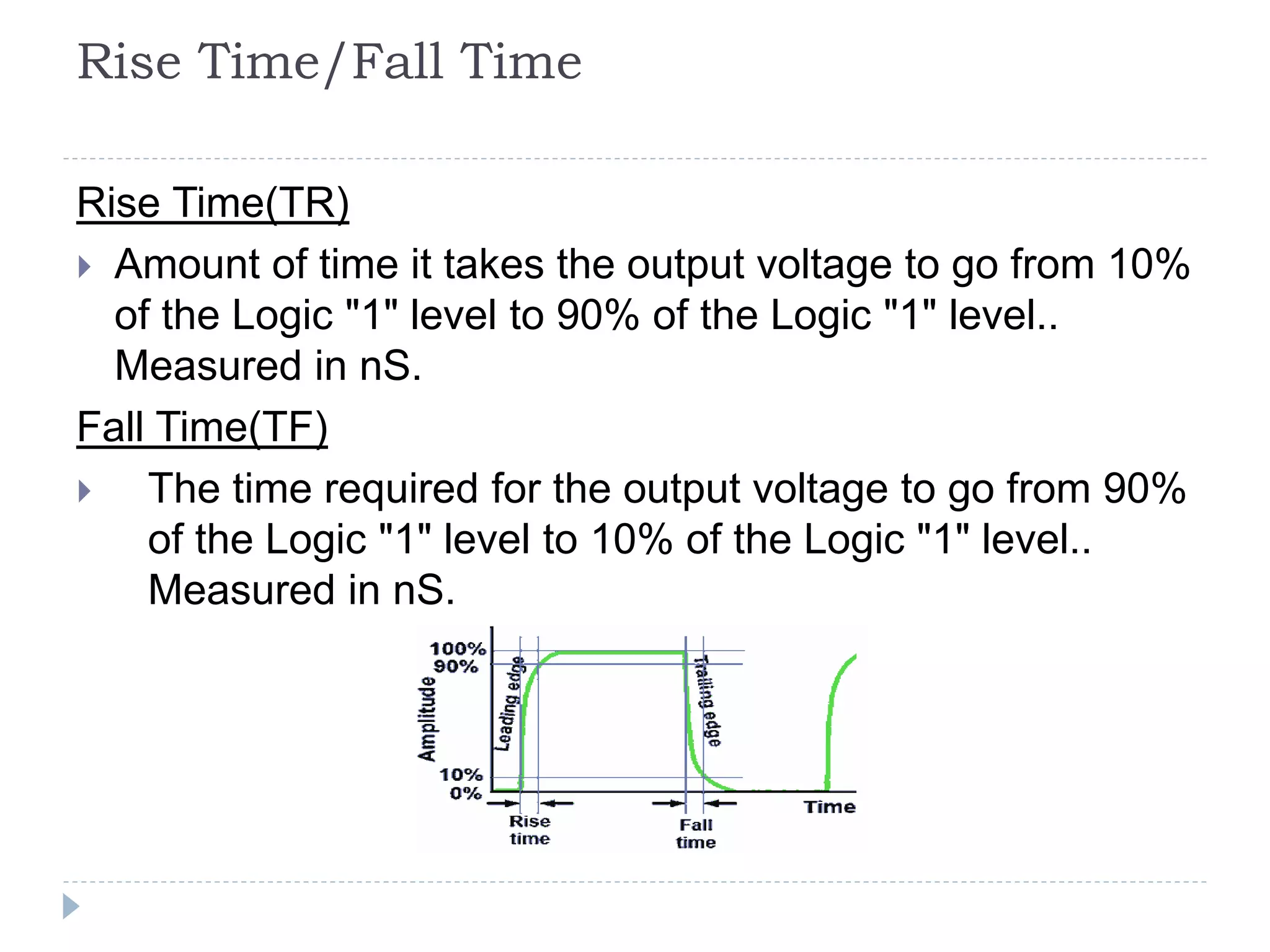
Rise Time/Fall Time
RiseTime(TR)
Amount of time it takes the output voltage to go from 10%
of the Logic "1" level to 90% of the Logic "1" level..
Measured in nS.
Fall Time(TF)
The time required for the output voltage to go from 90%
of the Logic "1" level to 10% of the Logic "1" level..
Measured in nS.
20.
Frequency Domain Analysis
Introduction
S-Parameter
Insertion Loss
Return Loss
Cross Talk
Nyquist Frequency
Knee Frequency
Skew
21.
Introduction
The frequencyresponse of a system is defined
steady state response of the system
A graphical representation of the amount of energy
present in a signal at each of many frequencies
The frequency response of a system is defined
steady state response of the system
The frequency domain values are really just a series
of sinusoidal equivalents, so amplitudes are usually
represented the same as in the time domain.
The frequency domain is usually derived by
computing a Fast Fourier Transform (FFT) of a time
domain signal.
22.
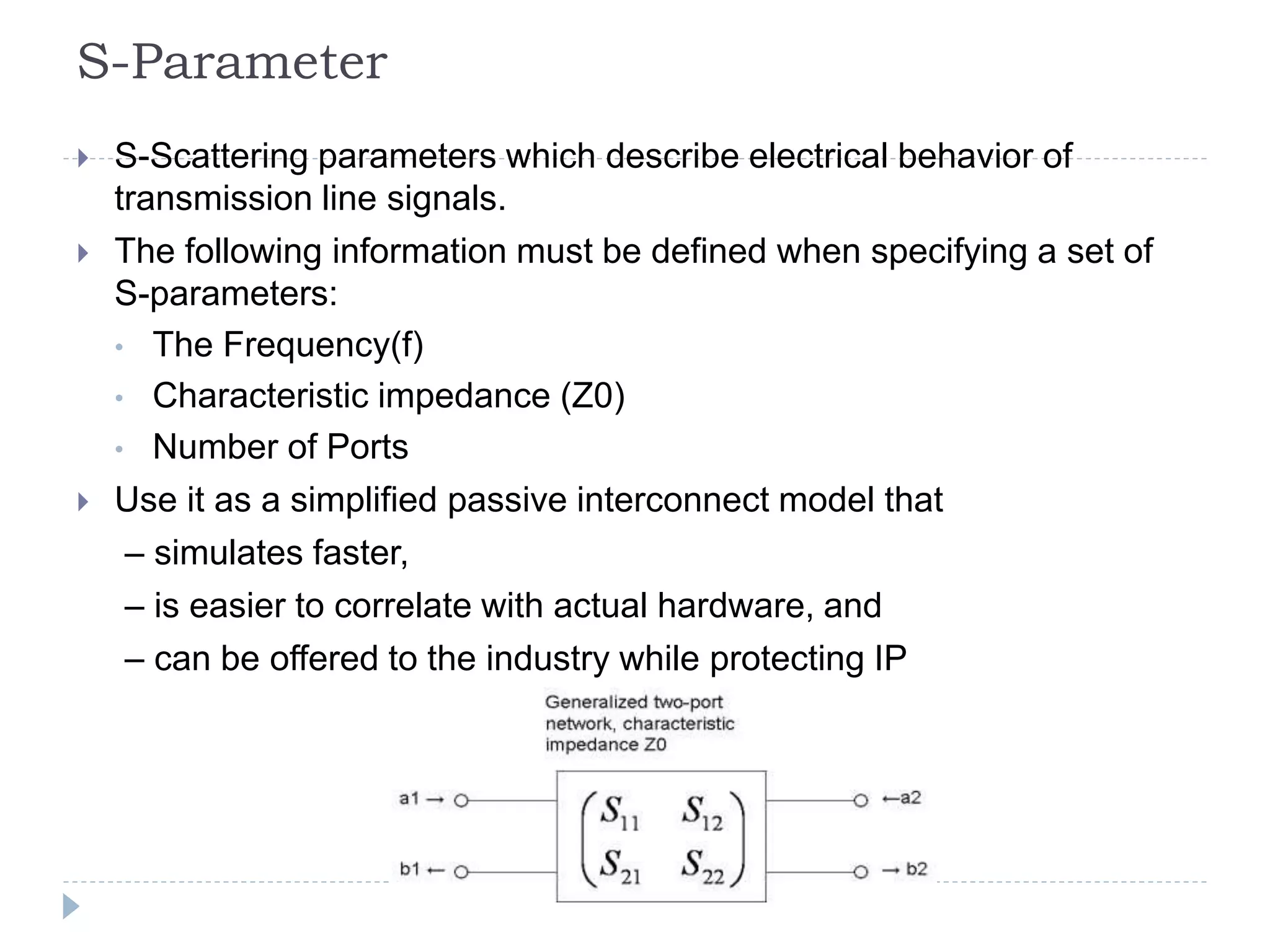
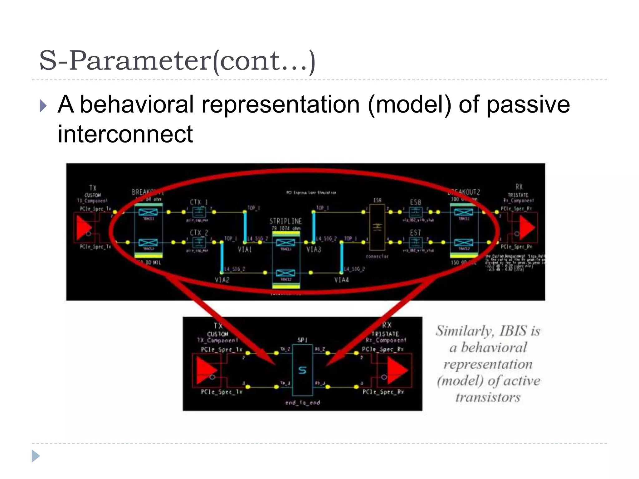
S-Parameter
S-Scattering parameterswhich describe electrical behavior of
transmission line signals.
The following information must be defined when specifying a set of
S-parameters:
• The Frequency(f)
• Characteristic impedance (Z0)
• Number of Ports
Use it as a simplified passive interconnect model that
– simulates faster,
– is easier to correlate with actual hardware, and
– can be offered to the industry while protecting IP
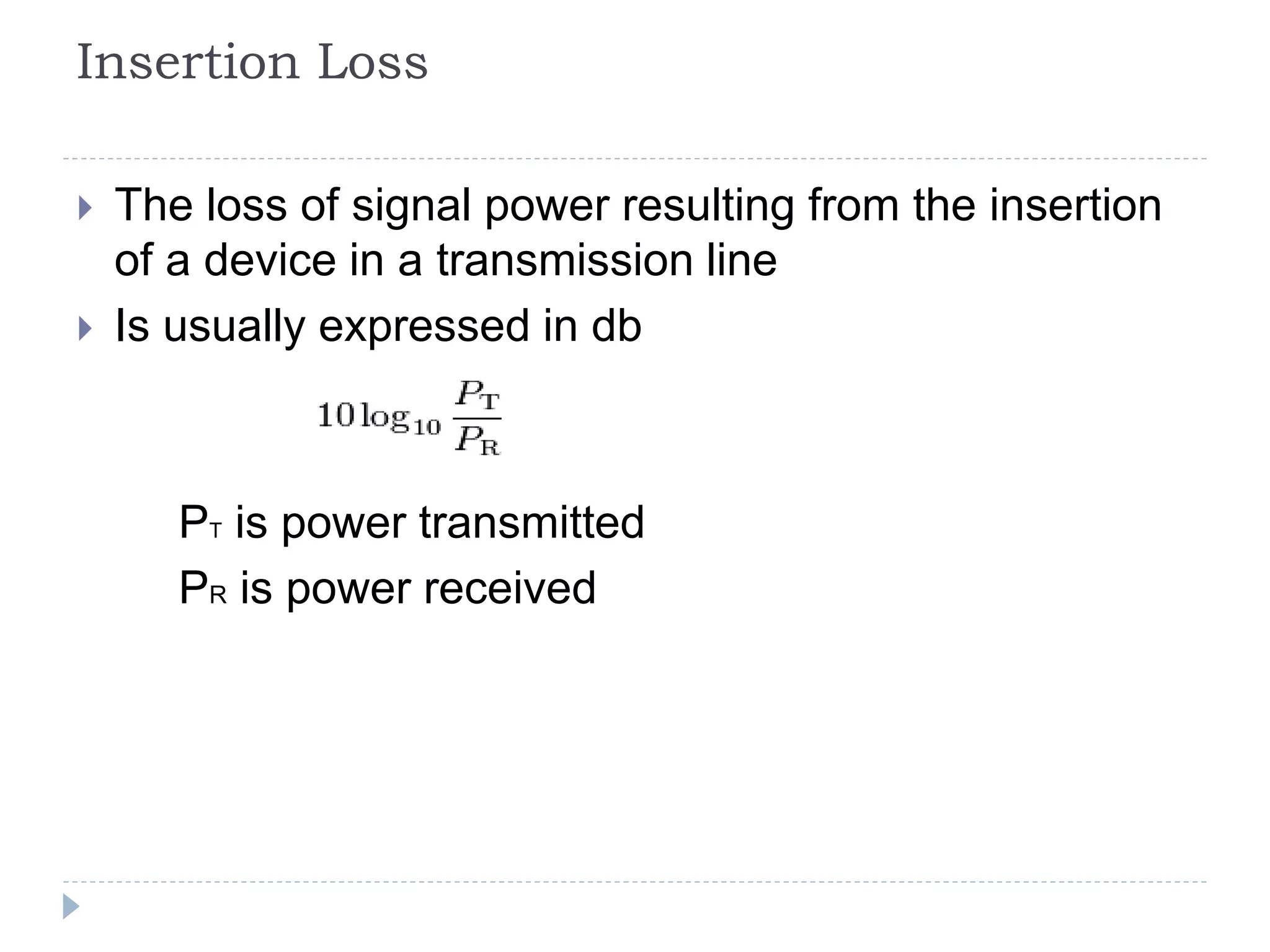
Insertion Loss
Theloss of signal power resulting from the insertion
of a device in a transmission line
Is usually expressed in db
PT is power transmitted
PR is power received
25.
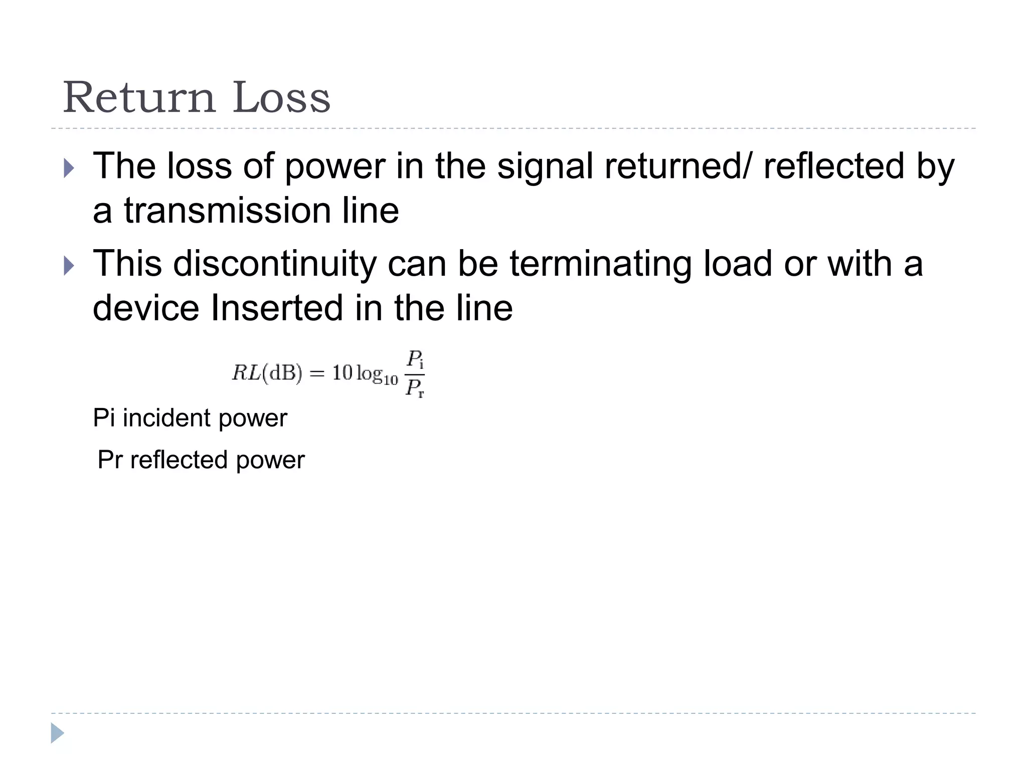
Return Loss
Theloss of power in the signal returned/ reflected by
a transmission line
This discontinuity can be terminating load or with a
device Inserted in the line
Pi incident power
Pr reflected power
26.
Cross Talk(XT)
crosstalk(XT) is any phenomenon by which
a signal transmitted on one circuit or channel of
a transmission system creates an undesired
effect in another circuit or channel.
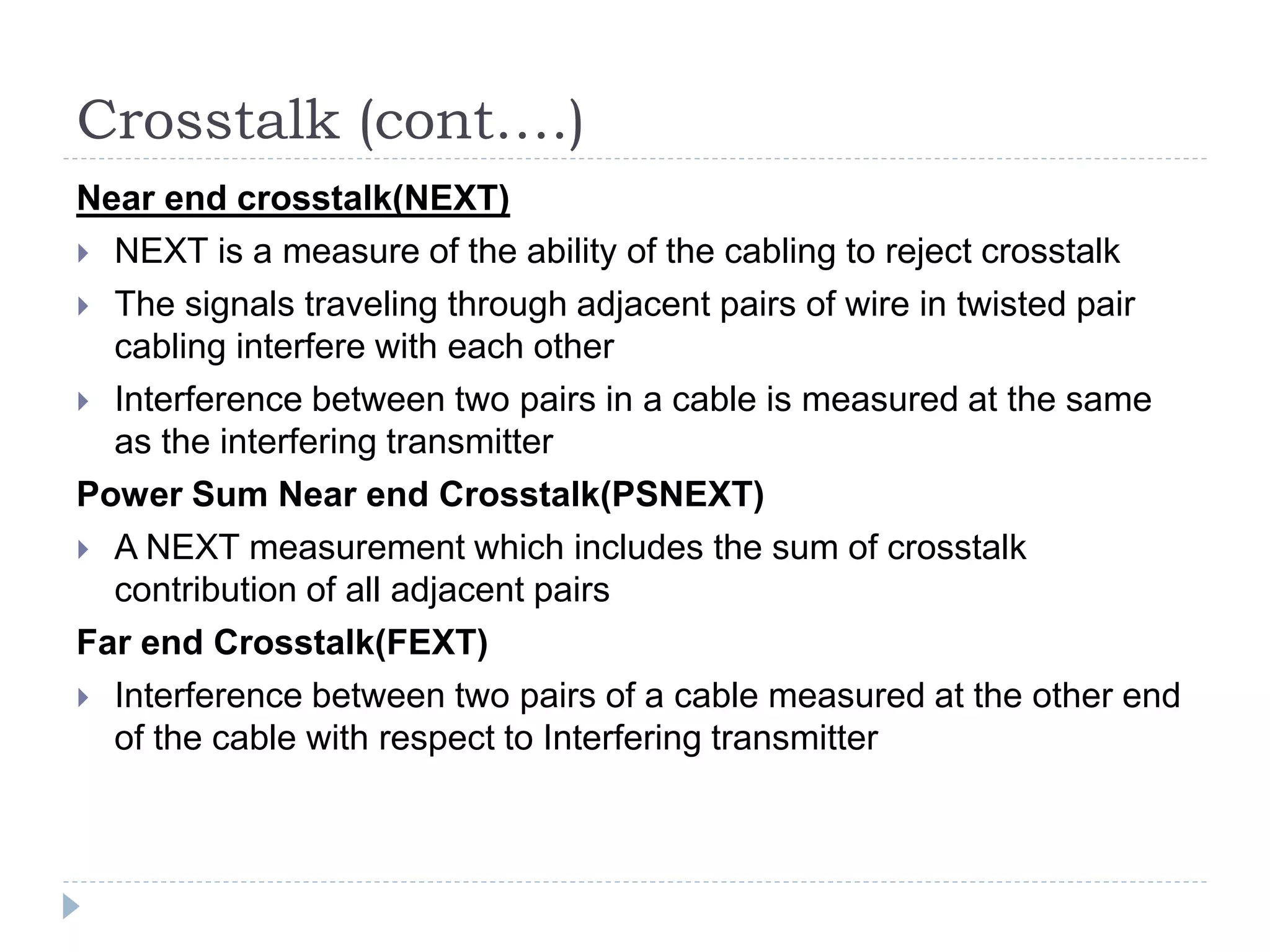
Crosstalk (cont….)
Near endcrosstalk(NEXT)
NEXT is a measure of the ability of the cabling to reject crosstalk
The signals traveling through adjacent pairs of wire in twisted pair
cabling interfere with each other
Interference between two pairs in a cable is measured at the same
as the interfering transmitter
Power Sum Near end Crosstalk(PSNEXT)
A NEXT measurement which includes the sum of crosstalk
contribution of all adjacent pairs
Far end Crosstalk(FEXT)
Interference between two pairs of a cable measured at the other end
of the cable with respect to Interfering transmitter
29.
Crosstalk (cont….)
Equal LevelFar end Crosstalk(ELEFEXT)
An FEXT measured with attenuation compensation.
Power Sum Far end Crosstalk(PSFEXT)
It is the sum of all interference signals, which are
coupled in a pair of conductors.
30.
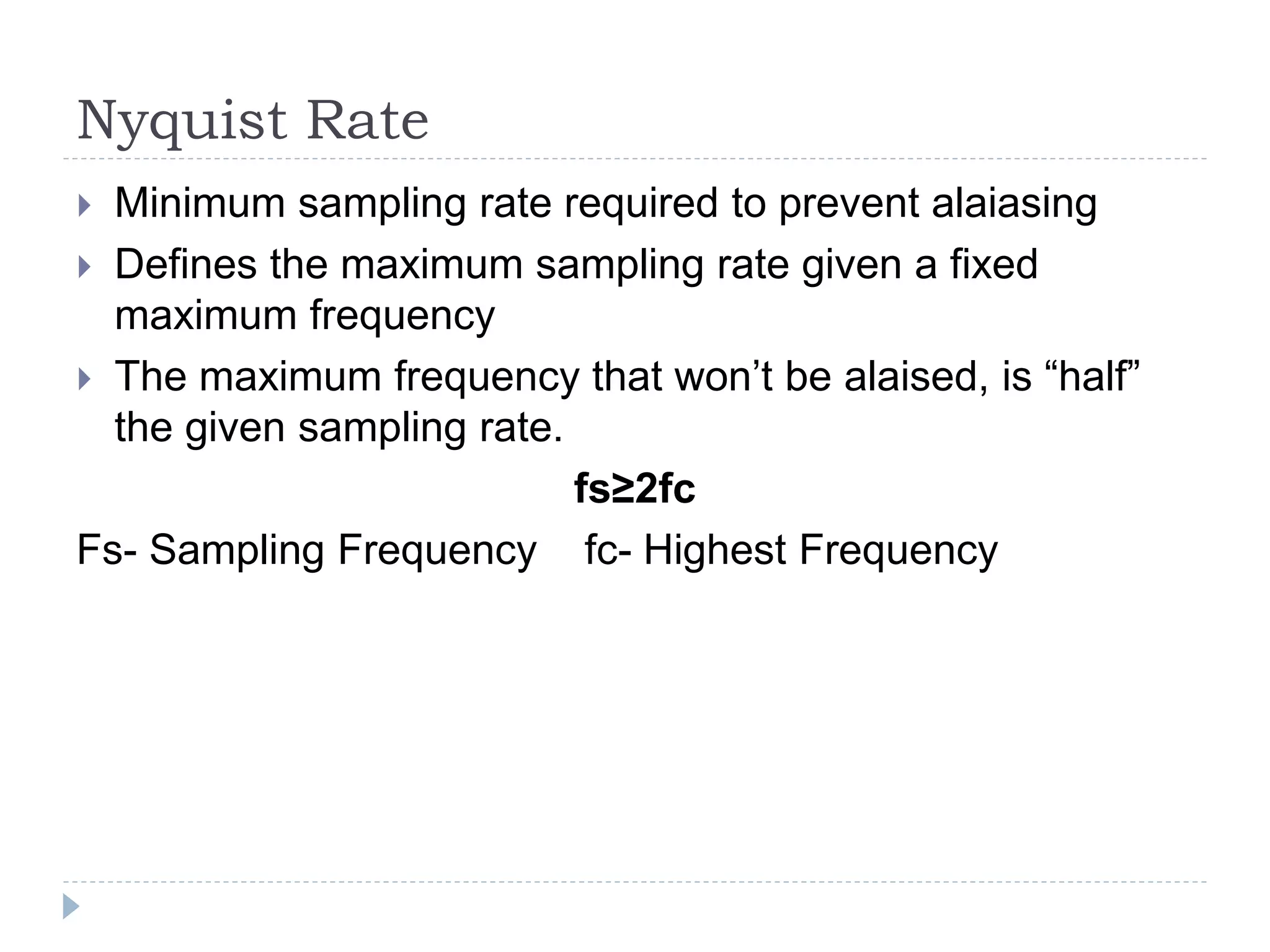
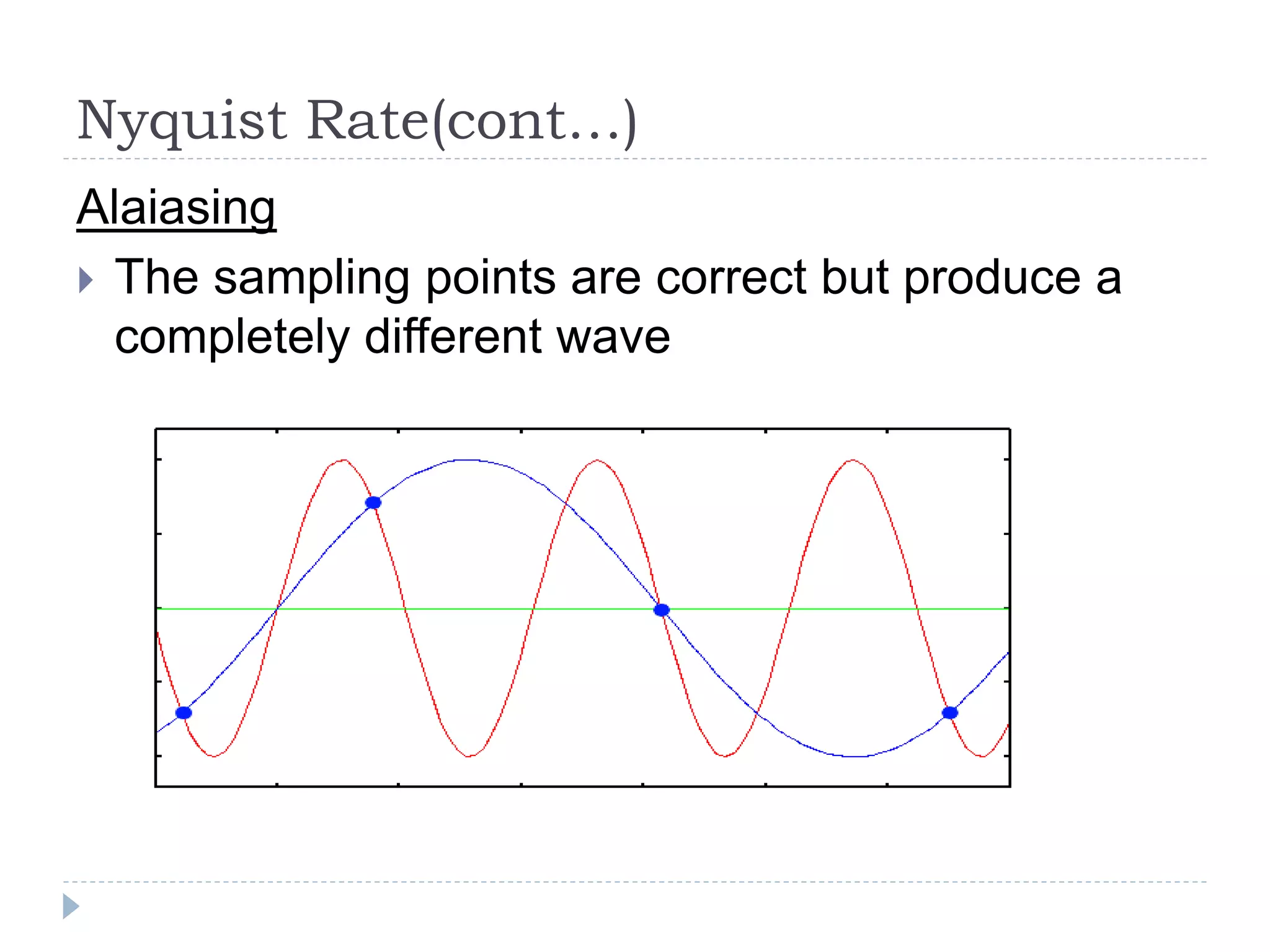
Nyquist Rate
Minimumsampling rate required to prevent alaiasing
Defines the maximum sampling rate given a fixed
maximum frequency
The maximum frequency that won’t be alaised, is “half”
the given sampling rate.
fs≥2fc
Fs- Sampling Frequency fc- Highest Frequency
Knee Frequency
Kneefrequency is an estimate of the highest frequency
content of the signal
If the Rise Time is smaller the highest frequency content
will have higher frequency
If ‘t’ denotes the 10% to 90% rise time of a signal,then an
estimate for the highest frequency content of the
signal(or)Knee Frequency given by
fmax Highest Frequency content
33.
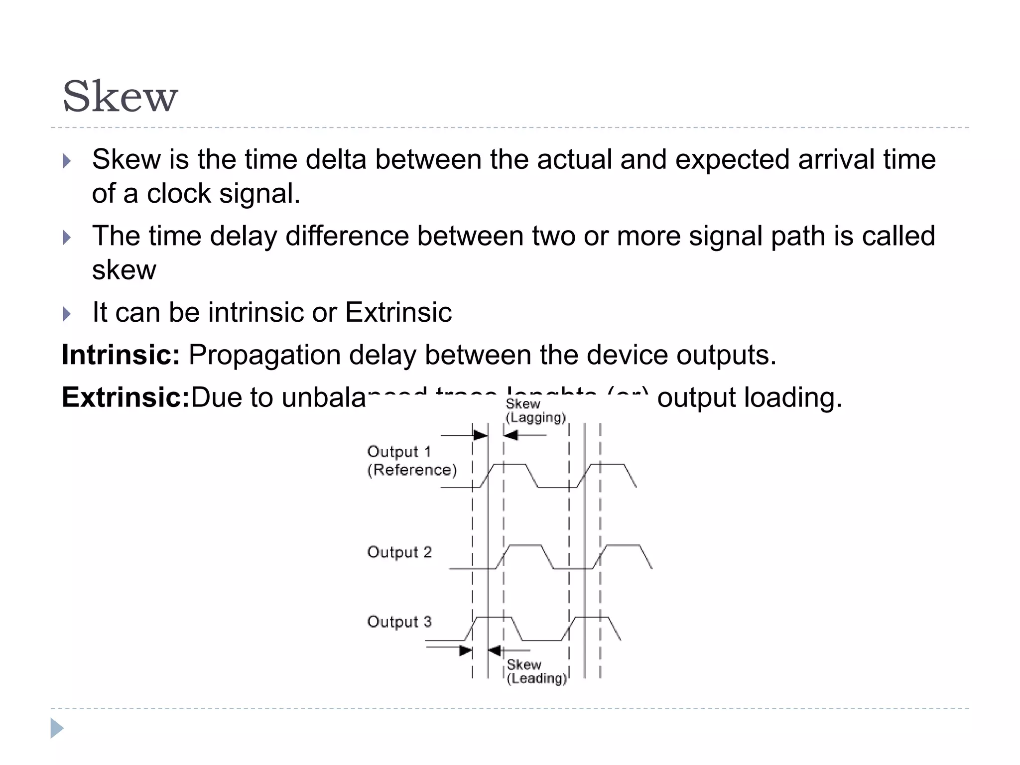
Skew
Skew isthe time delta between the actual and expected arrival time
of a clock signal.
The time delay difference between two or more signal path is called
skew
It can be intrinsic or Extrinsic
Intrinsic: Propagation delay between the device outputs.
Extrinsic:Due to unbalanced trace lenghts (or) output loading.
34.
High Speed Interfaces
DDR(Double Data Rate)
SAS(Serial Attached SCSI)
SATA(Serial Advanced Technology Attachment)
USB(Universal Serial Bus)
PCIE(Peripheral Component Interconnect Express)
35.
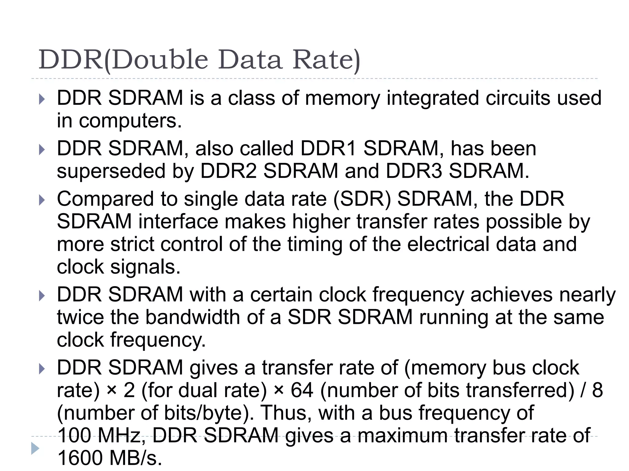
DDR(Double Data Rate)
DDR SDRAM is a class of memory integrated circuits used
in computers.
DDR SDRAM, also called DDR1 SDRAM, has been
superseded by DDR2 SDRAM and DDR3 SDRAM.
Compared to single data rate (SDR) SDRAM, the DDR
SDRAM interface makes higher transfer rates possible by
more strict control of the timing of the electrical data and
clock signals.
DDR SDRAM with a certain clock frequency achieves nearly
twice the bandwidth of a SDR SDRAM running at the same
clock frequency.
DDR SDRAM gives a transfer rate of (memory bus clock
rate) × 2 (for dual rate) × 64 (number of bits transferred) / 8
(number of bits/byte). Thus, with a bus frequency of
100 MHz, DDR SDRAM gives a maximum transfer rate of
1600 MB/s.
LRDIMM
DIMM-Dual InlineMemory Module, comprises a series of
dynamic random-access memory integrated circuits
LRDIMM-Load Reduced DIMM,this technology uses
distributed buffer approach to accomplish memory
bandwidth efficiency
Improve LRDIMM architecture for better SI or data
signals
That support higher densities than RDIMM and contain
memory buffer
LRDIMM uses in memory intensive application in data
centers ,could computing and high performance
computing(HPC) environments
38.
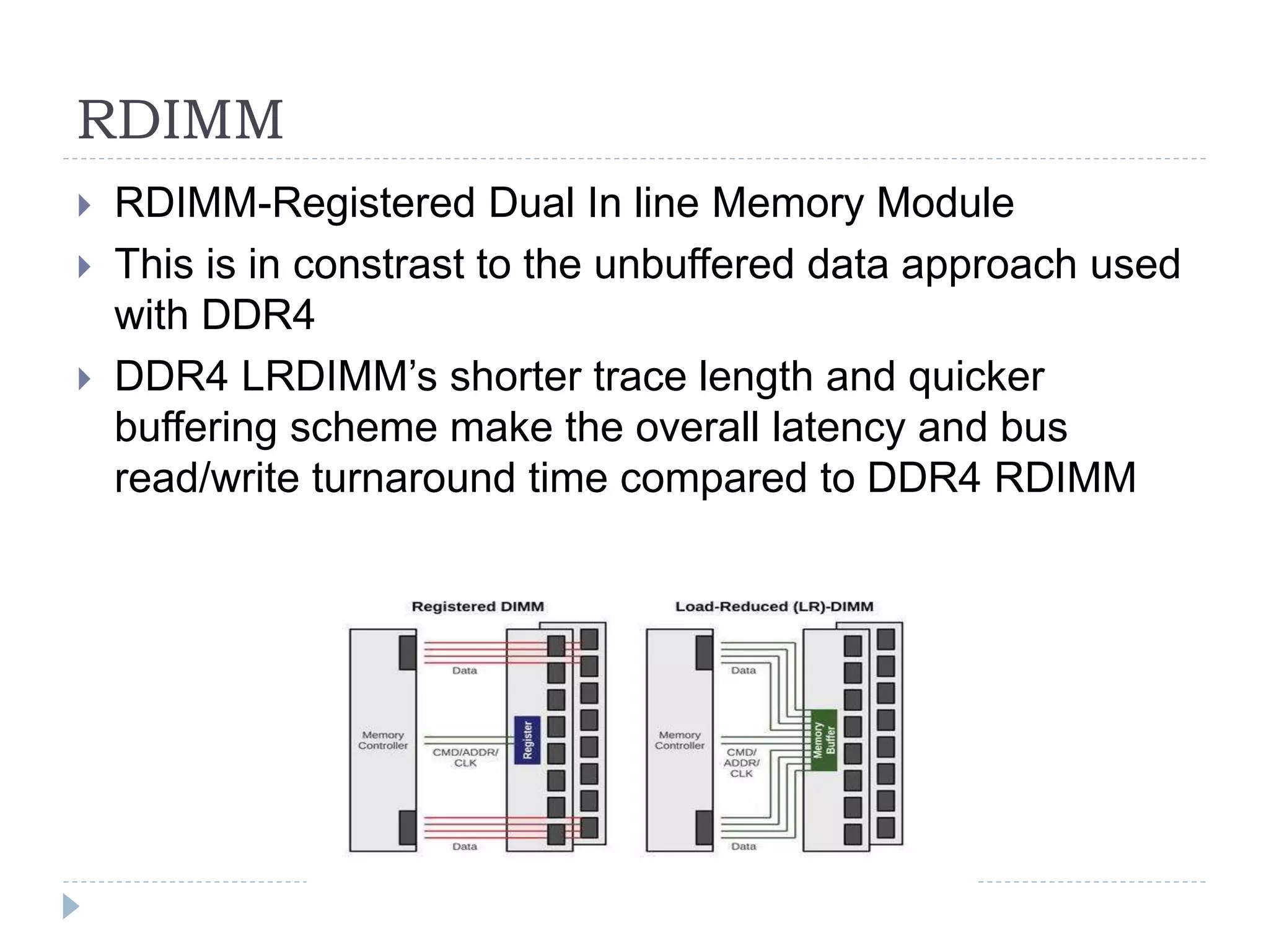
RDIMM
RDIMM-Registered DualIn line Memory Module
This is in constrast to the unbuffered data approach used
with DDR4
DDR4 LRDIMM’s shorter trace length and quicker
buffering scheme make the overall latency and bus
read/write turnaround time compared to DDR4 RDIMM
39.
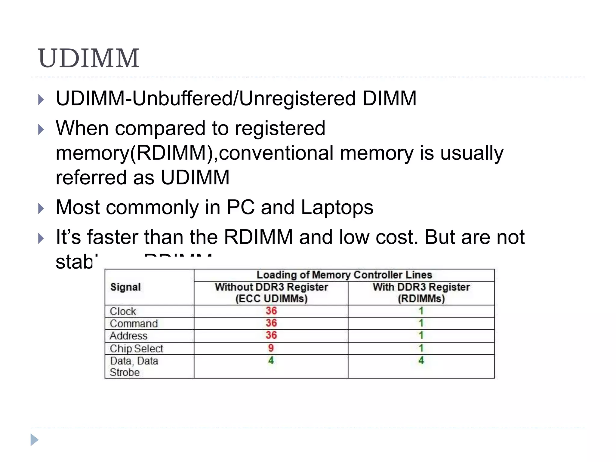
UDIMM
UDIMM-Unbuffered/Unregistered DIMM
When compared to registered
memory(RDIMM),conventional memory is usually
referred as UDIMM
Most commonly in PC and Laptops
It’s faster than the RDIMM and low cost. But are not
stable as RDIMM
40.
SAS(Serial Attached SCSI)
SCSI-Small Computer System Interface
When it was introduce the speed of SAS is 3Gbps,Then In 2009 the
speed of SAS is 6Gbps,In 2013 speed is increased to 12Gbps
It is point to point serial protocol that moves data to and from
computer storage devices
Types of component,
• Initiator-Request for processing by a target devices
• Target-Contains logical units and target ports
• Service Delivery Subsystem-I/O system transmit initiator to
target and vice versa
• Expanders-Communicate between multiple SAS devices to
initiator port
41.
SATA(Serial Advanced Technology
Attachment)
SATA is the next generation storage interface for
PCs and low-end Servers.
SATA is highly viable for servers and storage
networks
One SATA controller can aggregate multiple ports
Multiple SATA drives can be linked using backplanes
and external enclosures
SATA was designed to provide excellent speed and
storage at a low cost
Cost and scalability provides potential for greater
storage capacity at a lower cost than networked or
server storage
42.
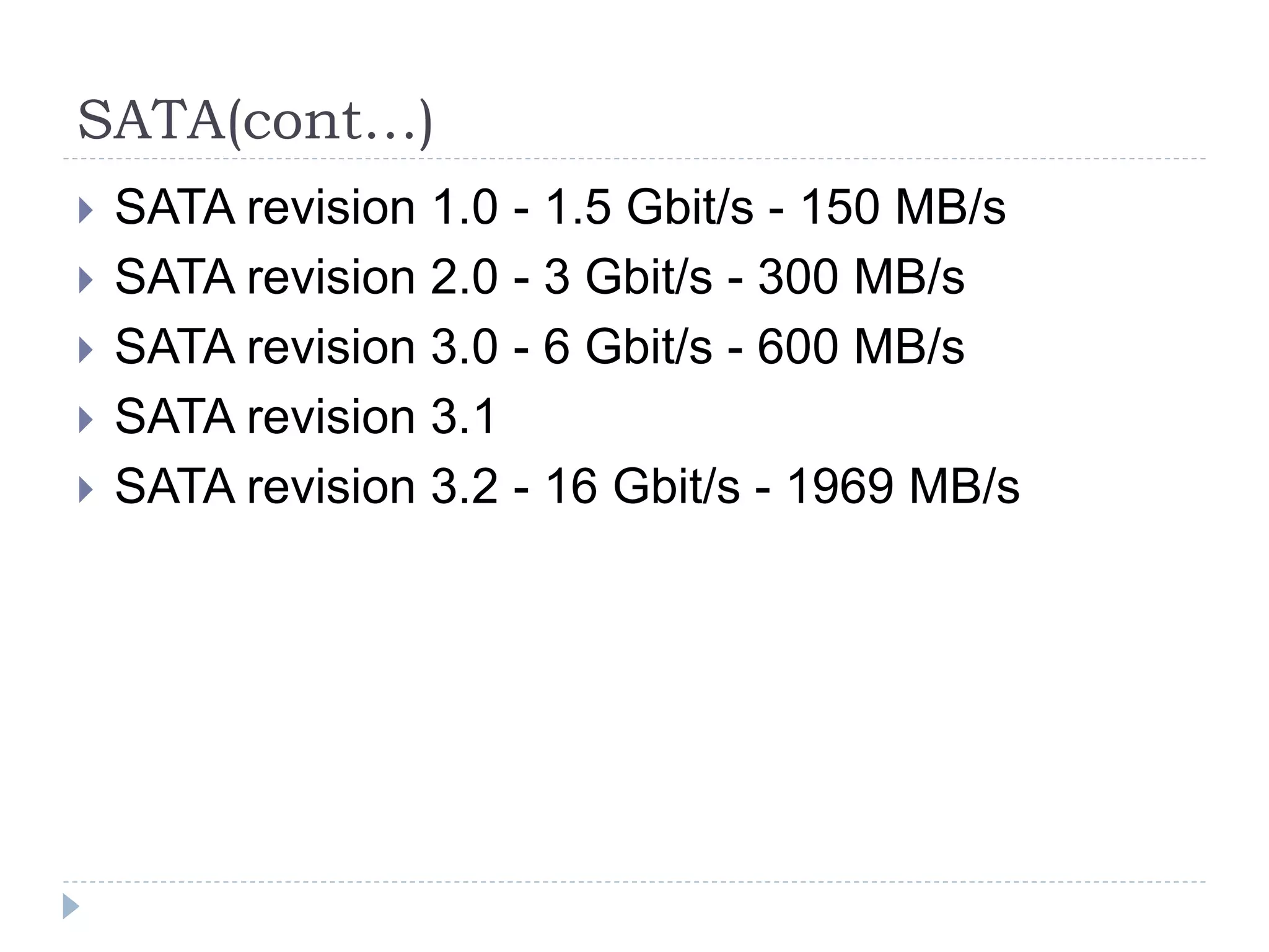
SATA(cont…)
SATA revision1.0 - 1.5 Gbit/s - 150 MB/s
SATA revision 2.0 - 3 Gbit/s - 300 MB/s
SATA revision 3.0 - 6 Gbit/s - 600 MB/s
SATA revision 3.1
SATA revision 3.2 - 16 Gbit/s - 1969 MB/s
43.
PCIe(Peripheral Component Interconnect
Express)
PCIe is a high speed serial computer expansion bus.
A computer bus is used to transfer data from one location
or device on the motherboard to the central processing
unit where all calculations take place.
PCIe has been a versatile ,function way to sonnect
sound,video and network card to a mother board.
Two different parts of a Bus
Address bus-transfers information about where the
data should go
Data bus-transfers the actual data
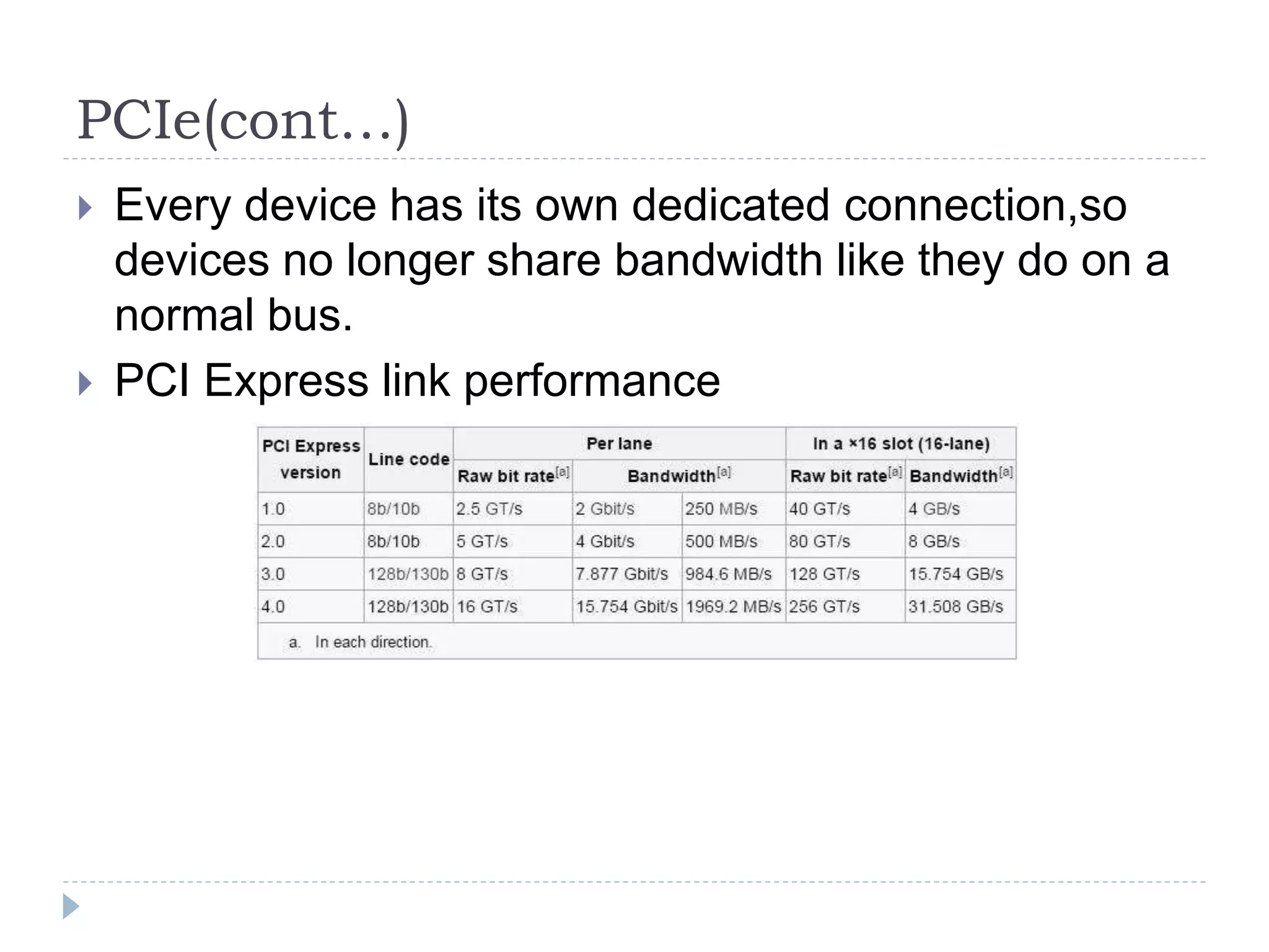
PCIe(cont…)
Every devicehas its own dedicated connection,so
devices no longer share bandwidth like they do on a
normal bus.
PCI Express link performance
46.
USB
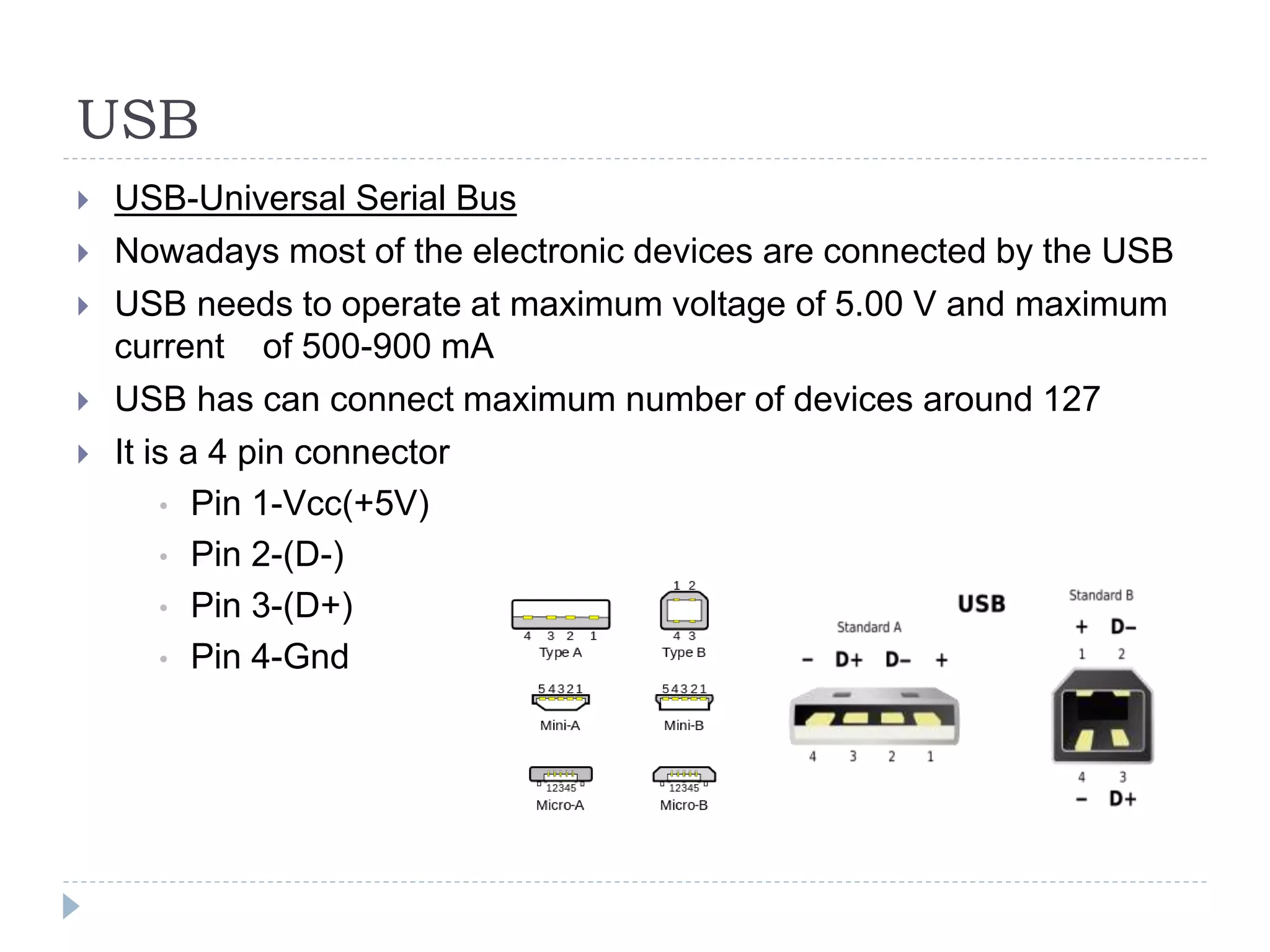
USB-Universal SerialBus
Nowadays most of the electronic devices are connected by the USB
USB needs to operate at maximum voltage of 5.00 V and maximum
current of 500-900 mA
USB has can connect maximum number of devices around 127
It is a 4 pin connector
• Pin 1-Vcc(+5V)
• Pin 2-(D-)
• Pin 3-(D+)
• Pin 4-Gnd
47.
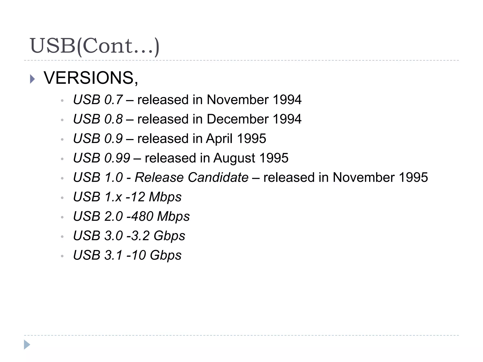
USB(Cont…)
VERSIONS,
• USB0.7 – released in November 1994
• USB 0.8 – released in December 1994
• USB 0.9 – released in April 1995
• USB 0.99 – released in August 1995
• USB 1.0 - Release Candidate – released in November 1995
• USB 1.x -12 Mbps
• USB 2.0 -480 Mbps
• USB 3.0 -3.2 Gbps
• USB 3.1 -10 Gbps
Emphasis
Emphasis isthe intentional alteration of the amplitude-vs
-frequency characteristics of the signal to reduce the
effects of noise in a communication
Pre-emphasis:
Pre-emphasis refers to boosting the relative amplitudes
of the modulating voltage for higher audio frequencies
from 2 to approximately 15 KHz.
Which boosting the relative amplitudes for high frequency
to improve the overall signal to noise ratio and the mirror
operation is called de-emphasis
pre-emphasis is done at the transmitter
50.
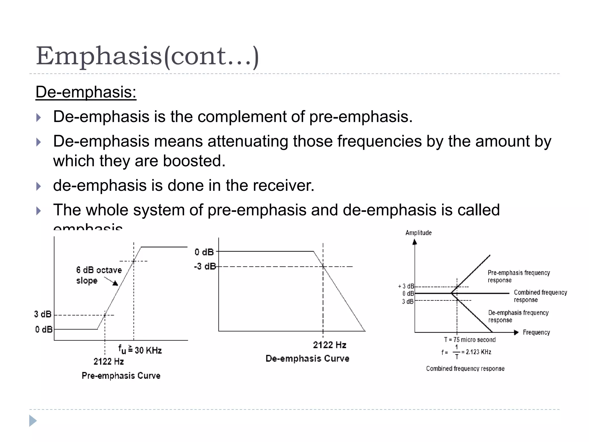
Emphasis(cont…)
De-emphasis:
De-emphasis isthe complement of pre-emphasis.
De-emphasis means attenuating those frequencies by the amount by
which they are boosted.
de-emphasis is done in the receiver.
The whole system of pre-emphasis and de-emphasis is called
emphasis
51.
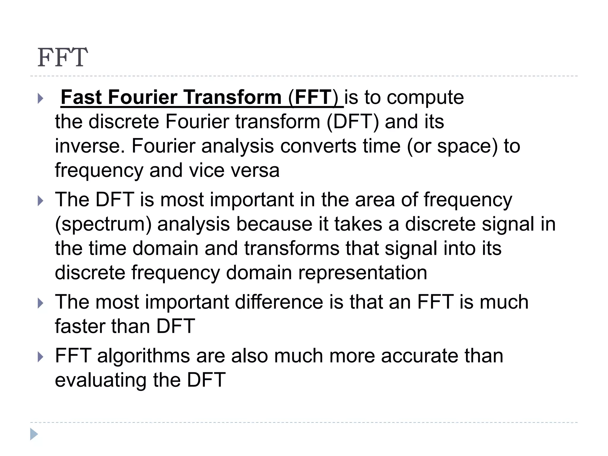
FFT
Fast FourierTransform (FFT) is to compute
the discrete Fourier transform (DFT) and its
inverse. Fourier analysis converts time (or space) to
frequency and vice versa
The DFT is most important in the area of frequency
(spectrum) analysis because it takes a discrete signal in
the time domain and transforms that signal into its
discrete frequency domain representation
The most important difference is that an FFT is much
faster than DFT
FFT algorithms are also much more accurate than
evaluating the DFT
52.
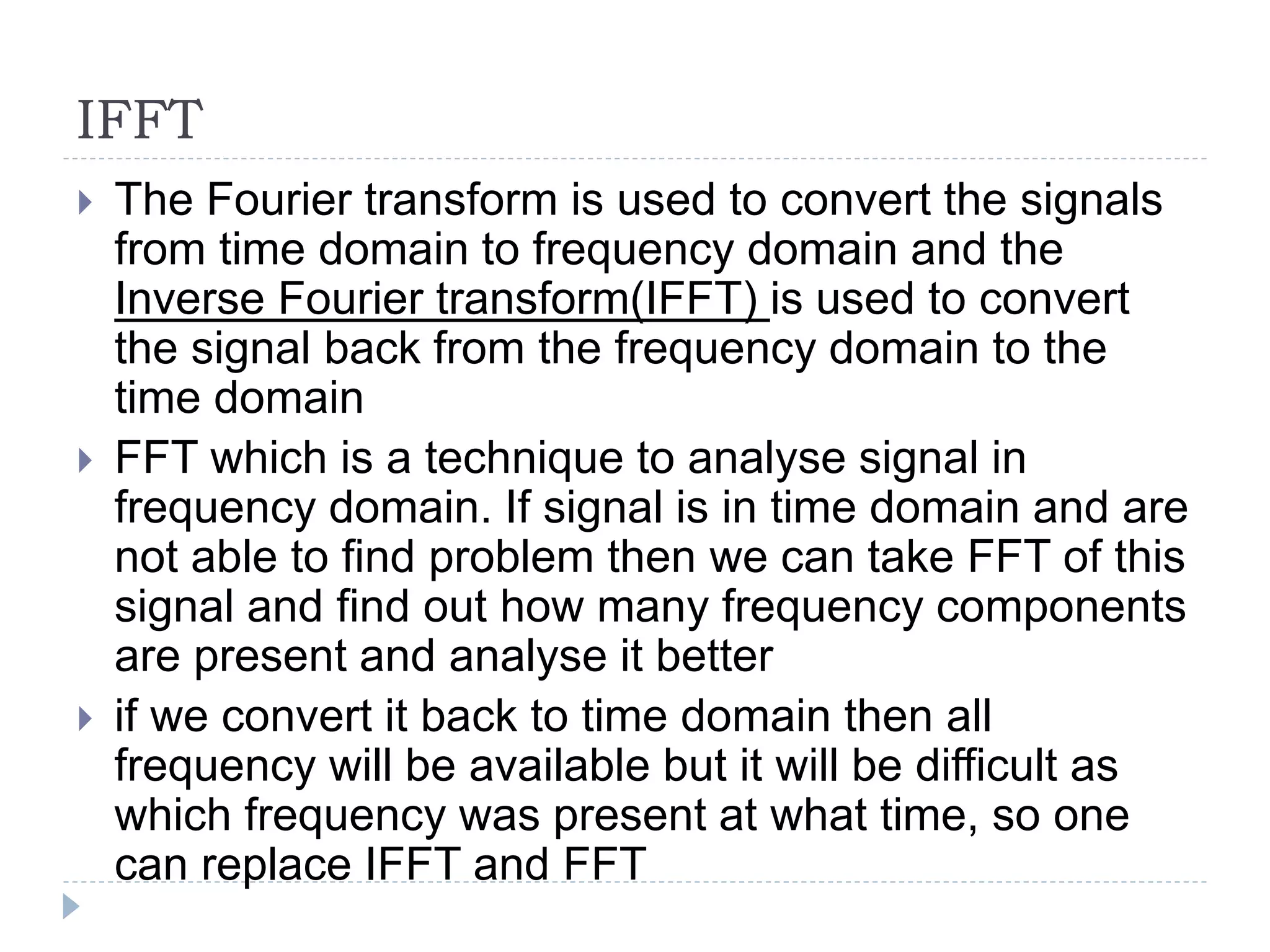
IFFT
The Fouriertransform is used to convert the signals
from time domain to frequency domain and the
Inverse Fourier transform(IFFT) is used to convert
the signal back from the frequency domain to the
time domain
FFT which is a technique to analyse signal in
frequency domain. If signal is in time domain and are
not able to find problem then we can take FFT of this
signal and find out how many frequency components
are present and analyse it better
if we convert it back to time domain then all
frequency will be available but it will be difficult as
which frequency was present at what time, so one
can replace IFFT and FFT
53.
FFE
Feed-Forward Equalization(FFE) is an equalization
technique that corrects the received waveform with
information about the waveform itself and not information
about the logical decisions made on the waveform
FFE basically acts like a FIR (finite impulse response)
filter and uses the voltage levels of the received
waveform associated with previous and current bits to
correct the voltage level of the current bit
FFE is only concerned with correcting voltage levels in
the waveform
The mathematical expression of FFE is,
e(t) = c0r(t - (0TD)) + c1r(t - (1TD)) + c2r(t - (2TD))
54.
DFE
Decision FeedbackEqualization (DFE), DFE
calculates a correction value that is added to the
logical decision threshold
The mathematical expression of FFE is,
V(k) = c1s(k - 1) + c2(k - 2)
DFE and FFE are different equalization techniques,
it is not uncommon to use both at the receiver
DFE and FFE are both useful equalization
techniques that can be used to open closed eyes at
the receiver
55.
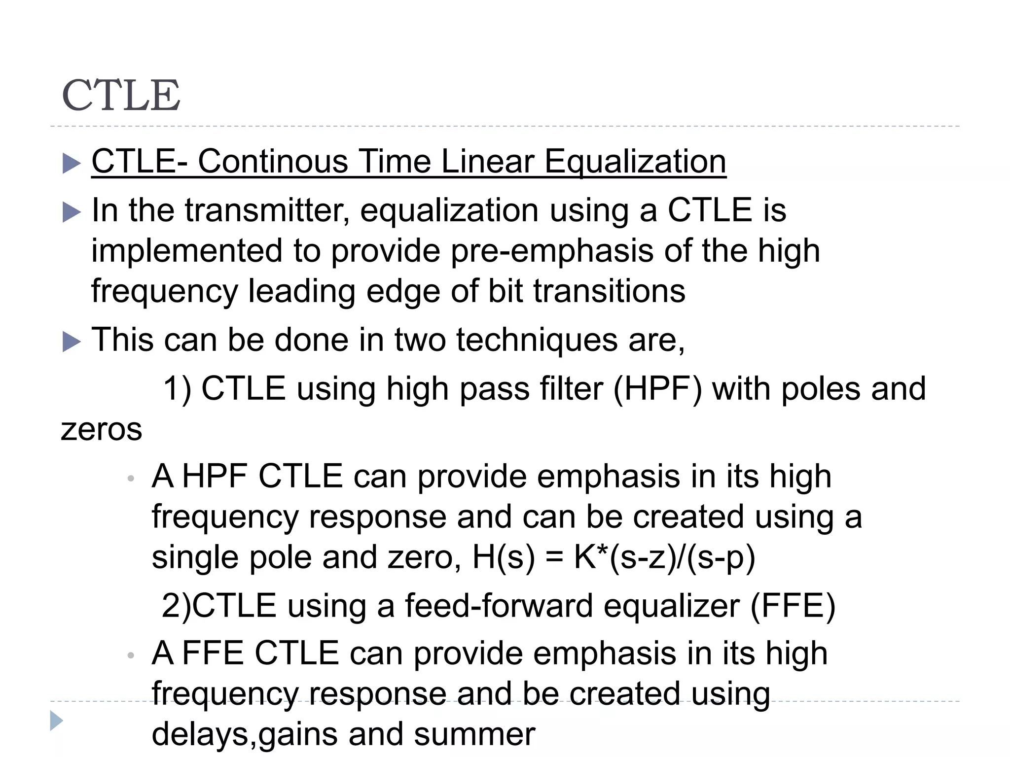
CTLE
CTLE- ContinousTime Linear Equalization
In the transmitter, equalization using a CTLE is
implemented to provide pre-emphasis of the high
frequency leading edge of bit transitions
This can be done in two techniques are,
1) CTLE using high pass filter (HPF) with poles and
zeros
• A HPF CTLE can provide emphasis in its high
frequency response and can be created using a
single pole and zero, H(s) = K*(s-z)/(s-p)
2)CTLE using a feed-forward equalizer (FFE)
• A FFE CTLE can provide emphasis in its high
frequency response and be created using
delays,gains and summer
56.
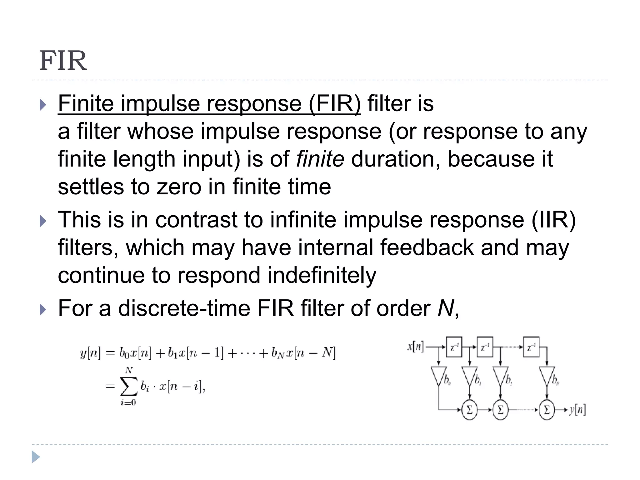
FIR
Finite impulseresponse (FIR) filter is
a filter whose impulse response (or response to any
finite length input) is of finite duration, because it
settles to zero in finite time
This is in contrast to infinite impulse response (IIR)
filters, which may have internal feedback and may
continue to respond indefinitely
For a discrete-time FIR filter of order N,
57.
3D Modeling
Introduction
MOM-Method Of Moments(2D)
Quasi Static Modeling(2.5D)
FEM-Finite Element Modeling(3D)
FDTD-Finite Difference Time Domain(3D)
58.
Introduction
Advantages ofSimulation Modeling are,
• Optimize the geometry for strength and weight
• Select materials that meet weight, strength, and budget
requirements
• Simulate part failure and identify the loading conditions
that cause them
59.
MOM
MOM-Method OfMoments
Analyzing PCB with respect to radiated emission and
radiated susceptibility in the frequency domain
Can be used for analyzing any planar structure
EMC applications-Electro magnetic
compatability,shall not generate EM disturbance
60.
Quasi Static Modeling(2.5D)
FDTD-Finite Difference Time Domain Method
Numerical Analysis technique
FDTD can cover wide range frequency with a signal
simulation
It will used in a non linear material property
FDTD uses the E and H fields directly. Since most
EMI/EMC modelling applications are interested in
the E and H fields
61.
FEM
FEM-Finite ElementModelling
It is a numerical technique for finding approximate
solutions to boundary value problems for partial
differential equations
It uses subdivision of a whole problem domain into
simpler parts, called finite elements
from the calculations of variations to solve the
problem by minimizing an associated error function
It will solve electro magnetic field(TE,TM,TEM)
62.
FDTD
FDTD-Finite DifferenceTime Domain Method
Numerical Analysis technique
FDTD can cover wide range frequency with a signal
simulation
It will used in a non linear material property
FDTD uses the E and H fields directly. Since most
EMI/EMC modelling applications are interested in
the E and H fields
63.
DESIGN OF EXPERIMENTS
It is a design of any information gathering exercise
where variation is present
These statics used for controlled experiments
Advantages of DOE,
• Reliability is increased
• Shorter development time
• Process performing normal
• Cost is less
• Reduction of process variation
64.
GENETIC ALGORITHM
Geneticalgorithm(GA) is a heuristic that mimics the
process of natural selection
Heuristic is designed for solving problem more
quickly
GA which generates solution to optimization problem
using techniques inspired by natural evolution
65.
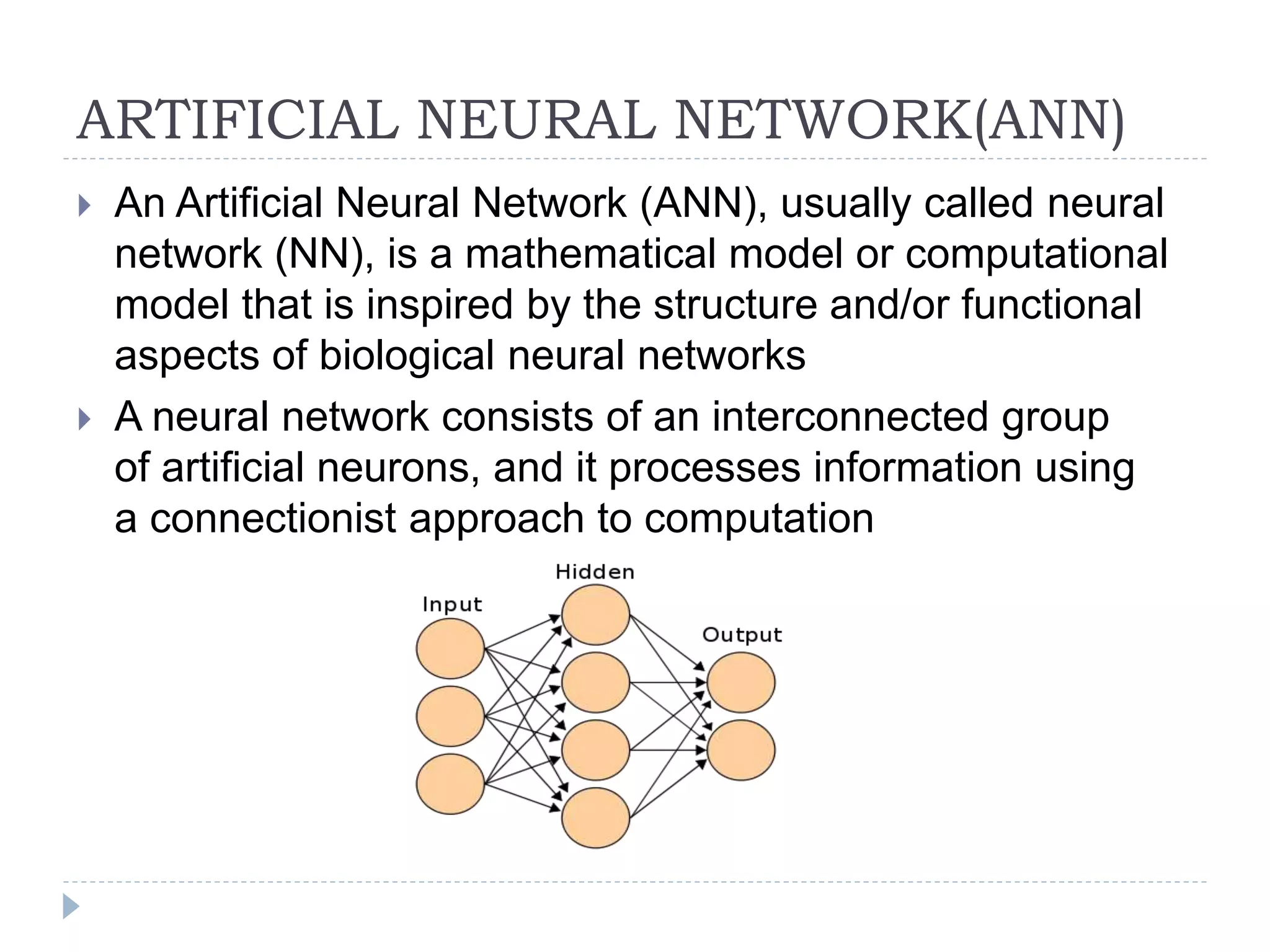
ARTIFICIAL NEURAL NETWORK(ANN)
An Artificial Neural Network (ANN), usually called neural
network (NN), is a mathematical model or computational
model that is inspired by the structure and/or functional
aspects of biological neural networks
A neural network consists of an interconnected group
of artificial neurons, and it processes information using
a connectionist approach to computation
66.
HFSS-High Frequency StructuralSimulator
Solution Types:
Driven Modal: Use this type of solution for passive high frequency
structures such as microstrips, waveguides, and transmission lines.
Driven Terminal: Use this type for simulations that deal with
signal integrity for models that have multi-conductor transmission lines.
Eigenmode: Use this type to calculate resonances of a given
structure(e.g. filters).
Transient: Use this type to employ time-domain solutions for
simulations with pulsed excitations such as ultra-wide band antennas.


![Signal Integrity - A Crash Course [R Lott]](https://cdn.slidesharecdn.com/ss_thumbnails/1cb0870c-cad3-4a68-ad41-8e9450fec5d8-170217191645-thumbnail.jpg?width=640&height=640&fit=bounds)


