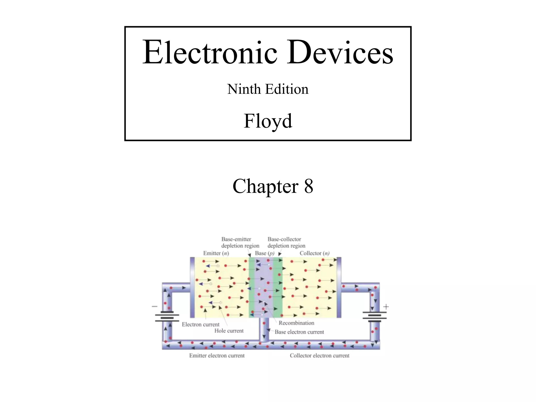
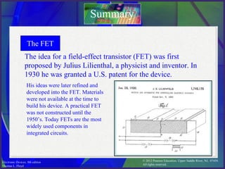
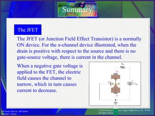
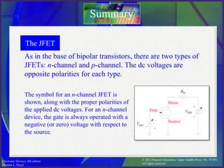
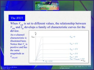
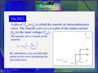
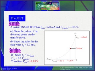
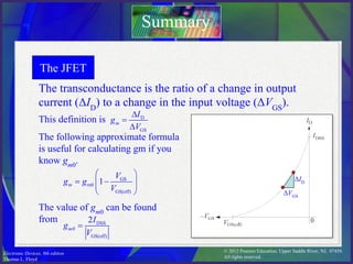
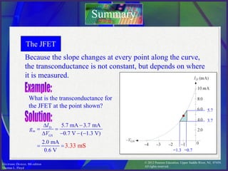
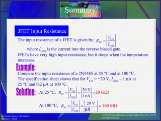
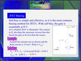
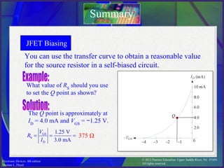
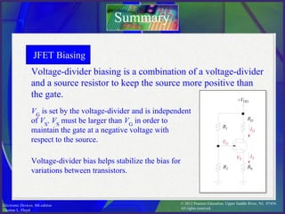
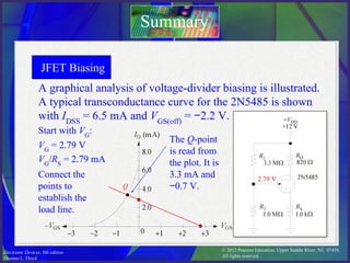
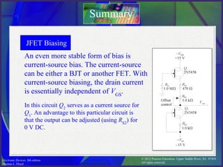
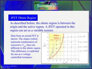
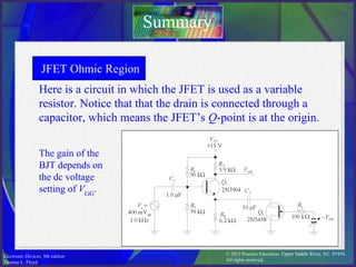
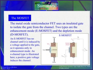
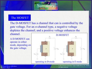
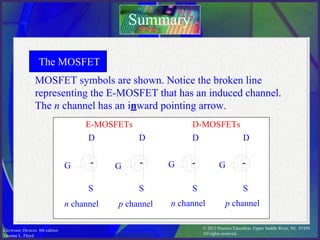
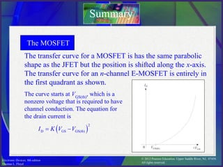
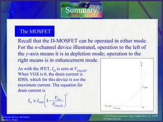
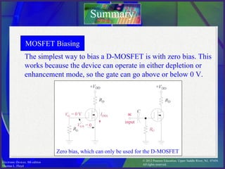
SlideShare a Scribd company logo
© 2012 Pearson Education. Upper Saddle River, NJ, 07458.
All rights reserved.
Electronic Devices, 9th edition
Thomas L. Floyd
Electronic Devices
Ninth Edition
Floyd
Chapter 8
© 2012 Pearson Education. Upper Saddle River, NJ, 07458.
All rights reserved.
Electronic Devices, 9th edition
Thomas L. Floyd
The FET
The idea for a field-effect transistor (FET) was first
proposed by Julius Lilienthal, a physicist and inventor. In
1930 he was granted a U.S. patent for the device.
Summary
His ideas were later refined and
developed into the FET. Materials
were not available at the time to
build his device. A practical FET
was not constructed until the
1950’s. Today FETs are the most
widely used components in
integrated circuits.
© 2012 Pearson Education. Upper Saddle River, NJ, 07458.
All rights reserved.
Electronic Devices, 9th edition
Thomas L. Floyd
The JFET
The JFET (or Junction Field Effect Transistor) is a normally
ON device. For the n-channel device illustrated, when the
drain is positive with respect to the source and there is no
gate-source voltage, there is current in the channel.
Summary
When a negative gate voltage is
applied to the FET, the electric
field causes the channel to
narrow, which in turn causes
current to decrease.
© 2012 Pearson Education. Upper Saddle River, NJ, 07458.
All rights reserved.
Electronic Devices, 9th edition
Thomas L. Floyd
The JFET
As in the base of bipolar transistors, there are two types of
JFETs: n-channel and p-channel. The dc voltages are
opposite polarities for each type.
Summary
The symbol for an n-channel JFET is
shown, along with the proper polarities of
the applied dc voltages. For an n-channel
device, the gate is always operated with a
negative (or zero) voltage with respect to
the source.
Gate
Source
Drain
© 2012 Pearson Education. Upper Saddle River, NJ, 07458.
All rights reserved.
Electronic Devices, 9th edition
Thomas L. Floyd
The JFET
There are three regions in the characteristic curve for a JFET
as illustrated for the case when VGS
= 0 V.
Summary
Between A and B is the Ohmic
region, where current and voltage
are related by Ohm’s law.
From B to C is the active (or
constant-current) region where
current is essentially independent
of VDS
.
Beyond C is the breakdown
region. Operation here can
damage the FET.
Ohmic region
Active region
(constant current)
(pinch-off voltage)
Breakdown
VGS
= 0
© 2012 Pearson Education. Upper Saddle River, NJ, 07458.
All rights reserved.
Electronic Devices, 9th edition
Thomas L. Floyd
The JFET
When VGS
is set to different values, the relationship between
VDS
and ID
develops a family of characteristic curves for the
device.
Summary
An n-channel
characteristic is
illustrated here.
Notice that Vp
is
positive and has
the same
magnitude as
VGS(off)
.
© 2012 Pearson Education. Upper Saddle River, NJ, 07458.
All rights reserved.
Electronic Devices, 9th edition
Thomas L. Floyd
The JFET
A plot of VGS
to ID
is called the transfer or transconductance
curve. The transfer curve is a is a plot of the output current
(ID
) to the input voltage (VGS
).
Summary
The transfer curve is based on the
equation
By substitution, you can find other
points on the curve for plotting the
universal curve.
IDSS
2
0.3 VGS(off)
0.5 VGS(off)
IDSS
4
© 2012 Pearson Education. Upper Saddle River, NJ, 07458.
All rights reserved.
Electronic Devices, 9th edition
Thomas L. Floyd
The JFET
A certain 2N5458 JFET has IDSS
= 6.0 mA and VGS(off)
= – 3.5 V.
Summary
(a) Show the values of the
these end points on the
transfer curve.
(b) Show the point for the
case when ID
= 3.0 mA.
= 6.0 mA
= −3.5 V
(b) When ID
= ½ IDSS
,
VGS
= 0.3 VGS(off)
.
Therefore, VGS
= −1.05 V −1.05 V
3.0 mA
© 2012 Pearson Education. Upper Saddle River, NJ, 07458.
All rights reserved.
Electronic Devices, 9th edition
Thomas L. Floyd
The JFET
The transconductance is the ratio of a change in output
current (ΔID
) to a change in the input voltage (ΔVGS
).
Summary
The following approximate formula
is useful for calculating gm if you
know gm0
.
ΔID
ΔVGS
The value of gm0
can be found
from
This definition is
© 2012 Pearson Education. Upper Saddle River, NJ, 07458.
All rights reserved.
Electronic Devices, 9th edition
Thomas L. Floyd
The JFET
Because the slope changes at every point along the curve,
the transconductance is not constant, but depends on where
it is measured.
Summary
What is the transconductance for
the JFET at the point shown?
5.7
3.7
−0.7
−1.3
3.33 mS
© 2012 Pearson Education. Upper Saddle River, NJ, 07458.
All rights reserved.
Electronic Devices, 9th edition
Thomas L. Floyd
The input resistance of a JFET is given by:
Summary
JFET Input Resistance
Compare the input resistance of a 2N5485 at 25 o
C and at 100 o
C.
The specification sheet shows that for VGS
= −20 V, IGSS
– 1 nA at
25 o
C and 0.2 μA at 100 o
C.
At 25 o
C,
where IGSS
is the current into the reverse biased gate.
20 GΩ!
JFETs have very high input resistance, but it drops when the temperature
increases.
At 100 o
C, 100 MΩ
© 2012 Pearson Education. Upper Saddle River, NJ, 07458.
All rights reserved.
Electronic Devices, 9th edition
Thomas L. Floyd
JFET Biasing
Self-bias is simple and effective, so it is the most common
biasing method for JFETs. With self bias, the gate is
essentially at 0 V.
Summary
An n-channel JFET is illustrated. The current
in RS
develops the necessary reverse bias that
forces the gate to be less than the source.
Assume the resistors are as shown and the
drain current is 3.0 mA. What is VGS
?
= +12 V
1.5 kΩ
330 Ω
1.0 MΩ
VG
= 0 V; VS
= (3.0 mA)(330 Ω) = 0.99 V
VGS
= 0 – 0.99 V = − 0.99 V
© 2012 Pearson Education. Upper Saddle River, NJ, 07458.
All rights reserved.
Electronic Devices, 9th edition
Thomas L. Floyd
You can use the transfer curve to obtain a reasonable value
for the source resistor in a self-biased circuit.
Summary
What value of RS
should you use
to set the Q point as shown?
375 Ω
JFET Biasing
Q
The Q point is approximately at
ID
= 4.0 mA and VGS
= −1.25 V.
© 2012 Pearson Education. Upper Saddle River, NJ, 07458.
All rights reserved.
Electronic Devices, 9th edition
Thomas L. Floyd
Voltage-divider biasing is a combination of a voltage-divider
and a source resistor to keep the source more positive than
the gate.
Summary
JFET Biasing
VG
is set by the voltage-divider and is independent
of VS
. VS
must be larger than VG
in order to
maintain the gate at a negative voltage with
respect to the source.
Voltage-divider bias helps stabilize the bias for
variations between transistors.
© 2012 Pearson Education. Upper Saddle River, NJ, 07458.
All rights reserved.
Electronic Devices, 9th edition
Thomas L. Floyd
A graphical analysis of voltage-divider biasing is illustrated.
A typical transconductance curve for the 2N5485 is shown
with IDSS
= 6.5 mA and VGS(off)
= −2.2 V.
Summary
JFET Biasing
VG
= 2.79 V
VG
/RS
= 2.79 mA
2.79 V
Connect the
points to
establish the
load line.
Q
Start with VG
:
The Q-point
is read from
the plot. It is
3.3 mA and
−0.7 V.
© 2012 Pearson Education. Upper Saddle River, NJ, 07458.
All rights reserved.
Electronic Devices, 9th edition
Thomas L. Floyd
An even more stable form of bias is
current-source bias. The current-source
can be either a BJT or another FET. With
current-source biasing, the drain current
is essentially independent of VGS
.
Summary
JFET Biasing
In this circuit Q2
serves as a current source for
Q1
. An advantage to this particular circuit is
that the output can be adjusted (using RS2
) for
0 V DC.
© 2012 Pearson Education. Upper Saddle River, NJ, 07458.
All rights reserved.
Electronic Devices, 9th edition
Thomas L. Floyd
As described before, the ohmic region is between the
origin and the active region. A JFET operated in this
region can act as a variable resistor.
Summary
JFET Ohmic Region
Data from an actual FET is
shown. The slopes (which
represent conductance) of
successive VGS
lines are
different in the ohmic region.
This difference is exploited
for use as a voltage
controlled resistance.
Ohmic
region
© 2012 Pearson Education. Upper Saddle River, NJ, 07458.
All rights reserved.
Electronic Devices, 9th edition
Thomas L. Floyd
Here is a circuit in which the JFET is used as a variable
resistor. Notice that that the drain is connected through a
capacitor, which means the JFET’s Q-point is at the origin.
Summary
JFET Ohmic Region
The gain of the
BJT depends on
the dc voltage
setting of VGG
.
© 2012 Pearson Education. Upper Saddle River, NJ, 07458.
All rights reserved.
Electronic Devices, 9th edition
Thomas L. Floyd
The metal oxide semiconductor FET uses an insulated gate
to isolate the gate from the channel. Two types are the
enhancement mode (E-MOSFET) and the depletion mode
(D-MOSFET).
Summary
The MOSFET
An E-MOSFET has no
channel until it is induced by
a voltage applied to the gate,
so it operates only in
enhancement mode. An
n-channel type is illustrated
here; a positive gate voltage
induces the channel.
E-MOSFET
© 2012 Pearson Education. Upper Saddle River, NJ, 07458.
All rights reserved.
Electronic Devices, 9th edition
Thomas L. Floyd
The D-MOSFET has a channel that can is controlled by the
gate voltage. For an n-channel type, a negative voltage
depletes the channel; and a positive voltage enhances the
channel.
Summary
The MOSFET
A D-MOSFET can
operate in either
mode, depending on
the gate voltage.
D-MOSFET
operating in D-mode operating in E-mode
© 2012 Pearson Education. Upper Saddle River, NJ, 07458.
All rights reserved.
Electronic Devices, 9th edition
Thomas L. Floyd
MOSFET symbols are shown. Notice the broken line
representing the E-MOSFET that has an induced channel.
The n channel has an inward pointing arrow.
Summary
The MOSFET
n channel p channel
D D
G G
S S
E-MOSFETs
n channel p channel
D D
G G
S S
D-MOSFETs
© 2012 Pearson Education. Upper Saddle River, NJ, 07458.
All rights reserved.
Electronic Devices, 9th edition
Thomas L. Floyd
The transfer curve for a MOSFET is has the same parabolic
shape as the JFET but the position is shifted along the x-axis.
The transfer curve for an n-channel E-MOSFET is entirely in
the first quadrant as shown.
Summary
The MOSFET
The curve starts at VGS(th)
, which is a
nonzero voltage that is required to have
channel conduction. The equation for
the drain current is
© 2012 Pearson Education. Upper Saddle River, NJ, 07458.
All rights reserved.
Electronic Devices, 9th edition
Thomas L. Floyd
Recall that the D-MOSFET can be operated in either mode.
For the n-channel device illustrated, operation to the left of
the y-axis means it is in depletion mode; operation to the
right means is in enhancement mode.
Summary
The MOSFET
As with the JFET, ID
is zero at VGS(off)
.
When VGS is 0, the drain current is
IDSS, which for this device is not the
maximum current. The equation for
drain current is
© 2012 Pearson Education. Upper Saddle River, NJ, 07458.
All rights reserved.
Electronic Devices, 9th edition
Thomas L. Floyd
E-MOSFETs can be biased using bias methods like the BJT
methods studied earlier. Voltage-divider bias and
drain-feedback bias are illustrated for n-channel devices.
Summary
MOSFET Biasing
Voltage-divider bias Drain-feedback bias
© 2012 Pearson Education. Upper Saddle River, NJ, 07458.
All rights reserved.
Electronic Devices, 9th edition
Thomas L. Floyd
The simplest way to bias a D-MOSFET is with zero bias. This
works because the device can operate in either depletion or
enhancement mode, so the gate can go above or below 0 V.
Summary
MOSFET Biasing
Zero bias, which can only be used for the D-MOSFET
© 2012 Pearson Education. Upper Saddle River, NJ, 07458.
All rights reserved.
Electronic Devices, 9th edition
Thomas L. Floyd
Selected Key Terms
JFET
Drain
Source
Gate
Junction field-effect transistor; one of two
major types of field-effect transistors.
One of three terminals of a FET analogous to
the collector of a BJT.
One of three terminals of a FET analogous to
the emitter of a BJT.
One of three terminals of a FET analogous to
the base of a BJT.
© 2012 Pearson Education. Upper Saddle River, NJ, 07458.
All rights reserved.
Electronic Devices, 9th edition
Thomas L. Floyd
Selected Key Terms
Transconductance
(gm
)
MOSFET
Depeletion
Enhancement
The ratio of a change in drain current to a
change in gate-to-source voltage in a FET.
Metal oxide semiconductor field effect
transistor; one of two major types of FETs;
sometimes called IGFET.
In a MOSFET, the process of removing or
depleting the channel of charge carriers and
thus decreasing the channel conductivity.
In a MOSFET, the process of creating a
channel or increasing the conductivity of the
channel by the addition of charge carriers.
© 2012 Pearson Education. Upper Saddle River, NJ, 07458.
All rights reserved.
Electronic Devices, 9th edition
Thomas L. Floyd
Quiz
1. If an n-channel JFET has a positive drain voltage and the
gate-source voltage is zero, the drain current will be
a. zero
b. IDSS
c. IGSS
d. none of the above
© 2012 Pearson Education. Upper Saddle River, NJ, 07458.
All rights reserved.
Electronic Devices, 9th edition
Thomas L. Floyd
Quiz
2. For a JFET, two voltages with the same magnitude but
opposite signs are
a. VD
and Vp
b. VD
and VS
c. VGS(th)
and Vcutoff
d. Vp
and VGS(off)
© 2012 Pearson Education. Upper Saddle River, NJ, 07458.
All rights reserved.
Electronic Devices, 9th edition
Thomas L. Floyd
Quiz
3. A set of characteristic curves for a JFET are shown. The
blue lines represent different values of
a. VDS
b. VGS
c. VS
d. Vth
© 2012 Pearson Education. Upper Saddle River, NJ, 07458.
All rights reserved.
Electronic Devices, 9th edition
Thomas L. Floyd
Quiz
4. Transconductance can be expressed as
a.
b.
c.
d.
© 2012 Pearson Education. Upper Saddle River, NJ, 07458.
All rights reserved.
Electronic Devices, 9th edition
Thomas L. Floyd
Quiz
5. JFETs cannot be biased using
a. self bias
b. voltage-divider bias
c. zero bias
d. current-source bias
© 2012 Pearson Education. Upper Saddle River, NJ, 07458.
All rights reserved.
Electronic Devices, 9th edition
Thomas L. Floyd
Quiz
6. The JFET operating point in the circuit shown is
a. at the origin
b. at Isat
c. at VCC
d. undefined
© 2012 Pearson Education. Upper Saddle River, NJ, 07458.
All rights reserved.
Electronic Devices, 9th edition
Thomas L. Floyd
Quiz
7. The JFET in this circuit acts like a(n)
a. voltage source
b. amplifier
c. capacitor
d. resistor
© 2012 Pearson Education. Upper Saddle River, NJ, 07458.
All rights reserved.
Electronic Devices, 9th edition
Thomas L. Floyd
Quiz
8. The symbol for a p-channel E-MOSFET is
D D
G G
S S
D D
G G
S S
a. b. c. d.
© 2012 Pearson Education. Upper Saddle River, NJ, 07458.
All rights reserved.
Electronic Devices, 9th edition
Thomas L. Floyd
Quiz
9. The transfer curve shown is for an n-channel
a. E-MOSFET
b. D-MOSFET
c. JFET
d. all of the above
© 2012 Pearson Education. Upper Saddle River, NJ, 07458.
All rights reserved.
Electronic Devices, 9th edition
Thomas L. Floyd
Quiz
10. A type of FET that can use the same bias method as a
BJT is a(n)
a. E-MOSFET
b. D-MOSFET
c. JFET
d. all of the above
© 2012 Pearson Education. Upper Saddle River, NJ, 07458.
All rights reserved.
Electronic Devices, 9th edition
Thomas L. Floyd
Quiz
Answers:
1. b
2. d
3. b
4. a
5. c
6. a
7. d
8. b
9. a
10. a

More Related Content

Similar to FET.pdf

EE20-Chapter 5
EE20-Chapter 5 EE20-Chapter 5
EE20-Chapter 5
ruhiyah
 
AE UNIT IV.ppt
AE UNIT IV.pptAE UNIT IV.ppt
AE UNIT IV.ppt
ArunS118525
 
Electronic Devices Ninth Edition Floyd thired e
Electronic Devices Ninth Edition Floyd thired eElectronic Devices Ninth Edition Floyd thired e
Electronic Devices Ninth Edition Floyd thired e
mohdrashdan7
 
(Latest) topic 5 field_effect_transistors
(Latest) topic 5 field_effect_transistors(Latest) topic 5 field_effect_transistors
(Latest) topic 5 field_effect_transistors
Gabriel O'Brien
 
FET..pptx
FET..pptxFET..pptx
FET..pptx
yash840359
 
Ch 14
Ch 14Ch 14
Assignment
AssignmentAssignment
Assignment
jani bhai
 
87690-0135046920_pp5Chapter 5: Field-Effect Transistors.ppt
87690-0135046920_pp5Chapter 5:Field-Effect Transistors.ppt87690-0135046920_pp5Chapter 5:Field-Effect Transistors.ppt
87690-0135046920_pp5Chapter 5: Field-Effect Transistors.ppt
mohdrashdan7
 
Lecture fet
Lecture fetLecture fet
Lecture fet
Syed HassanYousaf
 
16148_jfet1.ppt
16148_jfet1.ppt16148_jfet1.ppt
16148_jfet1.ppt
SauravJha137358
 
note_1474205380.pdf
note_1474205380.pdfnote_1474205380.pdf
note_1474205380.pdf
GunaG14
 
Field effect transistor (fet)
Field effect transistor (fet)Field effect transistor (fet)
Field effect transistor (fet)
manish kumar
 
Introduction to Junction Field Effect Transistor
Introduction to Junction Field Effect TransistorIntroduction to Junction Field Effect Transistor
Introduction to Junction Field Effect Transistor
VARUN KUMAR
 
Electronics lec 12
Electronics lec 12Electronics lec 12
Electronics lec 12
Mohamed Abd Elghaffar
 
Electronic devices-and-circuit-theory-10th-ed-boylestad-chapter-8
Electronic devices-and-circuit-theory-10th-ed-boylestad-chapter-8Electronic devices-and-circuit-theory-10th-ed-boylestad-chapter-8
Electronic devices-and-circuit-theory-10th-ed-boylestad-chapter-8Shiwam Isrie
 
Chapter 17 Regulators.pdf
Chapter 17 Regulators.pdfChapter 17 Regulators.pdf
Chapter 17 Regulators.pdf
IzzahAmani1
 
Chapter-4 FET (1).ppt
Chapter-4 FET (1).pptChapter-4 FET (1).ppt
Chapter-4 FET (1).ppt
JeelBhanderi4
 
Field Effect Transistor ppt
Field Effect Transistor pptField Effect Transistor ppt
Field Effect Transistor ppt
Sameeksha Verma
 
15CS32 Ade module 1
15CS32 Ade module 115CS32 Ade module 1
15CS32 Ade module 1
RLJIT
 

Similar to FET.pdf (20)

EE20-Chapter 5
EE20-Chapter 5 EE20-Chapter 5
EE20-Chapter 5
 
AE UNIT IV.ppt
AE UNIT IV.pptAE UNIT IV.ppt
AE UNIT IV.ppt
 
Electronic Devices Ninth Edition Floyd thired e
Electronic Devices Ninth Edition Floyd thired eElectronic Devices Ninth Edition Floyd thired e
Electronic Devices Ninth Edition Floyd thired e
 
(Latest) topic 5 field_effect_transistors
(Latest) topic 5 field_effect_transistors(Latest) topic 5 field_effect_transistors
(Latest) topic 5 field_effect_transistors
 
FET..pptx
FET..pptxFET..pptx
FET..pptx
 
JFET
JFETJFET
JFET
 
Ch 14
Ch 14Ch 14
Ch 14
 
Assignment
AssignmentAssignment
Assignment
 
87690-0135046920_pp5Chapter 5: Field-Effect Transistors.ppt
87690-0135046920_pp5Chapter 5:Field-Effect Transistors.ppt87690-0135046920_pp5Chapter 5:Field-Effect Transistors.ppt
87690-0135046920_pp5Chapter 5: Field-Effect Transistors.ppt
 
Lecture fet
Lecture fetLecture fet
Lecture fet
 
16148_jfet1.ppt
16148_jfet1.ppt16148_jfet1.ppt
16148_jfet1.ppt
 
note_1474205380.pdf
note_1474205380.pdfnote_1474205380.pdf
note_1474205380.pdf
 
Field effect transistor (fet)
Field effect transistor (fet)Field effect transistor (fet)
Field effect transistor (fet)
 
Introduction to Junction Field Effect Transistor
Introduction to Junction Field Effect TransistorIntroduction to Junction Field Effect Transistor
Introduction to Junction Field Effect Transistor
 
Electronics lec 12
Electronics lec 12Electronics lec 12
Electronics lec 12
 
Electronic devices-and-circuit-theory-10th-ed-boylestad-chapter-8
Electronic devices-and-circuit-theory-10th-ed-boylestad-chapter-8Electronic devices-and-circuit-theory-10th-ed-boylestad-chapter-8
Electronic devices-and-circuit-theory-10th-ed-boylestad-chapter-8
 
Chapter 17 Regulators.pdf
Chapter 17 Regulators.pdfChapter 17 Regulators.pdf
Chapter 17 Regulators.pdf
 
Chapter-4 FET (1).ppt
Chapter-4 FET (1).pptChapter-4 FET (1).ppt
Chapter-4 FET (1).ppt
 
Field Effect Transistor ppt
Field Effect Transistor pptField Effect Transistor ppt
Field Effect Transistor ppt
 
15CS32 Ade module 1
15CS32 Ade module 115CS32 Ade module 1
15CS32 Ade module 1
 

Recently uploaded

J.Yang, ICLR 2024, MLILAB, KAIST AI.pdf
J.Yang,  ICLR 2024, MLILAB, KAIST AI.pdfJ.Yang,  ICLR 2024, MLILAB, KAIST AI.pdf
J.Yang, ICLR 2024, MLILAB, KAIST AI.pdf
MLILAB
 
Sachpazis:Terzaghi Bearing Capacity Estimation in simple terms with Calculati...
Sachpazis:Terzaghi Bearing Capacity Estimation in simple terms with Calculati...Sachpazis:Terzaghi Bearing Capacity Estimation in simple terms with Calculati...
Sachpazis:Terzaghi Bearing Capacity Estimation in simple terms with Calculati...
Dr.Costas Sachpazis
 
ASME IX(9) 2007 Full Version .pdf
ASME IX(9)  2007 Full Version       .pdfASME IX(9)  2007 Full Version       .pdf
ASME IX(9) 2007 Full Version .pdf
AhmedHussein950959
 
HYDROPOWER - Hydroelectric power generation
HYDROPOWER - Hydroelectric power generationHYDROPOWER - Hydroelectric power generation
HYDROPOWER - Hydroelectric power generation
Robbie Edward Sayers
 
Nuclear Power Economics and Structuring 2024
Nuclear Power Economics and Structuring 2024Nuclear Power Economics and Structuring 2024
Nuclear Power Economics and Structuring 2024
Massimo Talia
 
Pile Foundation by Venkatesh Taduvai (Sub Geotechnical Engineering II)-conver...
Pile Foundation by Venkatesh Taduvai (Sub Geotechnical Engineering II)-conver...Pile Foundation by Venkatesh Taduvai (Sub Geotechnical Engineering II)-conver...
Pile Foundation by Venkatesh Taduvai (Sub Geotechnical Engineering II)-conver...
AJAYKUMARPUND1
 
power quality voltage fluctuation UNIT - I.pptx
power quality voltage fluctuation UNIT - I.pptxpower quality voltage fluctuation UNIT - I.pptx
power quality voltage fluctuation UNIT - I.pptx
ViniHema
 
Design and Analysis of Algorithms-DP,Backtracking,Graphs,B&B
Design and Analysis of Algorithms-DP,Backtracking,Graphs,B&BDesign and Analysis of Algorithms-DP,Backtracking,Graphs,B&B
Design and Analysis of Algorithms-DP,Backtracking,Graphs,B&B
Sreedhar Chowdam
 
The role of big data in decision making.
The role of big data in decision making.The role of big data in decision making.
The role of big data in decision making.
ankuprajapati0525
 
Final project report on grocery store management system..pdf
Final project report on grocery store management system..pdfFinal project report on grocery store management system..pdf
Final project report on grocery store management system..pdf
Kamal Acharya
 
Top 10 Oil and Gas Projects in Saudi Arabia 2024.pdf
Top 10 Oil and Gas Projects in Saudi Arabia 2024.pdfTop 10 Oil and Gas Projects in Saudi Arabia 2024.pdf
Top 10 Oil and Gas Projects in Saudi Arabia 2024.pdf
Teleport Manpower Consultant
 
NO1 Uk best vashikaran specialist in delhi vashikaran baba near me online vas...
NO1 Uk best vashikaran specialist in delhi vashikaran baba near me online vas...NO1 Uk best vashikaran specialist in delhi vashikaran baba near me online vas...
NO1 Uk best vashikaran specialist in delhi vashikaran baba near me online vas...
Amil Baba Dawood bangali
 
Democratizing Fuzzing at Scale by Abhishek Arya
Democratizing Fuzzing at Scale by Abhishek AryaDemocratizing Fuzzing at Scale by Abhishek Arya
Democratizing Fuzzing at Scale by Abhishek Arya
abh.arya
 
Immunizing Image Classifiers Against Localized Adversary Attacks
Immunizing Image Classifiers Against Localized Adversary AttacksImmunizing Image Classifiers Against Localized Adversary Attacks
Immunizing Image Classifiers Against Localized Adversary Attacks
gerogepatton
 
CFD Simulation of By-pass Flow in a HRSG module by R&R Consult.pptx
CFD Simulation of By-pass Flow in a HRSG module by R&R Consult.pptxCFD Simulation of By-pass Flow in a HRSG module by R&R Consult.pptx
CFD Simulation of By-pass Flow in a HRSG module by R&R Consult.pptx
R&R Consult
 
Halogenation process of chemical process industries
Halogenation process of chemical process industriesHalogenation process of chemical process industries
Halogenation process of chemical process industries
MuhammadTufail242431
 
Cosmetic shop management system project report.pdf
Cosmetic shop management system project report.pdfCosmetic shop management system project report.pdf
Cosmetic shop management system project report.pdf
Kamal Acharya
 
DESIGN A COTTON SEED SEPARATION MACHINE.docx
DESIGN A COTTON SEED SEPARATION MACHINE.docxDESIGN A COTTON SEED SEPARATION MACHINE.docx
DESIGN A COTTON SEED SEPARATION MACHINE.docx
FluxPrime1
 
Event Management System Vb Net Project Report.pdf
Event Management System Vb Net  Project Report.pdfEvent Management System Vb Net  Project Report.pdf
Event Management System Vb Net Project Report.pdf
Kamal Acharya
 
Water Industry Process Automation and Control Monthly - May 2024.pdf
Water Industry Process Automation and Control Monthly - May 2024.pdfWater Industry Process Automation and Control Monthly - May 2024.pdf
Water Industry Process Automation and Control Monthly - May 2024.pdf
Water Industry Process Automation & Control
 

Recently uploaded (20)

J.Yang, ICLR 2024, MLILAB, KAIST AI.pdf
J.Yang,  ICLR 2024, MLILAB, KAIST AI.pdfJ.Yang,  ICLR 2024, MLILAB, KAIST AI.pdf
J.Yang, ICLR 2024, MLILAB, KAIST AI.pdf
 
Sachpazis:Terzaghi Bearing Capacity Estimation in simple terms with Calculati...
Sachpazis:Terzaghi Bearing Capacity Estimation in simple terms with Calculati...Sachpazis:Terzaghi Bearing Capacity Estimation in simple terms with Calculati...
Sachpazis:Terzaghi Bearing Capacity Estimation in simple terms with Calculati...
 
ASME IX(9) 2007 Full Version .pdf
ASME IX(9)  2007 Full Version       .pdfASME IX(9)  2007 Full Version       .pdf
ASME IX(9) 2007 Full Version .pdf
 
HYDROPOWER - Hydroelectric power generation
HYDROPOWER - Hydroelectric power generationHYDROPOWER - Hydroelectric power generation
HYDROPOWER - Hydroelectric power generation
 
Nuclear Power Economics and Structuring 2024
Nuclear Power Economics and Structuring 2024Nuclear Power Economics and Structuring 2024
Nuclear Power Economics and Structuring 2024
 
Pile Foundation by Venkatesh Taduvai (Sub Geotechnical Engineering II)-conver...
Pile Foundation by Venkatesh Taduvai (Sub Geotechnical Engineering II)-conver...Pile Foundation by Venkatesh Taduvai (Sub Geotechnical Engineering II)-conver...
Pile Foundation by Venkatesh Taduvai (Sub Geotechnical Engineering II)-conver...
 
power quality voltage fluctuation UNIT - I.pptx
power quality voltage fluctuation UNIT - I.pptxpower quality voltage fluctuation UNIT - I.pptx
power quality voltage fluctuation UNIT - I.pptx
 
Design and Analysis of Algorithms-DP,Backtracking,Graphs,B&B
Design and Analysis of Algorithms-DP,Backtracking,Graphs,B&BDesign and Analysis of Algorithms-DP,Backtracking,Graphs,B&B
Design and Analysis of Algorithms-DP,Backtracking,Graphs,B&B
 
The role of big data in decision making.
The role of big data in decision making.The role of big data in decision making.
The role of big data in decision making.
 
Final project report on grocery store management system..pdf
Final project report on grocery store management system..pdfFinal project report on grocery store management system..pdf
Final project report on grocery store management system..pdf
 
Top 10 Oil and Gas Projects in Saudi Arabia 2024.pdf
Top 10 Oil and Gas Projects in Saudi Arabia 2024.pdfTop 10 Oil and Gas Projects in Saudi Arabia 2024.pdf
Top 10 Oil and Gas Projects in Saudi Arabia 2024.pdf
 
NO1 Uk best vashikaran specialist in delhi vashikaran baba near me online vas...
NO1 Uk best vashikaran specialist in delhi vashikaran baba near me online vas...NO1 Uk best vashikaran specialist in delhi vashikaran baba near me online vas...
NO1 Uk best vashikaran specialist in delhi vashikaran baba near me online vas...
 
Democratizing Fuzzing at Scale by Abhishek Arya
Democratizing Fuzzing at Scale by Abhishek AryaDemocratizing Fuzzing at Scale by Abhishek Arya
Democratizing Fuzzing at Scale by Abhishek Arya
 
Immunizing Image Classifiers Against Localized Adversary Attacks
Immunizing Image Classifiers Against Localized Adversary AttacksImmunizing Image Classifiers Against Localized Adversary Attacks
Immunizing Image Classifiers Against Localized Adversary Attacks
 
CFD Simulation of By-pass Flow in a HRSG module by R&R Consult.pptx
CFD Simulation of By-pass Flow in a HRSG module by R&R Consult.pptxCFD Simulation of By-pass Flow in a HRSG module by R&R Consult.pptx
CFD Simulation of By-pass Flow in a HRSG module by R&R Consult.pptx
 
Halogenation process of chemical process industries
Halogenation process of chemical process industriesHalogenation process of chemical process industries
Halogenation process of chemical process industries
 
Cosmetic shop management system project report.pdf
Cosmetic shop management system project report.pdfCosmetic shop management system project report.pdf
Cosmetic shop management system project report.pdf
 
DESIGN A COTTON SEED SEPARATION MACHINE.docx
DESIGN A COTTON SEED SEPARATION MACHINE.docxDESIGN A COTTON SEED SEPARATION MACHINE.docx
DESIGN A COTTON SEED SEPARATION MACHINE.docx
 
Event Management System Vb Net Project Report.pdf
Event Management System Vb Net  Project Report.pdfEvent Management System Vb Net  Project Report.pdf
Event Management System Vb Net Project Report.pdf
 
Water Industry Process Automation and Control Monthly - May 2024.pdf
Water Industry Process Automation and Control Monthly - May 2024.pdfWater Industry Process Automation and Control Monthly - May 2024.pdf
Water Industry Process Automation and Control Monthly - May 2024.pdf
 

FET.pdf

  • 1. © 2012 Pearson Education. Upper Saddle River, NJ, 07458. All rights reserved. Electronic Devices, 9th edition Thomas L. Floyd Electronic Devices Ninth Edition Floyd Chapter 8
  • 2. © 2012 Pearson Education. Upper Saddle River, NJ, 07458. All rights reserved. Electronic Devices, 9th edition Thomas L. Floyd The FET The idea for a field-effect transistor (FET) was first proposed by Julius Lilienthal, a physicist and inventor. In 1930 he was granted a U.S. patent for the device. Summary His ideas were later refined and developed into the FET. Materials were not available at the time to build his device. A practical FET was not constructed until the 1950’s. Today FETs are the most widely used components in integrated circuits.
  • 3. © 2012 Pearson Education. Upper Saddle River, NJ, 07458. All rights reserved. Electronic Devices, 9th edition Thomas L. Floyd The JFET The JFET (or Junction Field Effect Transistor) is a normally ON device. For the n-channel device illustrated, when the drain is positive with respect to the source and there is no gate-source voltage, there is current in the channel. Summary When a negative gate voltage is applied to the FET, the electric field causes the channel to narrow, which in turn causes current to decrease.
  • 4. © 2012 Pearson Education. Upper Saddle River, NJ, 07458. All rights reserved. Electronic Devices, 9th edition Thomas L. Floyd The JFET As in the base of bipolar transistors, there are two types of JFETs: n-channel and p-channel. The dc voltages are opposite polarities for each type. Summary The symbol for an n-channel JFET is shown, along with the proper polarities of the applied dc voltages. For an n-channel device, the gate is always operated with a negative (or zero) voltage with respect to the source. Gate Source Drain
  • 5. © 2012 Pearson Education. Upper Saddle River, NJ, 07458. All rights reserved. Electronic Devices, 9th edition Thomas L. Floyd The JFET There are three regions in the characteristic curve for a JFET as illustrated for the case when VGS = 0 V. Summary Between A and B is the Ohmic region, where current and voltage are related by Ohm’s law. From B to C is the active (or constant-current) region where current is essentially independent of VDS . Beyond C is the breakdown region. Operation here can damage the FET. Ohmic region Active region (constant current) (pinch-off voltage) Breakdown VGS = 0
  • 6. © 2012 Pearson Education. Upper Saddle River, NJ, 07458. All rights reserved. Electronic Devices, 9th edition Thomas L. Floyd The JFET When VGS is set to different values, the relationship between VDS and ID develops a family of characteristic curves for the device. Summary An n-channel characteristic is illustrated here. Notice that Vp is positive and has the same magnitude as VGS(off) .
  • 7. © 2012 Pearson Education. Upper Saddle River, NJ, 07458. All rights reserved. Electronic Devices, 9th edition Thomas L. Floyd The JFET A plot of VGS to ID is called the transfer or transconductance curve. The transfer curve is a is a plot of the output current (ID ) to the input voltage (VGS ). Summary The transfer curve is based on the equation By substitution, you can find other points on the curve for plotting the universal curve. IDSS 2 0.3 VGS(off) 0.5 VGS(off) IDSS 4
  • 8. © 2012 Pearson Education. Upper Saddle River, NJ, 07458. All rights reserved. Electronic Devices, 9th edition Thomas L. Floyd The JFET A certain 2N5458 JFET has IDSS = 6.0 mA and VGS(off) = – 3.5 V. Summary (a) Show the values of the these end points on the transfer curve. (b) Show the point for the case when ID = 3.0 mA. = 6.0 mA = −3.5 V (b) When ID = ½ IDSS , VGS = 0.3 VGS(off) . Therefore, VGS = −1.05 V −1.05 V 3.0 mA
  • 9. © 2012 Pearson Education. Upper Saddle River, NJ, 07458. All rights reserved. Electronic Devices, 9th edition Thomas L. Floyd The JFET The transconductance is the ratio of a change in output current (ΔID ) to a change in the input voltage (ΔVGS ). Summary The following approximate formula is useful for calculating gm if you know gm0 . ΔID ΔVGS The value of gm0 can be found from This definition is
  • 10. © 2012 Pearson Education. Upper Saddle River, NJ, 07458. All rights reserved. Electronic Devices, 9th edition Thomas L. Floyd The JFET Because the slope changes at every point along the curve, the transconductance is not constant, but depends on where it is measured. Summary What is the transconductance for the JFET at the point shown? 5.7 3.7 −0.7 −1.3 3.33 mS
  • 11. © 2012 Pearson Education. Upper Saddle River, NJ, 07458. All rights reserved. Electronic Devices, 9th edition Thomas L. Floyd The input resistance of a JFET is given by: Summary JFET Input Resistance Compare the input resistance of a 2N5485 at 25 o C and at 100 o C. The specification sheet shows that for VGS = −20 V, IGSS – 1 nA at 25 o C and 0.2 μA at 100 o C. At 25 o C, where IGSS is the current into the reverse biased gate. 20 GΩ! JFETs have very high input resistance, but it drops when the temperature increases. At 100 o C, 100 MΩ
  • 12. © 2012 Pearson Education. Upper Saddle River, NJ, 07458. All rights reserved. Electronic Devices, 9th edition Thomas L. Floyd JFET Biasing Self-bias is simple and effective, so it is the most common biasing method for JFETs. With self bias, the gate is essentially at 0 V. Summary An n-channel JFET is illustrated. The current in RS develops the necessary reverse bias that forces the gate to be less than the source. Assume the resistors are as shown and the drain current is 3.0 mA. What is VGS ? = +12 V 1.5 kΩ 330 Ω 1.0 MΩ VG = 0 V; VS = (3.0 mA)(330 Ω) = 0.99 V VGS = 0 – 0.99 V = − 0.99 V
  • 13. © 2012 Pearson Education. Upper Saddle River, NJ, 07458. All rights reserved. Electronic Devices, 9th edition Thomas L. Floyd You can use the transfer curve to obtain a reasonable value for the source resistor in a self-biased circuit. Summary What value of RS should you use to set the Q point as shown? 375 Ω JFET Biasing Q The Q point is approximately at ID = 4.0 mA and VGS = −1.25 V.
  • 14. © 2012 Pearson Education. Upper Saddle River, NJ, 07458. All rights reserved. Electronic Devices, 9th edition Thomas L. Floyd Voltage-divider biasing is a combination of a voltage-divider and a source resistor to keep the source more positive than the gate. Summary JFET Biasing VG is set by the voltage-divider and is independent of VS . VS must be larger than VG in order to maintain the gate at a negative voltage with respect to the source. Voltage-divider bias helps stabilize the bias for variations between transistors.
  • 15. © 2012 Pearson Education. Upper Saddle River, NJ, 07458. All rights reserved. Electronic Devices, 9th edition Thomas L. Floyd A graphical analysis of voltage-divider biasing is illustrated. A typical transconductance curve for the 2N5485 is shown with IDSS = 6.5 mA and VGS(off) = −2.2 V. Summary JFET Biasing VG = 2.79 V VG /RS = 2.79 mA 2.79 V Connect the points to establish the load line. Q Start with VG : The Q-point is read from the plot. It is 3.3 mA and −0.7 V.
  • 16. © 2012 Pearson Education. Upper Saddle River, NJ, 07458. All rights reserved. Electronic Devices, 9th edition Thomas L. Floyd An even more stable form of bias is current-source bias. The current-source can be either a BJT or another FET. With current-source biasing, the drain current is essentially independent of VGS . Summary JFET Biasing In this circuit Q2 serves as a current source for Q1 . An advantage to this particular circuit is that the output can be adjusted (using RS2 ) for 0 V DC.
  • 17. © 2012 Pearson Education. Upper Saddle River, NJ, 07458. All rights reserved. Electronic Devices, 9th edition Thomas L. Floyd As described before, the ohmic region is between the origin and the active region. A JFET operated in this region can act as a variable resistor. Summary JFET Ohmic Region Data from an actual FET is shown. The slopes (which represent conductance) of successive VGS lines are different in the ohmic region. This difference is exploited for use as a voltage controlled resistance. Ohmic region
  • 18. © 2012 Pearson Education. Upper Saddle River, NJ, 07458. All rights reserved. Electronic Devices, 9th edition Thomas L. Floyd Here is a circuit in which the JFET is used as a variable resistor. Notice that that the drain is connected through a capacitor, which means the JFET’s Q-point is at the origin. Summary JFET Ohmic Region The gain of the BJT depends on the dc voltage setting of VGG .
  • 19. © 2012 Pearson Education. Upper Saddle River, NJ, 07458. All rights reserved. Electronic Devices, 9th edition Thomas L. Floyd The metal oxide semiconductor FET uses an insulated gate to isolate the gate from the channel. Two types are the enhancement mode (E-MOSFET) and the depletion mode (D-MOSFET). Summary The MOSFET An E-MOSFET has no channel until it is induced by a voltage applied to the gate, so it operates only in enhancement mode. An n-channel type is illustrated here; a positive gate voltage induces the channel. E-MOSFET
  • 20. © 2012 Pearson Education. Upper Saddle River, NJ, 07458. All rights reserved. Electronic Devices, 9th edition Thomas L. Floyd The D-MOSFET has a channel that can is controlled by the gate voltage. For an n-channel type, a negative voltage depletes the channel; and a positive voltage enhances the channel. Summary The MOSFET A D-MOSFET can operate in either mode, depending on the gate voltage. D-MOSFET operating in D-mode operating in E-mode
  • 21. © 2012 Pearson Education. Upper Saddle River, NJ, 07458. All rights reserved. Electronic Devices, 9th edition Thomas L. Floyd MOSFET symbols are shown. Notice the broken line representing the E-MOSFET that has an induced channel. The n channel has an inward pointing arrow. Summary The MOSFET n channel p channel D D G G S S E-MOSFETs n channel p channel D D G G S S D-MOSFETs
  • 22. © 2012 Pearson Education. Upper Saddle River, NJ, 07458. All rights reserved. Electronic Devices, 9th edition Thomas L. Floyd The transfer curve for a MOSFET is has the same parabolic shape as the JFET but the position is shifted along the x-axis. The transfer curve for an n-channel E-MOSFET is entirely in the first quadrant as shown. Summary The MOSFET The curve starts at VGS(th) , which is a nonzero voltage that is required to have channel conduction. The equation for the drain current is
  • 23. © 2012 Pearson Education. Upper Saddle River, NJ, 07458. All rights reserved. Electronic Devices, 9th edition Thomas L. Floyd Recall that the D-MOSFET can be operated in either mode. For the n-channel device illustrated, operation to the left of the y-axis means it is in depletion mode; operation to the right means is in enhancement mode. Summary The MOSFET As with the JFET, ID is zero at VGS(off) . When VGS is 0, the drain current is IDSS, which for this device is not the maximum current. The equation for drain current is
  • 24. © 2012 Pearson Education. Upper Saddle River, NJ, 07458. All rights reserved. Electronic Devices, 9th edition Thomas L. Floyd E-MOSFETs can be biased using bias methods like the BJT methods studied earlier. Voltage-divider bias and drain-feedback bias are illustrated for n-channel devices. Summary MOSFET Biasing Voltage-divider bias Drain-feedback bias
  • 25. © 2012 Pearson Education. Upper Saddle River, NJ, 07458. All rights reserved. Electronic Devices, 9th edition Thomas L. Floyd The simplest way to bias a D-MOSFET is with zero bias. This works because the device can operate in either depletion or enhancement mode, so the gate can go above or below 0 V. Summary MOSFET Biasing Zero bias, which can only be used for the D-MOSFET
  • 26. © 2012 Pearson Education. Upper Saddle River, NJ, 07458. All rights reserved. Electronic Devices, 9th edition Thomas L. Floyd Selected Key Terms JFET Drain Source Gate Junction field-effect transistor; one of two major types of field-effect transistors. One of three terminals of a FET analogous to the collector of a BJT. One of three terminals of a FET analogous to the emitter of a BJT. One of three terminals of a FET analogous to the base of a BJT.
  • 27. © 2012 Pearson Education. Upper Saddle River, NJ, 07458. All rights reserved. Electronic Devices, 9th edition Thomas L. Floyd Selected Key Terms Transconductance (gm ) MOSFET Depeletion Enhancement The ratio of a change in drain current to a change in gate-to-source voltage in a FET. Metal oxide semiconductor field effect transistor; one of two major types of FETs; sometimes called IGFET. In a MOSFET, the process of removing or depleting the channel of charge carriers and thus decreasing the channel conductivity. In a MOSFET, the process of creating a channel or increasing the conductivity of the channel by the addition of charge carriers.
  • 28. © 2012 Pearson Education. Upper Saddle River, NJ, 07458. All rights reserved. Electronic Devices, 9th edition Thomas L. Floyd Quiz 1. If an n-channel JFET has a positive drain voltage and the gate-source voltage is zero, the drain current will be a. zero b. IDSS c. IGSS d. none of the above
  • 29. © 2012 Pearson Education. Upper Saddle River, NJ, 07458. All rights reserved. Electronic Devices, 9th edition Thomas L. Floyd Quiz 2. For a JFET, two voltages with the same magnitude but opposite signs are a. VD and Vp b. VD and VS c. VGS(th) and Vcutoff d. Vp and VGS(off)
  • 30. © 2012 Pearson Education. Upper Saddle River, NJ, 07458. All rights reserved. Electronic Devices, 9th edition Thomas L. Floyd Quiz 3. A set of characteristic curves for a JFET are shown. The blue lines represent different values of a. VDS b. VGS c. VS d. Vth
  • 31. © 2012 Pearson Education. Upper Saddle River, NJ, 07458. All rights reserved. Electronic Devices, 9th edition Thomas L. Floyd Quiz 4. Transconductance can be expressed as a. b. c. d.
  • 32. © 2012 Pearson Education. Upper Saddle River, NJ, 07458. All rights reserved. Electronic Devices, 9th edition Thomas L. Floyd Quiz 5. JFETs cannot be biased using a. self bias b. voltage-divider bias c. zero bias d. current-source bias
  • 33. © 2012 Pearson Education. Upper Saddle River, NJ, 07458. All rights reserved. Electronic Devices, 9th edition Thomas L. Floyd Quiz 6. The JFET operating point in the circuit shown is a. at the origin b. at Isat c. at VCC d. undefined
  • 34. © 2012 Pearson Education. Upper Saddle River, NJ, 07458. All rights reserved. Electronic Devices, 9th edition Thomas L. Floyd Quiz 7. The JFET in this circuit acts like a(n) a. voltage source b. amplifier c. capacitor d. resistor
  • 35. © 2012 Pearson Education. Upper Saddle River, NJ, 07458. All rights reserved. Electronic Devices, 9th edition Thomas L. Floyd Quiz 8. The symbol for a p-channel E-MOSFET is D D G G S S D D G G S S a. b. c. d.
  • 36. © 2012 Pearson Education. Upper Saddle River, NJ, 07458. All rights reserved. Electronic Devices, 9th edition Thomas L. Floyd Quiz 9. The transfer curve shown is for an n-channel a. E-MOSFET b. D-MOSFET c. JFET d. all of the above
  • 37. © 2012 Pearson Education. Upper Saddle River, NJ, 07458. All rights reserved. Electronic Devices, 9th edition Thomas L. Floyd Quiz 10. A type of FET that can use the same bias method as a BJT is a(n) a. E-MOSFET b. D-MOSFET c. JFET d. all of the above
  • 38. © 2012 Pearson Education. Upper Saddle River, NJ, 07458. All rights reserved. Electronic Devices, 9th edition Thomas L. Floyd Quiz Answers: 1. b 2. d 3. b 4. a 5. c 6. a 7. d 8. b 9. a 10. a