Download to read offline
![International Journal of VLSI design & Communication Systems (VLSICS) Vol.2, No.3, September 2011
DOI : 10.5121/vlsic.2011.2316 185
LINEARITY AND ANALOG PERFORMANCE
ANALYSIS OF DOUBLE GATE TUNNEL
FET: EFFECT OF TEMPERATURE AND
GATE STACK
RAKHI NARANG
1
, MANOJ SAXENA
2
, R. S. GUPTA
3
AND MRIDULA GUPTA
1
1
Semiconductor Device Research Laboratory, Department of Electronic Science,
University of Delhi, South Campus, New Delhi, India
rakhinarang@gmail.com, mridula@south.du.ac.in
2
Department of Electronics, Deen Dayal Upadhyaya College,
University of Delhi, New Delhi, India
saxena_manoj77@yahoo.co.in
3
Department of Electronics and Communication Engineering,
Maharaja Agrasen Institute Of Technology,
Sector-22, Rohini, Delhi, India
rsgu@bol.net.in
ABSTRACT
The linearity and analog performance of a Silicon Double Gate Tunnel Field Effect Transistor (DG-TFET)
is investigated and the impact of elevated temperature on the device performance degradation has been
studied. The impact on the device performance due to the rise in temperature and a gate stack (GS)
architecture has also been investigated for the case of Silicon DG-MOSFET and a comparison with DG-
TFET is made. The parameters governing the analog performance and linearity have been studied, and
high frequency simulations are carried out to determine the cut-off frequency of the device and its
temperature dependence.
KEYWORDS
Analog, DG-TFET, Gate Stack, Linearity
1. INTRODUCTION
With the advancements in the wireless and mobile communication demand of high levels of
integration and cost effective technologies are needed. The continuous scaling of CMOS
technology has resulted in high speed MOS devices suitable for analog RF applications [1]. The
modern day communication requires low distortion and linear systems as a building block for
their design. But today the challenges CMOS technology is facing in terms of severe Short
channel effects (SCEs), punch through arising from the extremely scaled dimensions has resulted
in the need to explore new device architectures and design [2]. There are several experimental
and simulation based studies showing TFETs as a potential candidate for the deep sub micron
regime. The immunity against the SCEs, low leakage current and CMOS compatible technology
makes it an attractive alternative for conventional MOSFETs. The earlier studies on TFETs are
focused on achieving high Ion/Ioff [3], sub 60mV/dec subthreshold slope [4], low power supply](https://image.slidesharecdn.com/2311vlsics16-180705090411/75/LINEARITY-AND-ANALOG-PERFORMANCE-ANALYSIS-OF-DOUBLE-GATE-TUNNEL-FET-EFFECT-OF-TEMPERATURE-AND-GATE-STACK-1-2048.jpg)
![International Journal of VLSI design & Communication Systems (VLSICS) Vol.2, No.3, September 2011
186
operation [5], device performance mainly targeted for the digital applications. The analog and
linearity performance is still an unexplored area and needs to be investigated too. So the focus of
this study is on studying the linearity and analog performance of TFETs to determine their
suitability for analog/ RF applications. Tunnel FETs has been demonstrated experimentally as a
device with immunity against temperature variations over a wide range [6-9]. The earlier studies
have reported weak temperature dependent TFET characteristics and the temperature independent
behavior of Subthreshold swing. To address the issue of low ON currents in TFETs several
device designs and optimizations are reported, use of a high-k dielectric being one of the possible
solutions [10-11]. In the present work, the effect of two parameters namely the impact of
temperature variations and the impact of a Gate Stack architecture has been studied on the
linearity, distortion and analog performance metrics like VIP2, VIP3, IMD3, device efficiency
gm/Ids, drain output resistance Rout, early voltage (Vea) intrinsic device gain gm/gd. The effect of
temperature has also been studied for DG-MOSFET through the above mentioned parameters in
order to make a comparison with DG-TFET in terms of its capability to sustain the temperature
variations.
The paper has been divided into two sections. In first part, the impact of temperature has been
analyzed and in the second part the effect of Gate Stack architecture is considered and finally the
results are concluded
Figure 1. Schematic of the simulated devices (a) DG-TFET and (b) DG-MOSFET
2. DEVICE DESIGN AND SIMULATION TOOLS
The schematic for the simulated devices DG-TFET and DG-MOSFET are shown in fig. 1. All the
simulations have been carried out using the numerical device simulation software ATLAS 3D
[12]. Kane’s Band to Band tunneling model is employed for DG-TFET. Physical models
activated for simulation comprises of concentration and field dependent and surface mobility
models, Shockley Read Hall recombination models, and Fermi Dirac statistics. Source and drain
junctions are considered to be abrupt. Quantum corrections are neglected. A uniform and
asymmetric source and drain doping are chosen for DG-TFET (p+ source NA=1020
cm-3
, n+ drain
ND=5х1018
cm-3
and a lightly doped p type channel Ni=1015
cm-3
) in order to suppress the
ambipolar behavior. Silicon channel thickness (tsi) is considered as 10nm with a gate oxide
thickness tox of 3nm SiO2 and channel length L=70nm. The gate stack architecture consists of a
p+
t si
n+
Gate
Gate
εox2, tox2
p
Tunneling
junction
Low-k (SiO2)
High–k
dielectric
L
εox1, to x1
(a)
Gate Stack
Architecture
n+
t si
n+
Gate
Gate
εox2, tox2
p
Low-k (SiO2)
High–k
dielectric
Gate Stack
Architecture
L
εox1, to x1
(b)](https://image.slidesharecdn.com/2311vlsics16-180705090411/75/LINEARITY-AND-ANALOG-PERFORMANCE-ANALYSIS-OF-DOUBLE-GATE-TUNNEL-FET-EFFECT-OF-TEMPERATURE-AND-GATE-STACK-2-2048.jpg)
![International Journal of VLSI design & Communication Systems (VLSICS) Vol.2, No.3, September 2011
187
2nm high-k (tox2) and 1nm of SiO2 (tox1). For DG-MOSFET a symmetric doping profile is chosen
with source and drain doping (n+) of ND=1020
cm-3
and channel doping similar to DG-TFET. Both
the devices (DG-MOSFET and DG-TFET) are optimized for same threshold voltage i.e
Vth=0.33V @ Vds=1V (evaluated using the constant current method Vth @ Vds=1V @ Ids=10-
7
A/um). For Gate Stack architecture, 1nm of SiO2 (εox1 =3.9) and a 2nm of high-k gate with
dielectric constant εox2 =10 is considered. The simulations has been carried out with default
simulator parameters, the magnitude of the results obtained may have 5-10% variations with
respect to experimental results, but the basic trends and findings would remain same.
3. LINEARITY AND ANALOG PERFORMANCE METRICS
The important device parameters for linearity and analog applications are transconductance (gm)
and drain output conductance (gd). Transconductance (gm) determine the various Figure of Merits
(FoM) namely VIP2, VIP3, IMD3 used to assess linearity and distortion as well as gain and cut-off
frequencies. For analog design the crucial parameters are device efficiency gm/Ids, intrinsic dc gain
gm/gd and drain output resistance Rout [13-15].
4 * / .
2 1 2 an
VIP g g
m m const t V
ds
= (1)
2 4 * / .
3 1 3 tan
V IP g g
m m co ns t V
d s
= (2)
( ) .
23* 4.5*( ) *
3 3 3
IMD R VIP g
L m
=
(3)
/
1
g I V
m ds gs
= ∂ ∂ , 2 2/
2
g I V
m ds gs
= ∂ ∂ , 3 3/
3
g I V
m ds gs
= ∂ ∂
(4)
4. IMPACT OF TEMPERATURE
The transfer characteristics of DG-MOSFET and DG-TFET and the impact of temperature on
drain current is shown in fig. 2. It is observed that the effect of temperature in case of DG-TFET
is weak and it results in the increase of drain current both in ON and OFF state, although very
small. This increase in value of drain current can be understood by the Kane’s band to band
tunnelling equation given by
3 / 22
exp .
1/ 2
B EE g
I G A
ds btbt EE
g
−
∝ =
(5)
where E is the electric field which is Vgs dependent, Eg is the band gap, A and B are the
material dependent parameters having default values defined in the simulator.](https://image.slidesharecdn.com/2311vlsics16-180705090411/75/LINEARITY-AND-ANALOG-PERFORMANCE-ANALYSIS-OF-DOUBLE-GATE-TUNNEL-FET-EFFECT-OF-TEMPERATURE-AND-GATE-STACK-3-2048.jpg)
![International Journal of VLSI design & Communication Systems (VLSICS) Vol.2, No.3, September 2011
188
1.E-09
1.E-08
1.E-07
1.E-06
1.E-05
1.E-04
0 0.3 0.6 0.9 1.2 1.5
Ids(A/µm)
Vgs (V)
Vds=1V,
L=70nm
(a)
1.E-13
1.E-11
1.E-09
1.E-07
1.E-05
1.E-03
0 0.3 0.6 0.9 1.2 1.5
Ids(A/µm)
Vgs (V)
Vds=1V,
L=70nm
(b)
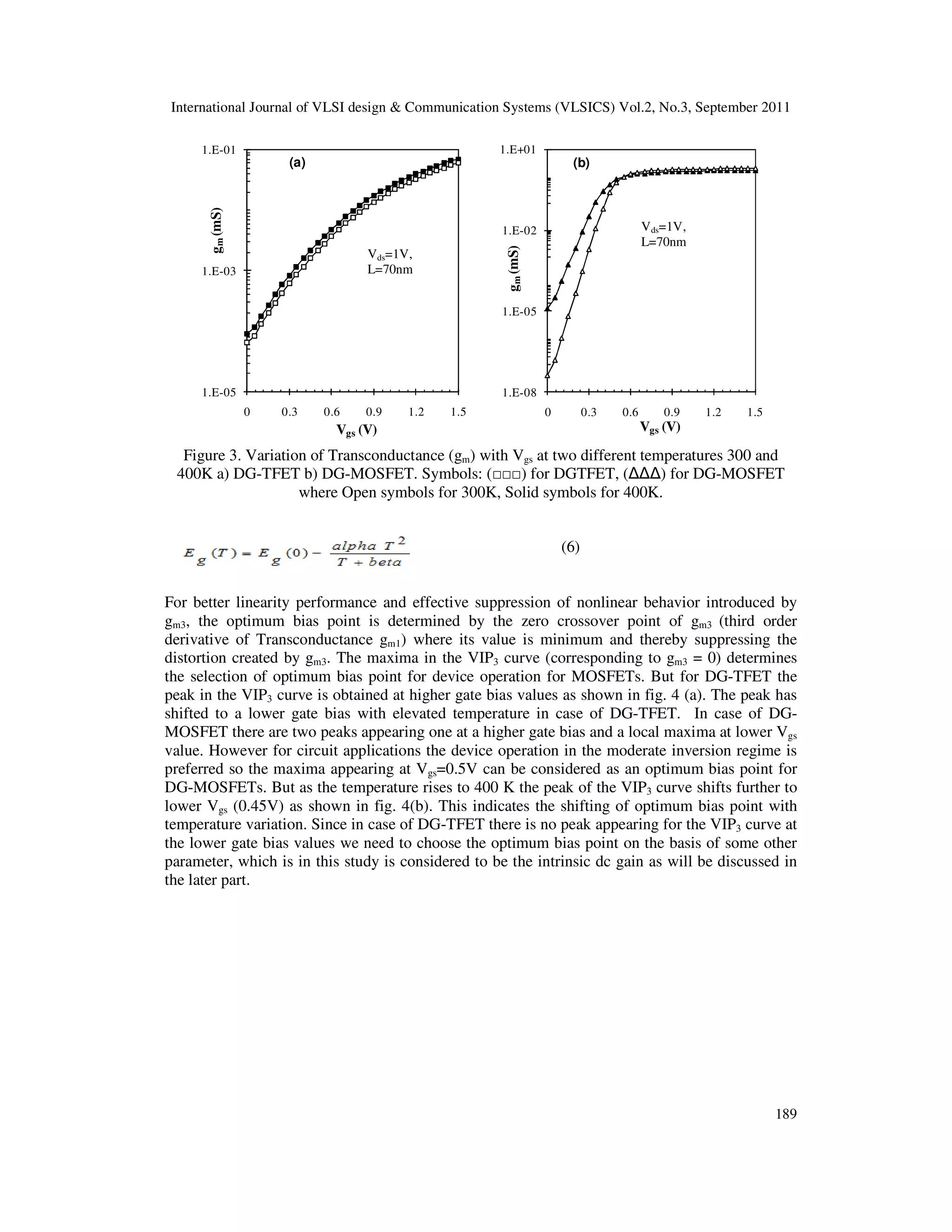
Figure 2 Transfer characteristics (Ids-Vgs) of (a) DG-TFET and (b) DG-MOSFET at two different
temperatures. Symbols: (□□□) for DGTFET, ( ) for DG-MOSFET where Open symbols for
300K, Solid symbols for 400K.
Since the current depends on the band gap which is a function of temperature [16] as modeled in
ATLAS and given by eq. 6, where the default values of alpha and beta are material dependent.
With rise in temperature the band gap value reduces which leads to the increase in the band to
band tunneling current of the DG-TFET.
The reduction in the threshold voltage (Vth) is also minimum in case of DG-TFETs. The threshold
voltage reduces to 0.296 @Vds=1V and T= 400K from its value 0.33V @ Vds=1V and T=300K.
While in case of DG-MOSFET, due to increase in temperature the carriers generated in the
channel increases thus leading to significant reduction of threshold voltage (Vth @ Vds=1V and
T= 400K is 0.22V and Vth @ Vds=1V and T=300K is 0.33V) but the current degrades due to
channel mobility degradation at high temperature arising due to the increased phonon scattering.
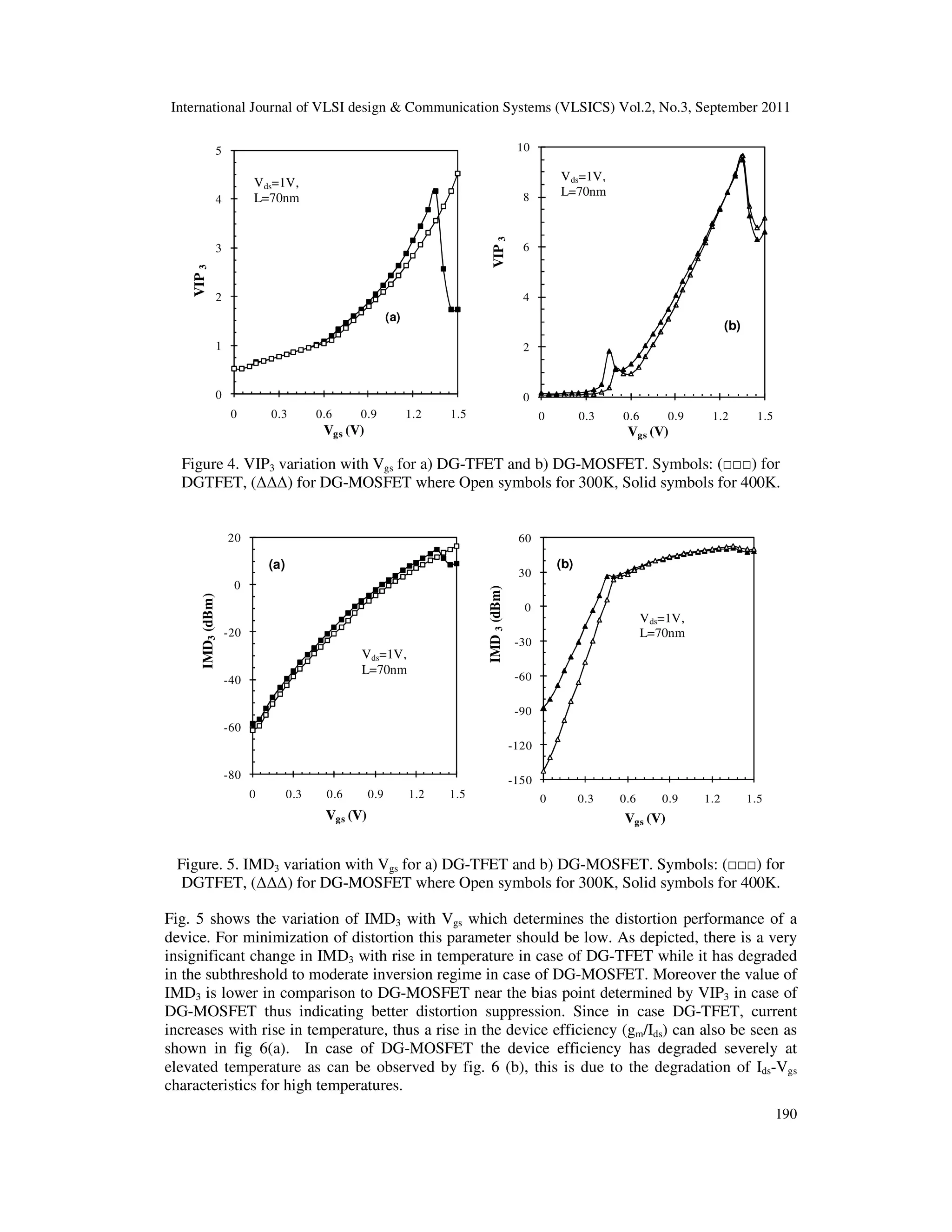
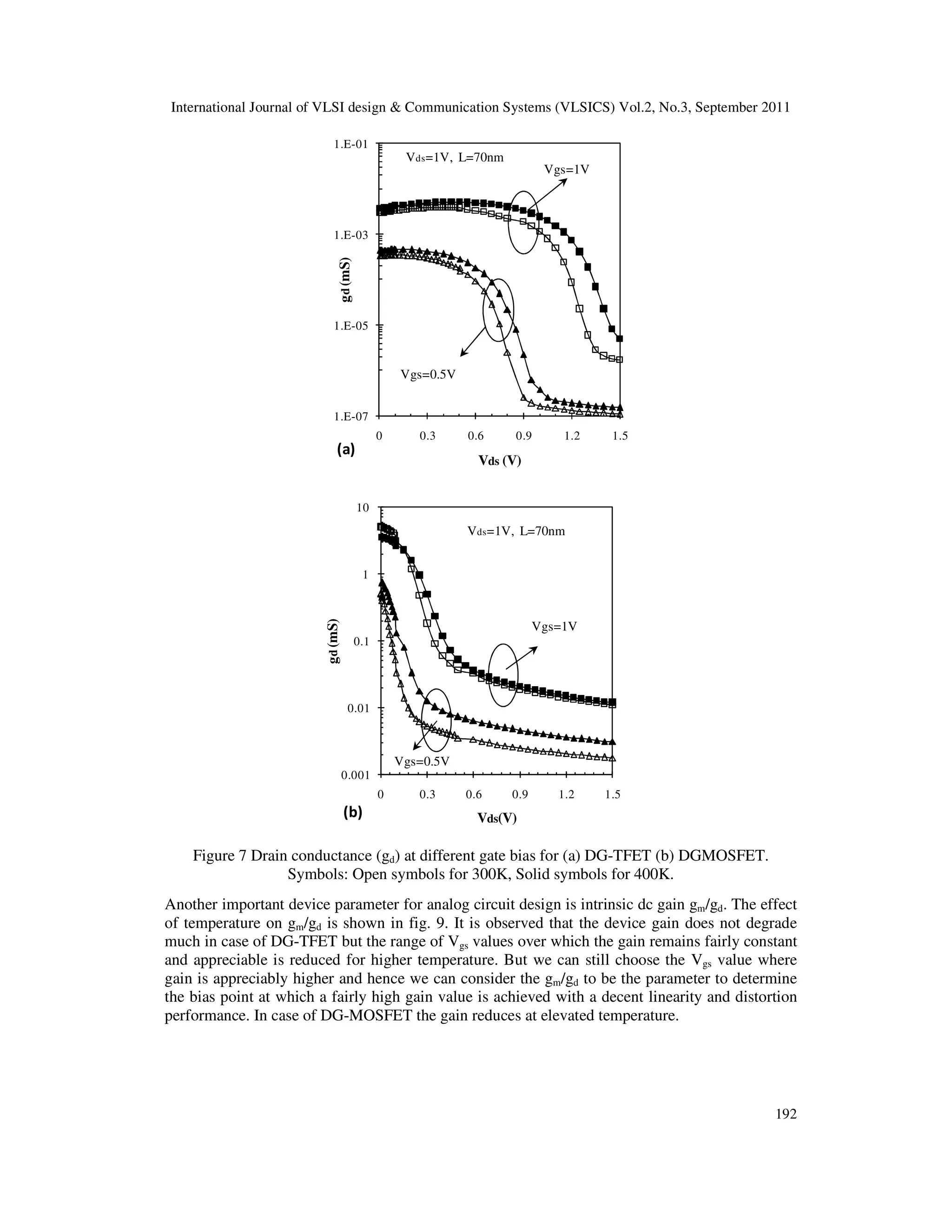
Fig 3 (a) & (b) shows the impact of temperature on the transconductance characteristics of DG-
TFET and DG-MOSFET. As clearly observed there is a very insignificant change in the
magnitude for the case of DG-TFET in contrast with that of DG-MOSFET in which the
transconductance has significantly enhanced only in the subthreshold region due to degraded
subthreshold characteristics of DG-MOSFET at elevated temperatures.](https://image.slidesharecdn.com/2311vlsics16-180705090411/75/LINEARITY-AND-ANALOG-PERFORMANCE-ANALYSIS-OF-DOUBLE-GATE-TUNNEL-FET-EFFECT-OF-TEMPERATURE-AND-GATE-STACK-4-2048.jpg)
![International Journal of VLSI design & Communication Systems (VLSICS) Vol.2, No.3, September 2011
194
1.E+03
1.E+05
1.E+07
0 0.3 0.6 0.9 1.2 1.5
Rout(KΩ)
Vds (V)
Vgs=0.5V
L=70nm
(a)
0
100
200
300
400
500
600
0 0.3 0.6 0.9 1.2 1.5
Rout(KΩ)
Vds (V)
Vgs=0.5V
L=70nm
(b)
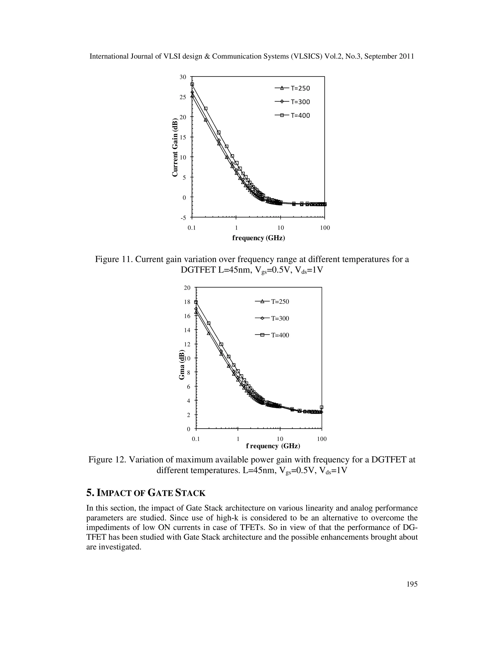
Figure 10. Output resistance (Rout) vs Vds for a) DGTFET b) DGMOSFET. Symbols: (□□□) for
DGTFET, ( ) for DG-MOSFET where Open symbols for 300K, Solid symbols for 400K
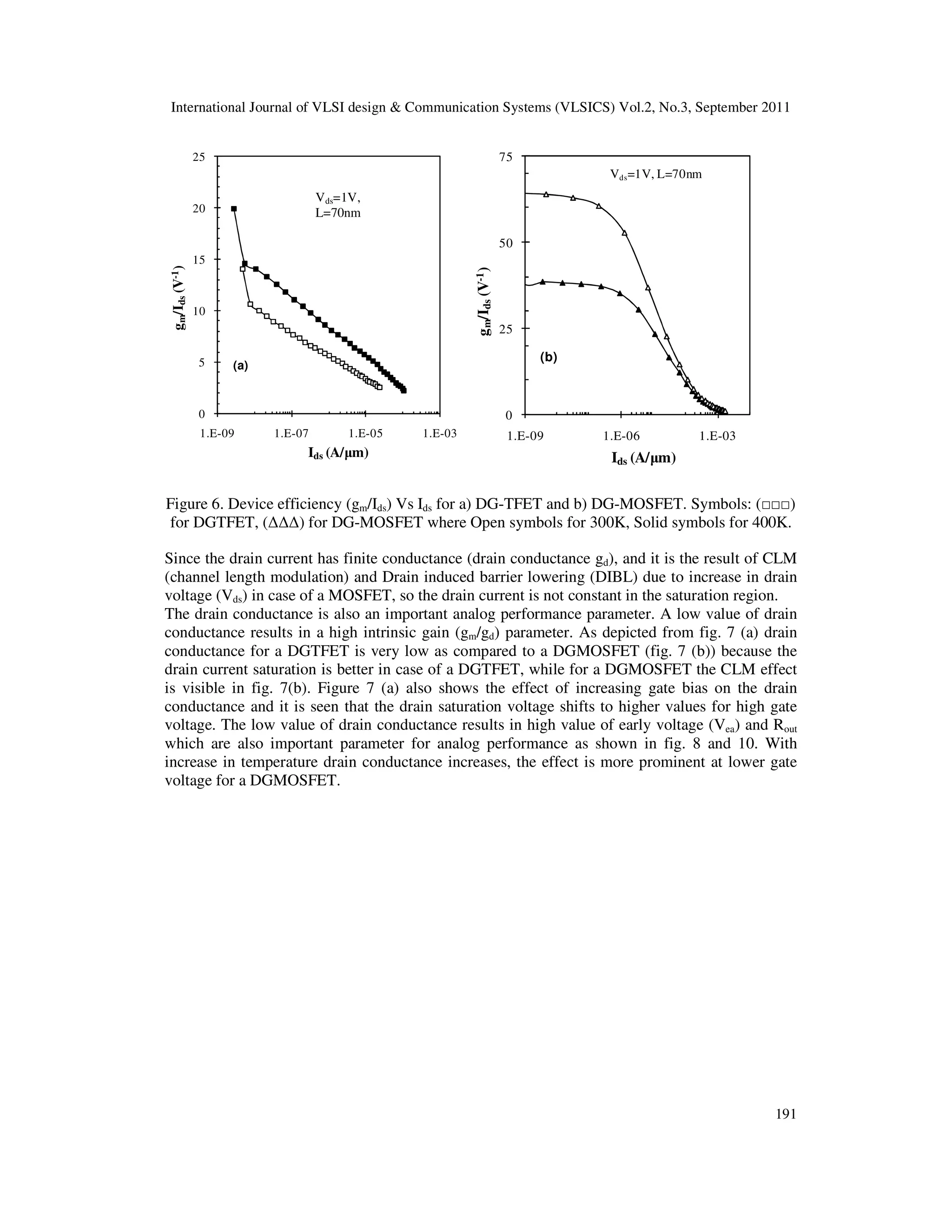
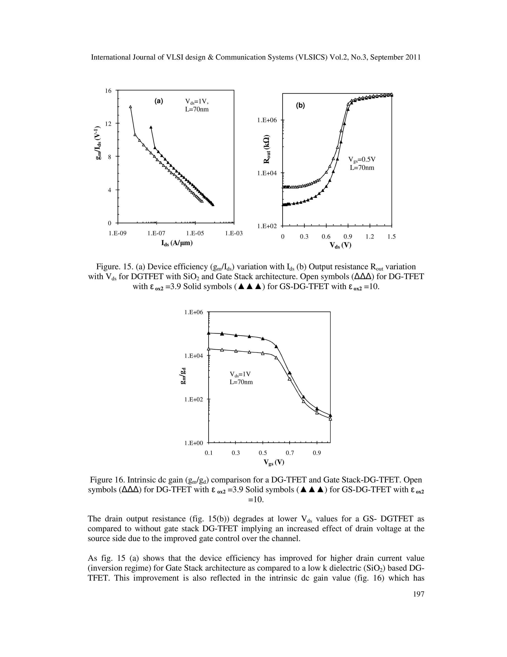
The drain output resistance degrades rapidly for a DG-MOSFET at higher temperature while the
reduction is nominal in case of DG-TFET as shown in fig. 8. Thus DGTFET offers better analog
performance as also predicted in an experimental demonstration of multiple gate TFET [17].
To study the dynamic performance, high frequency ac simulations are carried out in the range of
100MHz to 100 GHz. The parameter Current gain (H21) is extracted and its variation with
frequency is shown in fig. 11. Current gain ( 21
2 ( )
m
gs gd
g
H
f C Cπ
=
+
) depends on trans
conductance (gm) and source, drain parasitic capacitances Cgs and Cgd. With increasing
temperature, drain current increases in case of a TFET and so does transconductance, thus current
gain also increases (fig. 11) and similarly the maximum available power gain also increases
(fig.12). Cut off frequency which is evaluated as that frequency at which the current gain
becomes unity. It also increases, because it directly depends on transconductance. The cut-off
frequencies obtained at gate bias (Vgs=0.5V, Vds=1V) are 1.84GHz, 2GHz and 2.54 GHz at
temperatures 250K, 300K and 400K respectively. At high gate bias (saturation condition,
Vgs=0.7V, Vds=1V), cut off frequencies evaluated for a DGTFET are 4.9GHz, 5.4 and 6.4GHz at
temperatures 250K, 300K and 400K respectively.](https://image.slidesharecdn.com/2311vlsics16-180705090411/75/LINEARITY-AND-ANALOG-PERFORMANCE-ANALYSIS-OF-DOUBLE-GATE-TUNNEL-FET-EFFECT-OF-TEMPERATURE-AND-GATE-STACK-10-2048.jpg)
![International Journal of VLSI design & Communication Systems (VLSICS) Vol.2, No.3, September 2011
198
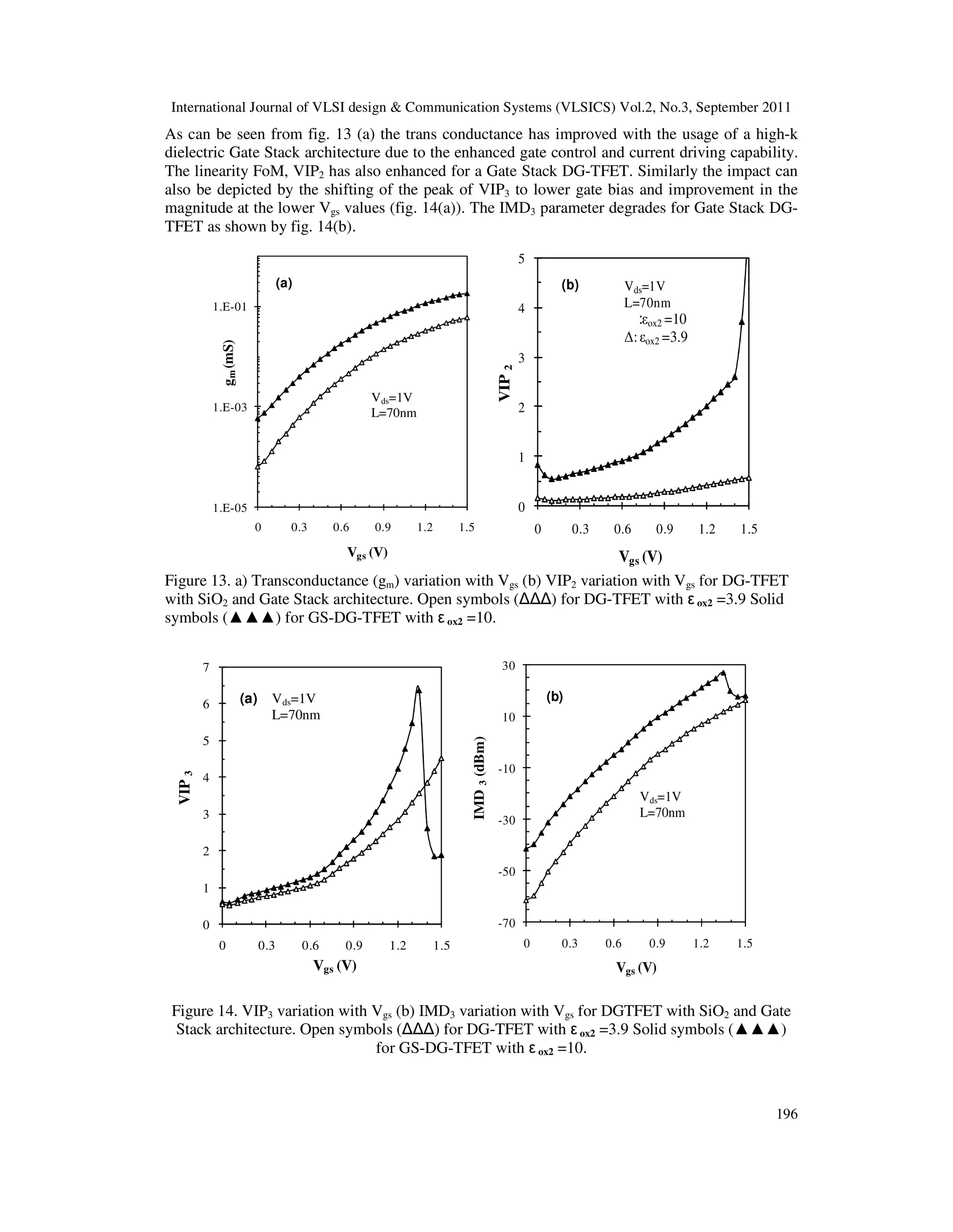
significantly improved for GS-DGTFET. This improvement is due to the enhanced current and
Transconductance (gm) due to the improvement of gate control introduced by gate stack.
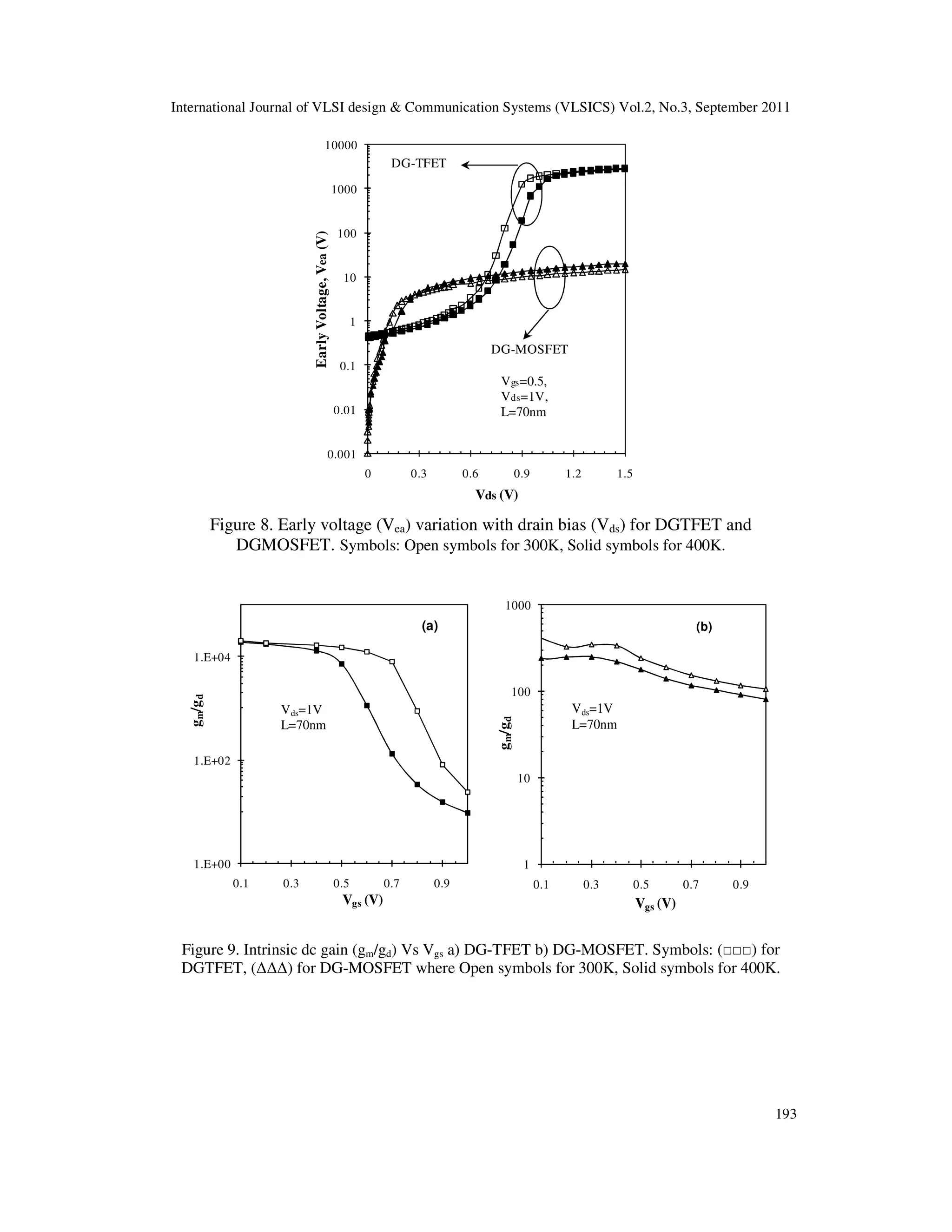
6. CONCLUSIONS
The impact of temperature variation and introduction of Gate Stack architecture on the linearity
and analog performance of a DG-TFET has been studied. It has been shown that TFETs are more
immune to temperature variations in terms of its stable bias point selection based on achieving
high dc gain value, which is an advantage as compared to DG-MOSFET in which the bias point
chosen varies with temperature variations. The suppression of distortion is better in case of DG-
TFET as compared to DG-MOSFET and they also offer a high drain output resistance (due to a
lower DIBL effect), early voltage and intrinsic dc gain which does not significantly degrade even
at high temperature range. Further improvement in terms of linearity and higher gain can also be
obtained by using Gate Stack architecture.
ACKNOWLEDGEMENTS
Author (Rakhi Narang) would like to thank University Grants Commission (UGC), Government
of India, for financially supporting this research work.
REFERENCES
[1] B. Nauta, and A-J. Annema, (2005) “Analog/RF Circuit Design Techniques for Nanometerscale IC
Technologies”, Proceedings of 31st European Solid-State Circuits Conference, ESSCIRC, pp. 45-53.
[2] Q. Zhang, and A. Seabaugh, (2008) “Can the Interband Tunnel FET Outperform Si CMOS?”,
Proceedings of Device Research Conference, pp. 73-74.
[3] S. H. Kim, H. Kam, C. Hu, and T- J. K. Liu, (2009) “Germanium-source tunnel field effect transistors
with record high ION/IOFF”, Symposium on VLSI Technology, pp. 178 – 179.
[4] W. Y. Choi, B. G. Park, J. D. Lee and T. K. Liu, (2007) “Tunneling field effect transistors (TFETs)
with subthreshold swing (SS) less than 60 mV/dec”, IEEE Electron Device Lett., vol. 28, pp. 743–
745.
[5] S. Mookerjea, and S.Datta, (2008) “Comparative study of Si, Ge and InAs based steep subthreshold
slope tunnel transistors for 0.25V supply voltage logic applications”, Proceedings of 63rd Device
Research Conference, pp. 47–48.
[6] M. Born, K.K. Bhuwalka, M. Schindler, U. Abilene, M. Schmidt, T. Sulima, and I. Eisele,
(2006) “Tunnel FET: A CMOS Device for high Temperature Applications”, 25th International
Conference on Microelectronics, pp. 124-127.
[7] P-F. Guo, L-T. Yang, Y. Yang, L. Fan, G-Q. Han, G.S. Samudra, and Y-C. Yeo, (2009) “Tunneling
Field-Effect Transistor: Effect of Strain and Temperature on Tunneling Current”, IEEE Electron
Device Letters, Vol. 30, pp. 981 – 983.
[8] J. Wan, C. L.Royer, A. Zaslavsky, and S. Cristoloveanu, (2010) “SOI TFETs: Suppression of
ambipolar leakage and low-frequency noise behavior”, Proceedings of the European Solid-State
Device Research Conference (ESSDERC), pp: 341 – 344.
[9] T. Nirschl, P-F. Wang, W. Hansch, and D. Schmitt-Landsiedel, (2004) “The tunneling field effect
transistors (TFET): the temperature dependence, the simulation model, and its application”,
Proceedings of the 2004 International Symposium on Circuits and Systems, pp. 713-16.
[10] C. Anghel, P.Chilagani, A. Amara, and A. Vladimirescu, (2010) “Tunnel field effect transistor with
increased ON current, low-k spacer and high-k dielectric”, Applied Physics Letters, 96, pp. 122104.](https://image.slidesharecdn.com/2311vlsics16-180705090411/75/LINEARITY-AND-ANALOG-PERFORMANCE-ANALYSIS-OF-DOUBLE-GATE-TUNNEL-FET-EFFECT-OF-TEMPERATURE-AND-GATE-STACK-14-2048.jpg)
![International Journal of VLSI design & Communication Systems (VLSICS) Vol.2, No.3, September 2011
199
[11] K. Boucart, A. M. Ionescu, (2007) “Double-gate tunnel FET with high- k gate dielectric”, IEEE
Trans. Electron Devices, Vol. 54, no. 7, pp. 1725–1733.
[12] ATLAS Device Simulation Software, Silvaco Int., Version 5.14.0.R
[13] P.H. Woerlee, M.J. Knitel, R. van Langevelde, D.B.M. Klaassen, L.F. Tiemeijer, A.J. Scholten, and
A.T.A. Zegers-van Duijnhoven, (2001) “RF-CMOS performance trends”, IEEE Transactions on
Electron Devices, Vol 48, 8, pp. 1776 – 1782.
[14] W. Ma, and S.Kaya, (2003) “Study of RF Linearity in sub-50nm MOSFETs using Simulations”,
Journal of Computational Electronics 2, pp. 347-352.
[15] S. Kaya, W. Ma, and A. Asenov, (2003) “Design of DG-MOSFETs for High Linearity Performance”
IEEE International SOI Conference, pp. 68-69.
[16] S. M. Sze: Physics of Semiconductor Devices (Wiley, New York, 1981).
[17] M. Fulde, A. Heigl, M. Weis, M. Wimshofer, K. V. Arnim, T. Nirschl, M. Sterkel, G.
Knoblinger, W. Hansch, G. Wachutka, and D.Schmitt-Landsiedel, (2008)
”Fabrication, Optimization and Application of Complementary Multiple-Gate Tunneling FETs”,
Proceeddings of IEEE International Nanoelectronics Conference (INEC), pp. 579 – 84.
Authors
Rakhi Narang received B.Sc. degree in electronics from University of Delhi in Year 2005
and received the Master’s degree from Department of Electronic Science, University of
Delhi, South Campus New Delhi, in year 2007. She is currentl y a research fellow and
working towards the Ph. D. Degree at Department of Electronic Science, University of
Delhi, South Campus. Her research interests include Modelling and Simulation of novel
device architectures like Tunnel Field Effect Transistor.
Manoj Saxena is Assistant Professor in Department of Electronics, Deen dayal
Upadhyaya College, University of Delhi, New Delhi, India. He received B.Sc. (with
honors), M. Sc., and Ph.D. degrees from the University of Delhi, New Delhi, in 1998,
2000, and 2006, respectively, all in electronics. He joined Department of Electronics,
Deen Dayal Upadhyaya College, University of Delhi in 2000. He is the Co-principal
Investigator in research project sponsored by DRDO, Govt. of India and University
Grants Commission (UGC), Govt. of India. He has authored or coauthored 119 technical
papers in inte rnational journals and various international and national conferences. He
has contributed one chapter entitled MOSFET Modeling in the Encyclopedia on RF and
Microwave Engineering (New York: Wiley, 2005). His current research interests are in
the areas of analytical modeling, design, and simulation of Optically controlled MESFET/MOSFET, silicon-on-
nothing, insulated-shallow-extension, grooved/concave-gate MOSFETs, cylindrical gate MOSFET and Tunnel
FET. Dr. Saxena has reviewed extensively for IEEE TRANSACTIONS ON ELECTRON DEVICES,
Semiconductor Science Technology, Solid State Electronics, Journal of Physics: D Applied Physics,
Superlattices and Microstructures, Elsevier Science, UK, International Journal of Numerical Modeling:
Electronic Networks, Devices and Fields, Wiley, Journal of Electrical and Electronics Engineering Research
(JEEER), MAPAN-Journal of Metrology Society of India and International Journal of Science and Technology
Education Research. His name appeared in the Golden List of IEEE TRANSACTIONS ON ELECTRON
DEVICES Reviewers since 2005. He is also listed in the 25th Anniversary edition of Who’s Who in the World.
He is Member of Institute of Physics (IOP), UK and Senior Member-IEEE (USA). He is Member of National
Academy of Sciences India (NASI), Allahabad, India, Institution of Engineering and Technology (IET), UK,
and International Association of Engineers, Hong Kong, Life Member of Semiconductor Society of India, New
Delhi, India, Life Member of Indian Science Congress Association (ISCA), Young Associate of Indian Academy
of Sciences (IAS), Bangalore, India and Joint Secretary of Society for VLSI and Microelectronics, New Delhi,
India and Secretary of IEEE EDS Delhi Chapter, New Delhi](https://image.slidesharecdn.com/2311vlsics16-180705090411/75/LINEARITY-AND-ANALOG-PERFORMANCE-ANALYSIS-OF-DOUBLE-GATE-TUNNEL-FET-EFFECT-OF-TEMPERATURE-AND-GATE-STACK-15-2048.jpg)

The study investigates the linearity and analog performance of silicon double gate tunnel field effect transistors (DG-TFET) and the effect of temperature and gate stack architecture on their performance. It finds that DG-TFET demonstrates better resilience to temperature changes compared to DG-MOSFET, exhibiting minimal performance degradation and improved efficiency, particularly in analog applications. Simulations reveal the impact of temperature on key performance metrics like transconductance and distortion, highlighting the advantages of DG-TFET for future communication technologies.