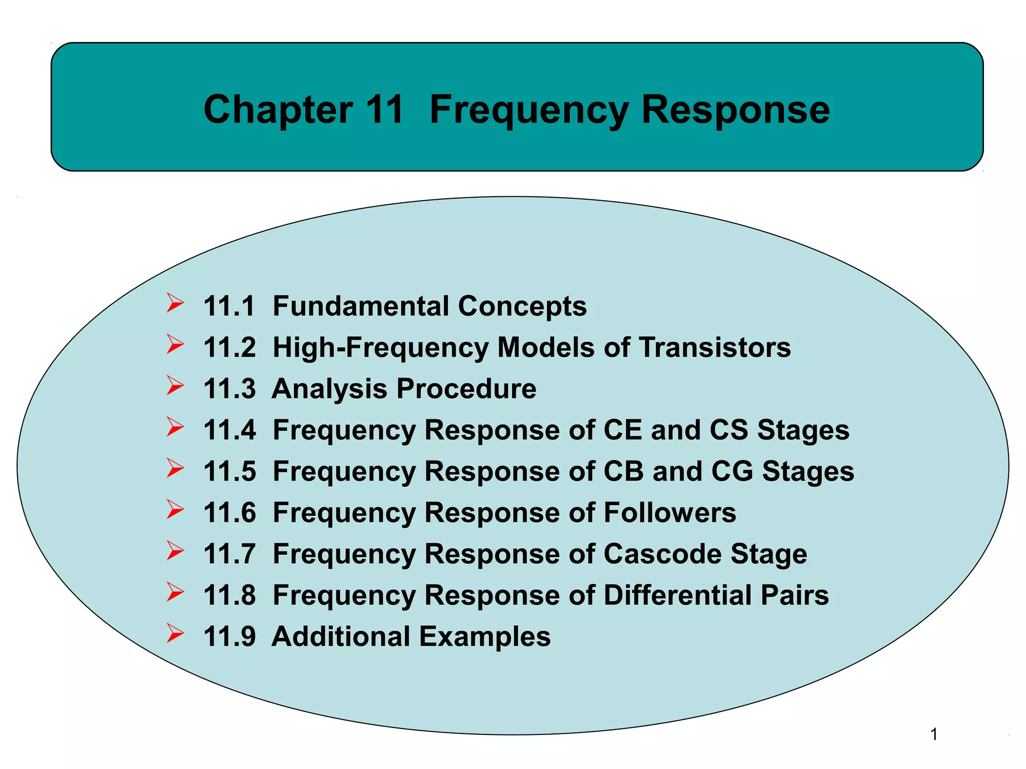
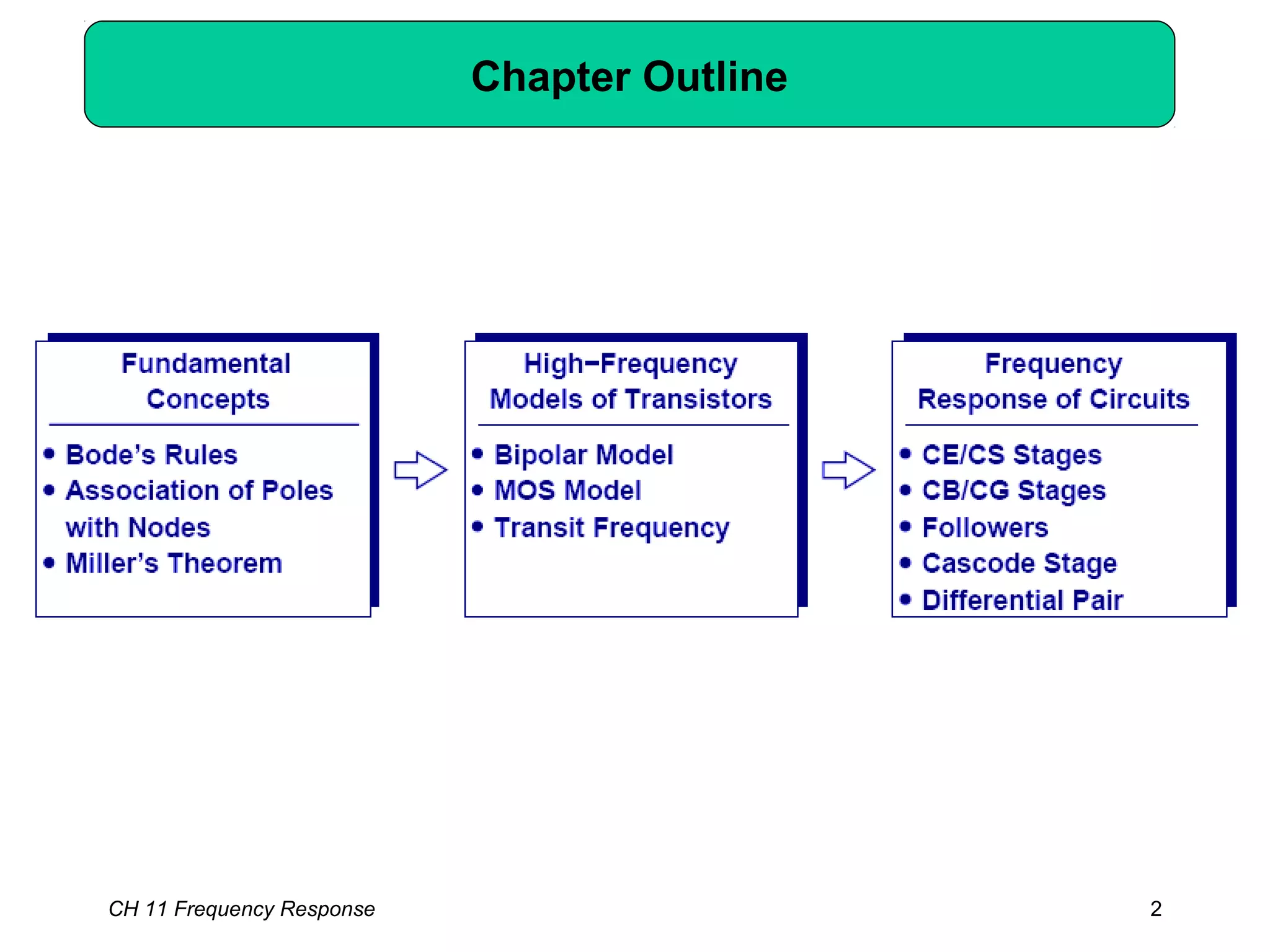
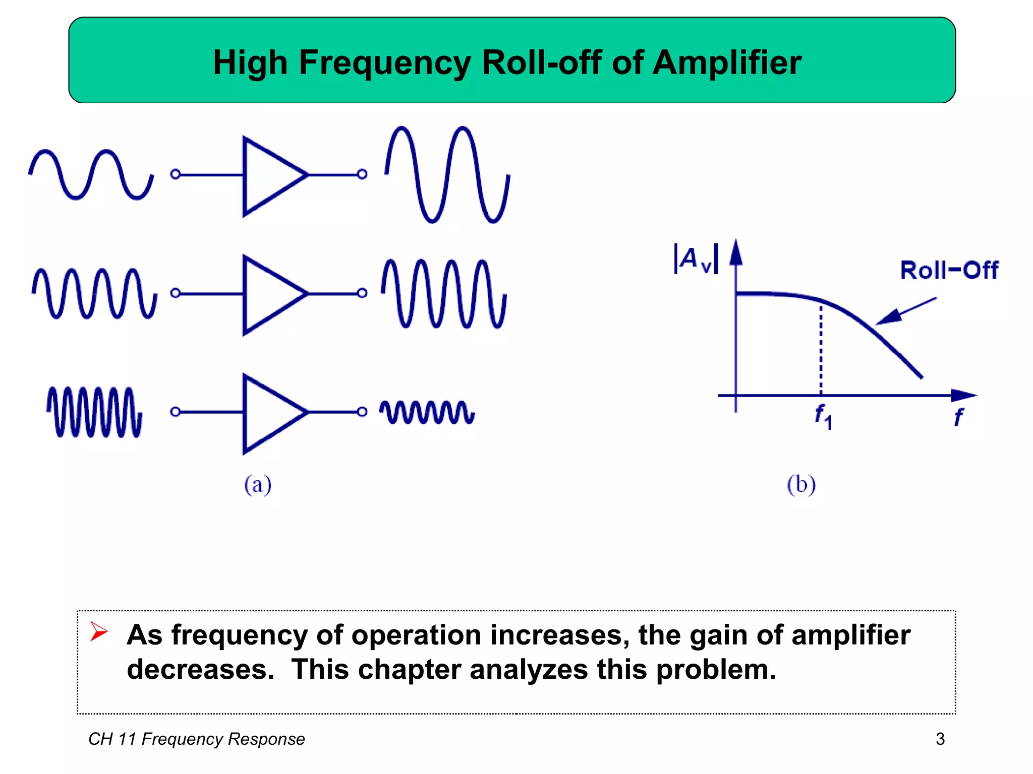
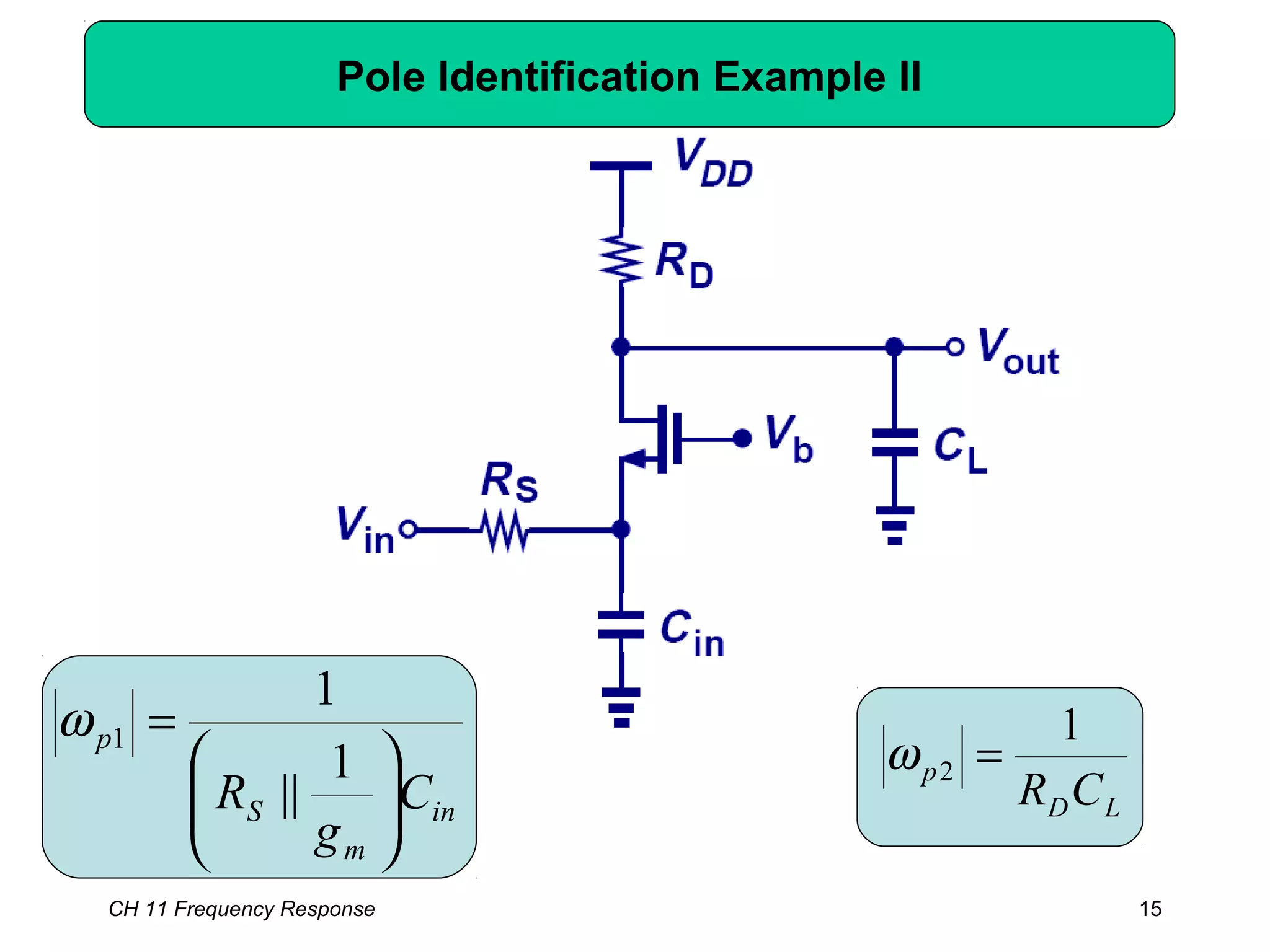
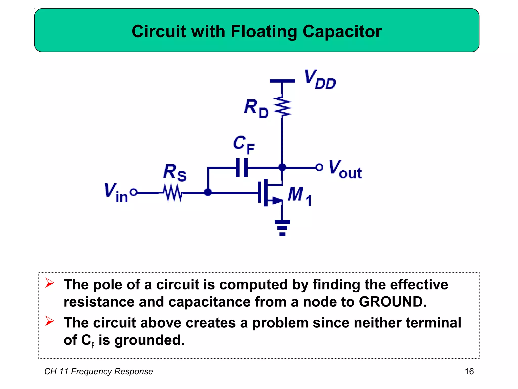
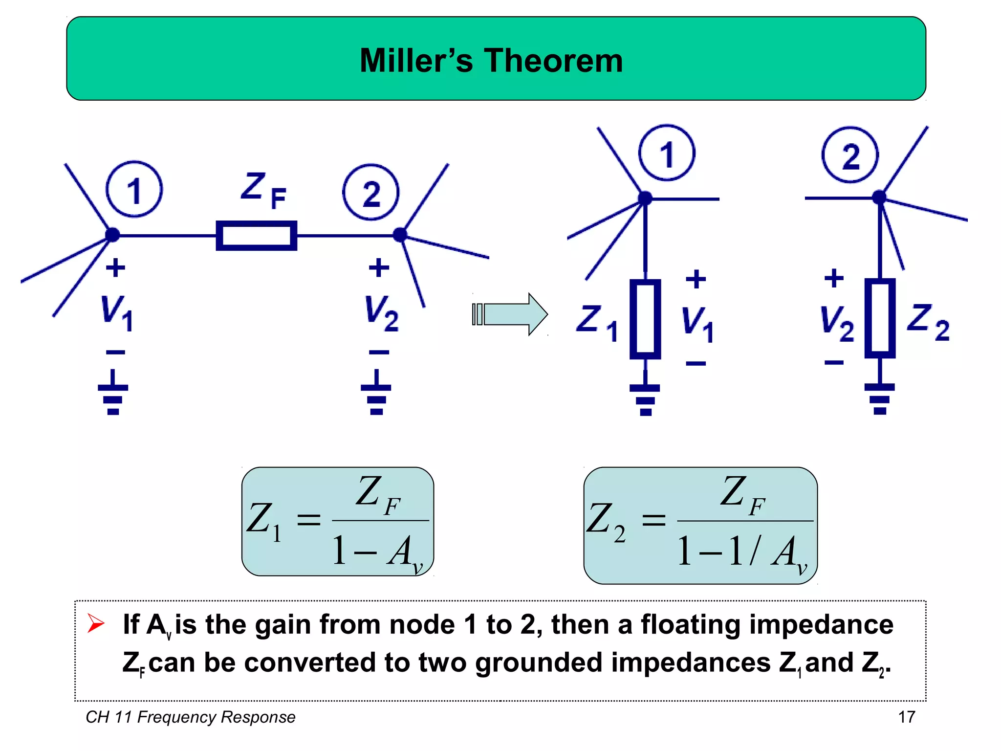
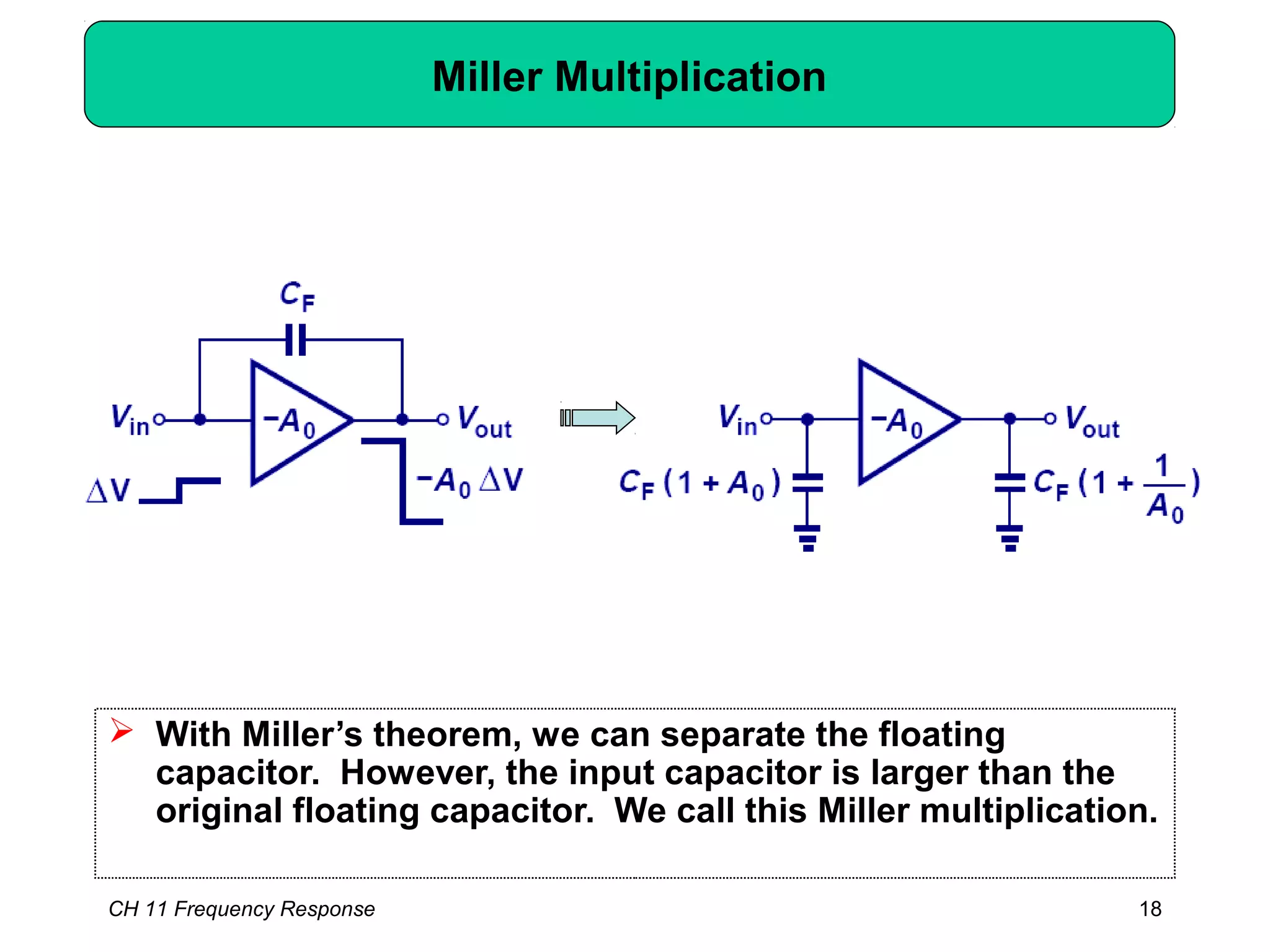
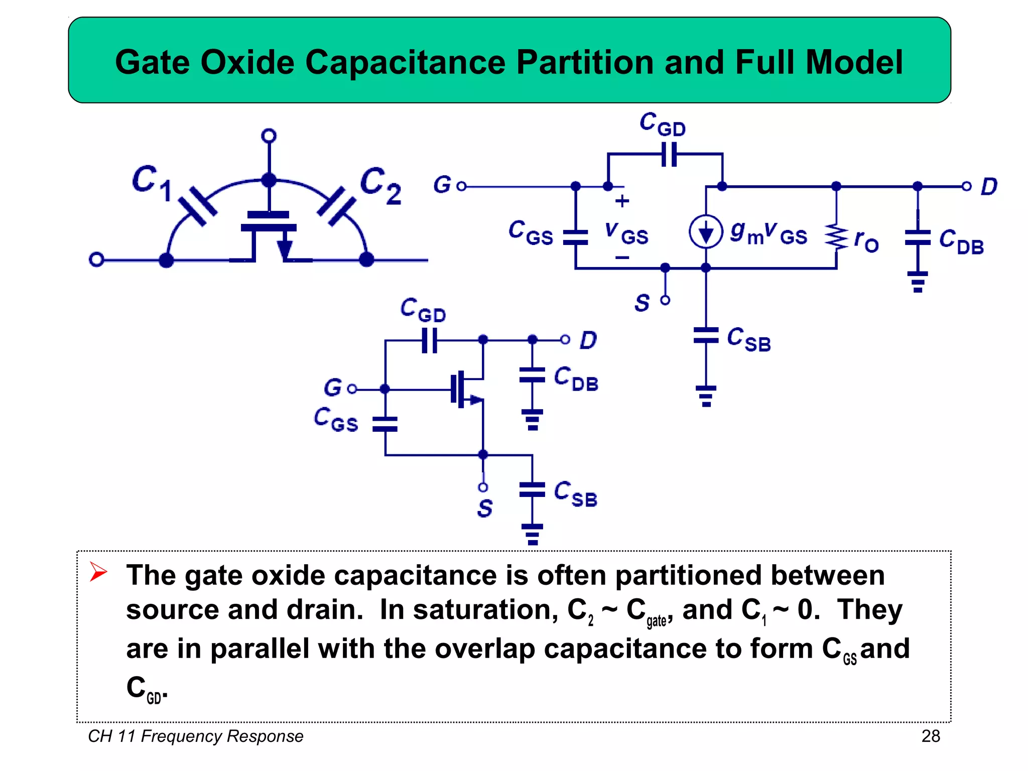
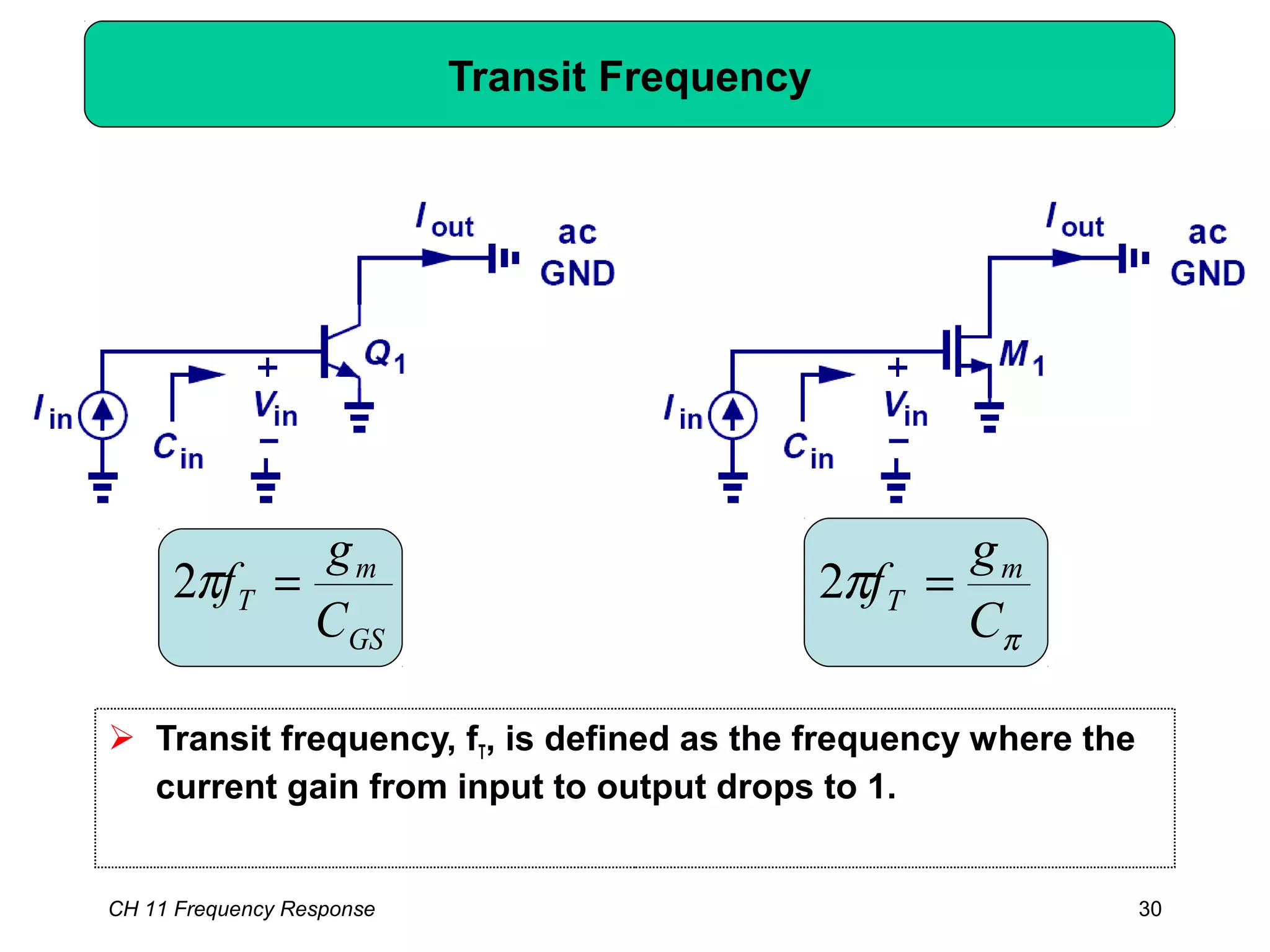
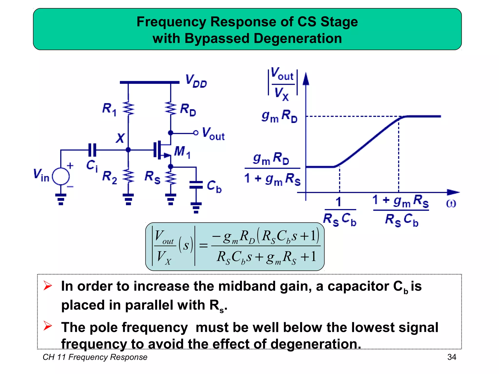
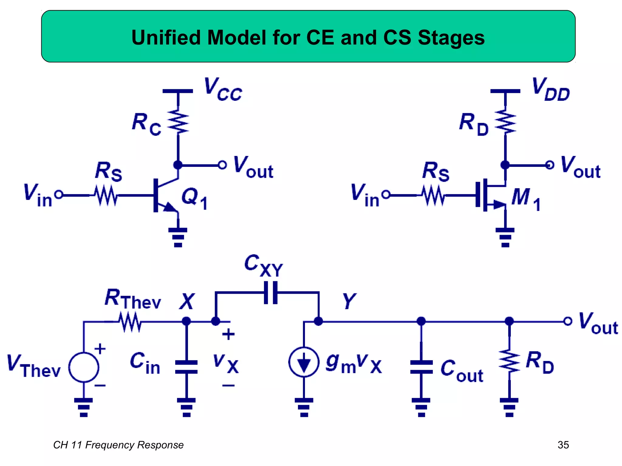
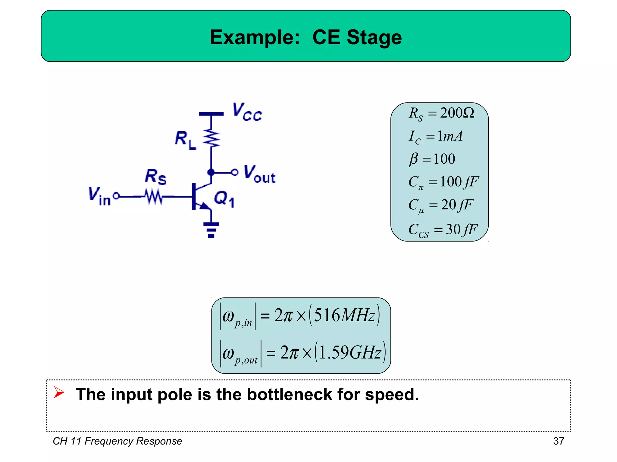
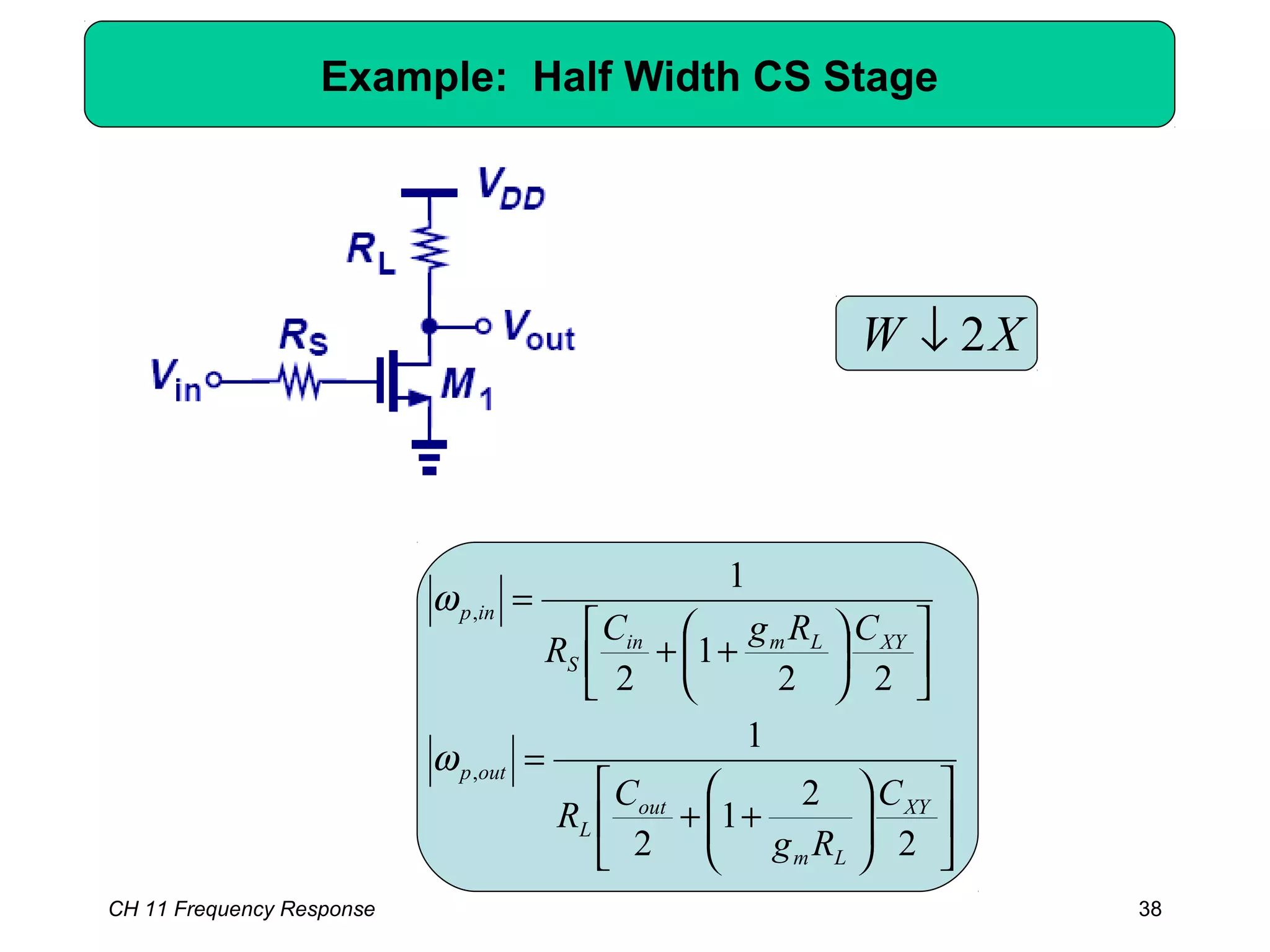
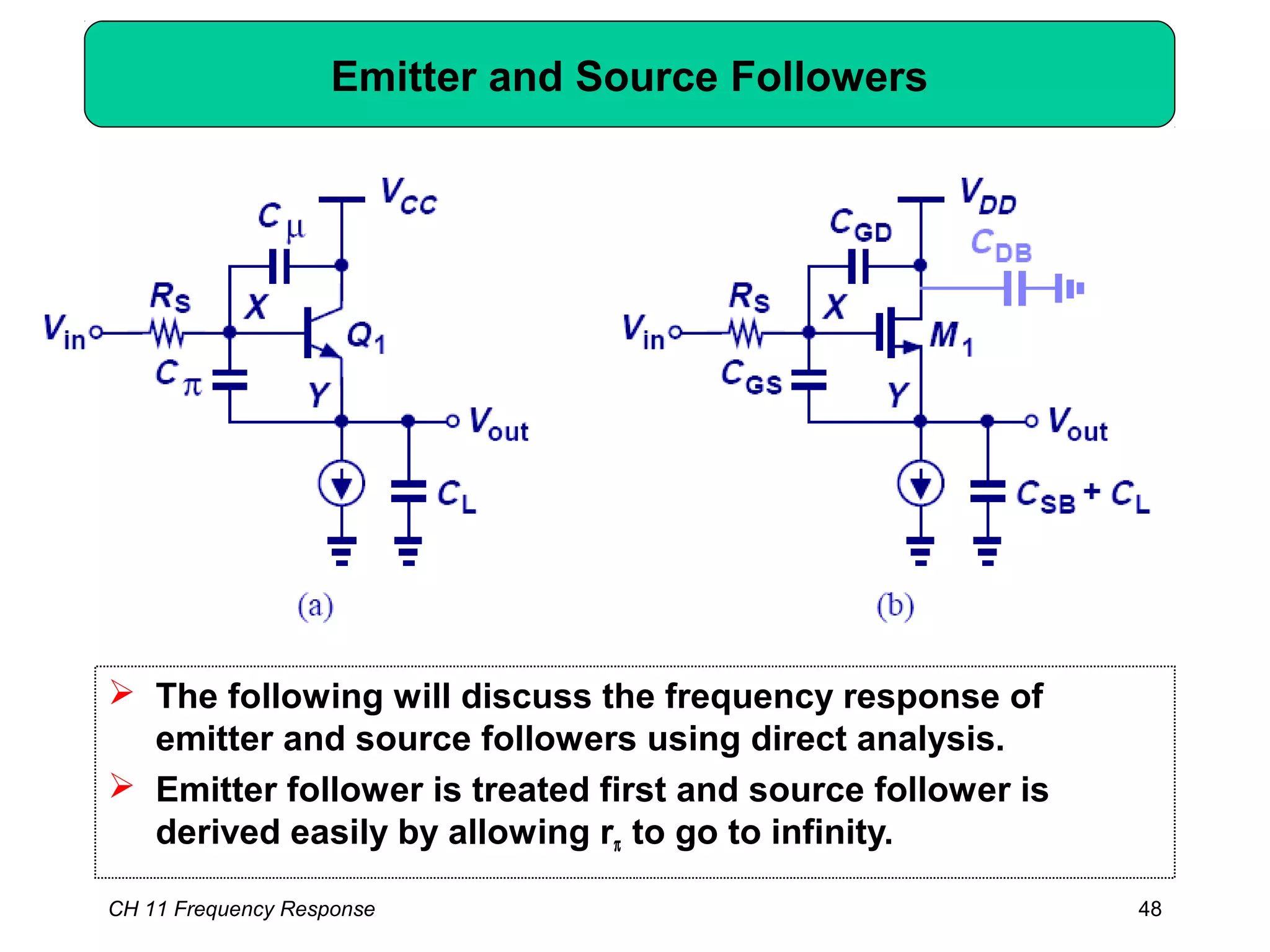
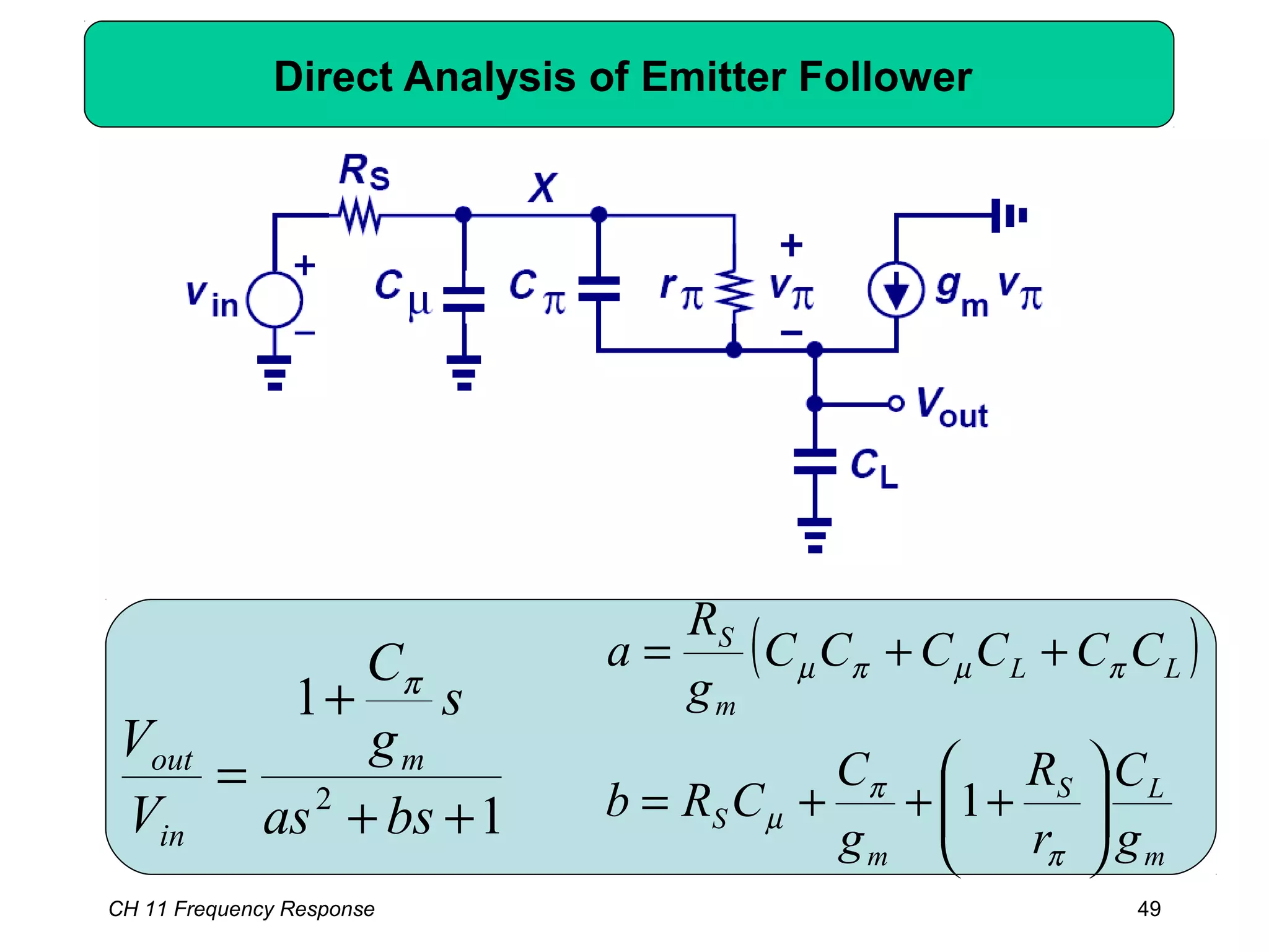
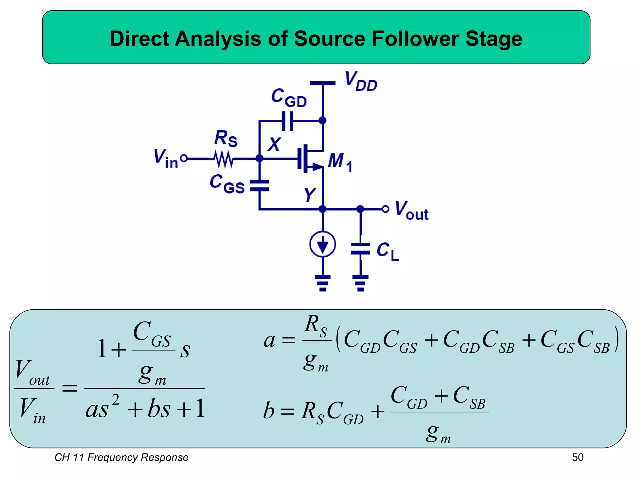
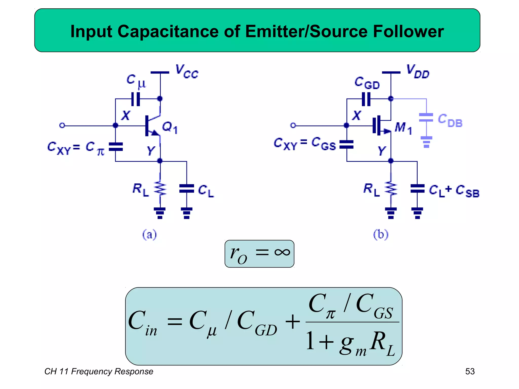
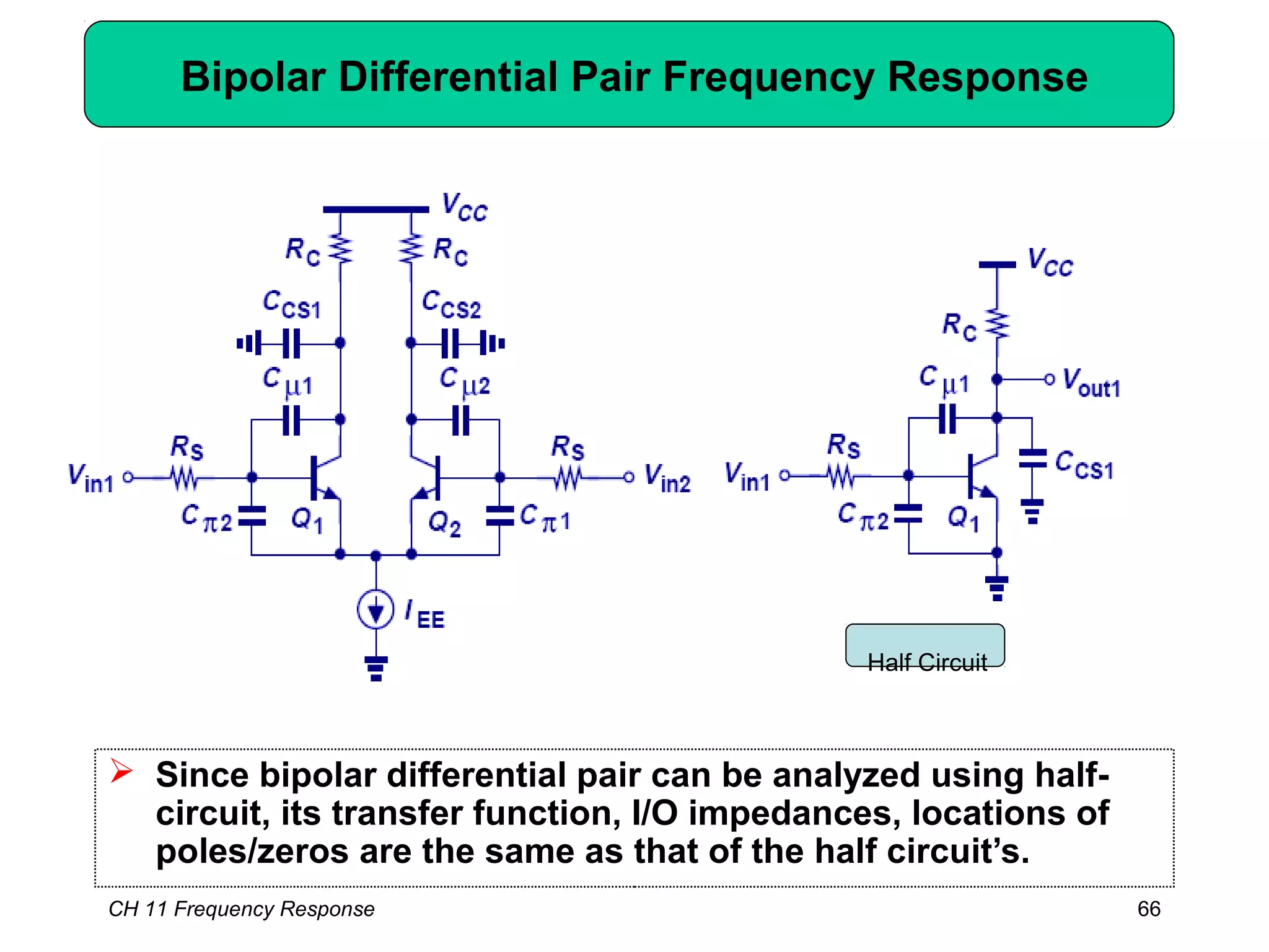
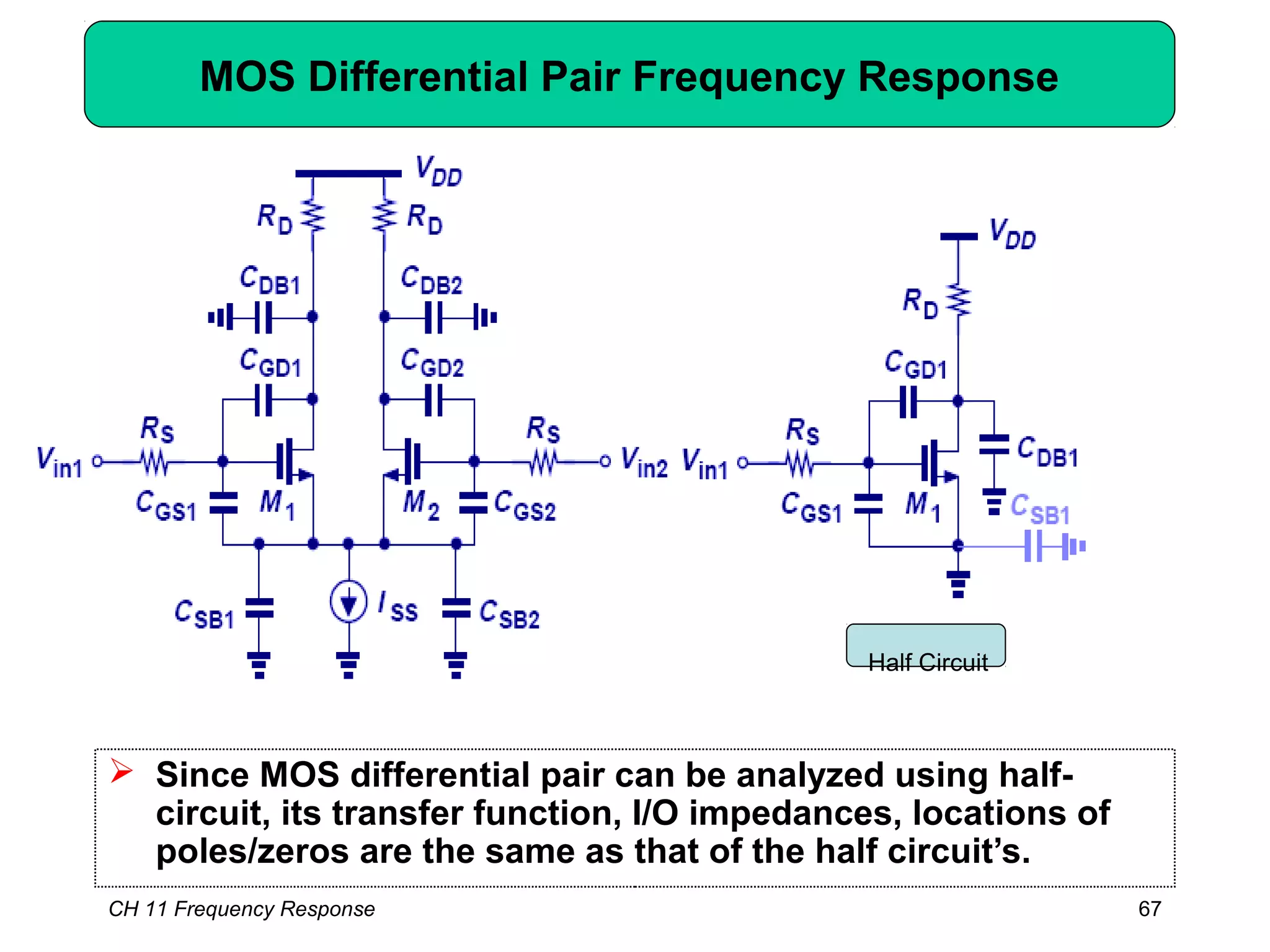
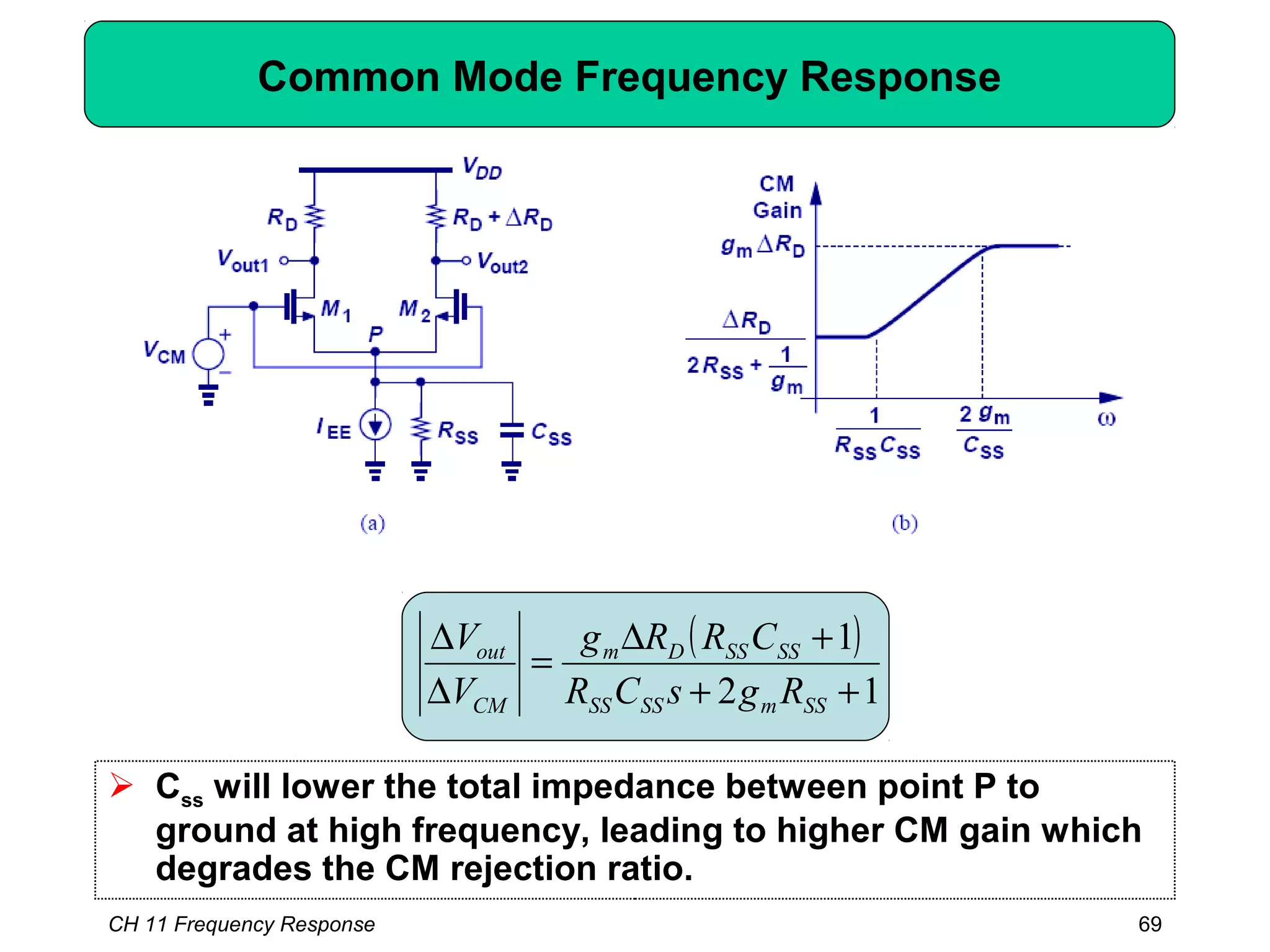
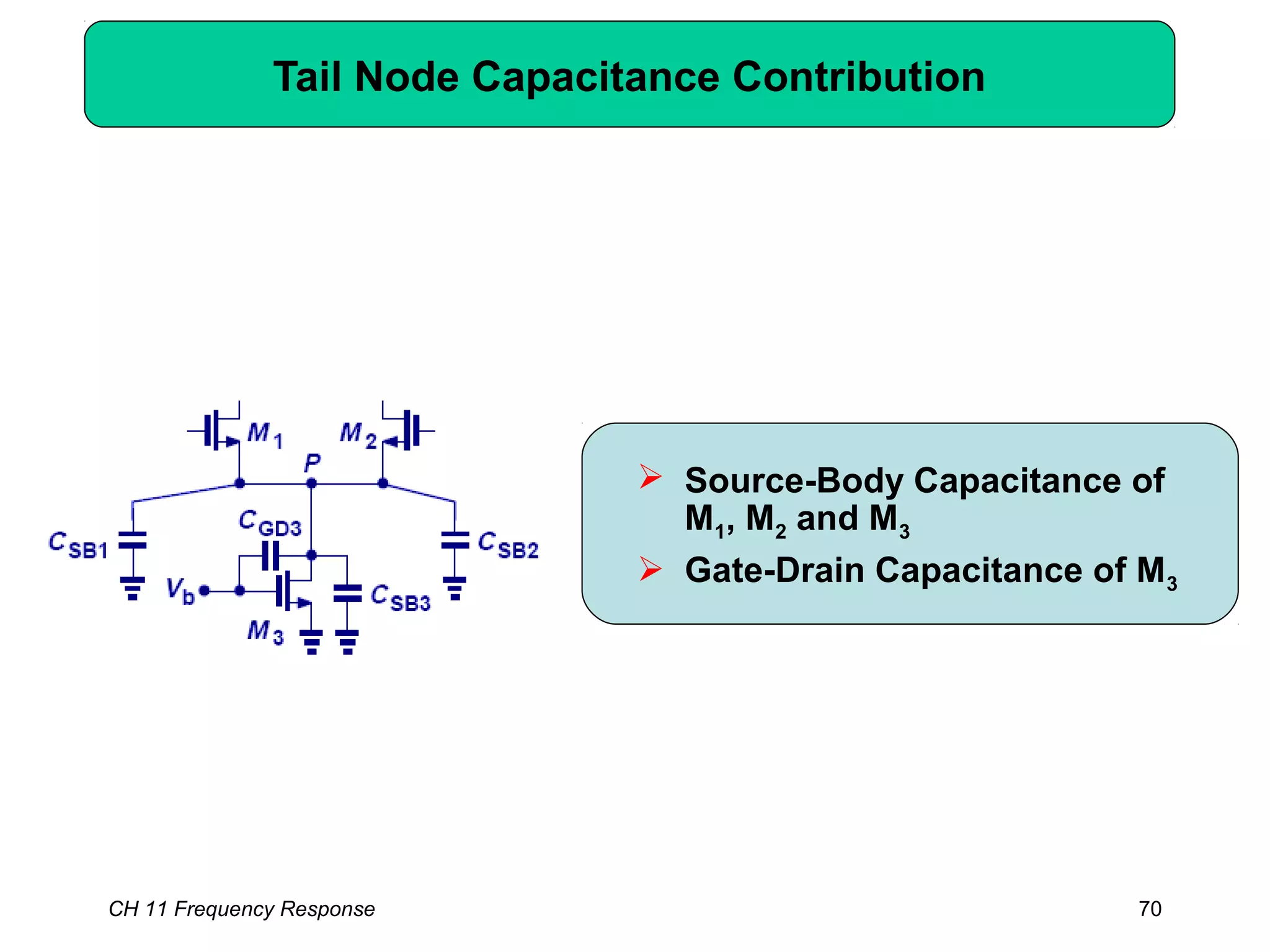
This chapter discusses the frequency response of amplifiers. It begins with fundamental concepts and high-frequency models of transistors. It then analyzes the frequency response of common emitter, common source, common base, and common gate stages. Additional topics covered include frequency response of followers, cascode stages, differential pairs, and more examples. Analysis methods like Bode plots, pole identification, and Miller's theorem are explained. Key factors that influence frequency response like bandwidth, gain rolloff, and various transistor capacitances are also analyzed.


![CH 11 Frequency Response 40
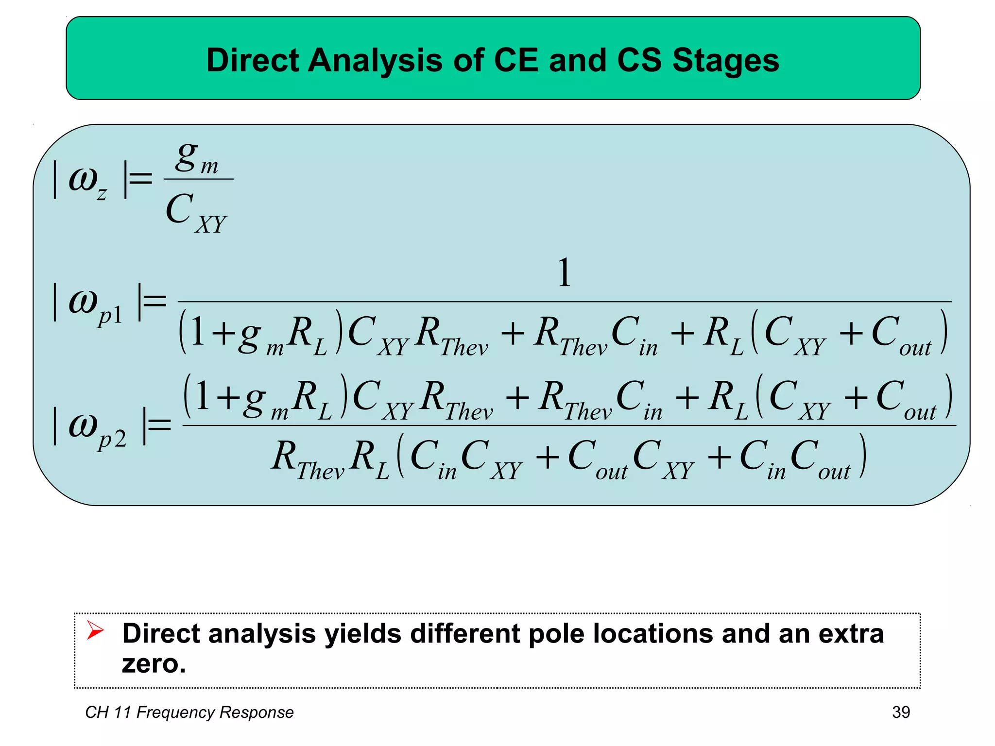
Example: CE and CS Direct Analysis
( )[ ] ( )
( )[ ] ( )
( )( )outinXYoutXYinOOS
outXYOOinSSXYOOm
p
outXYOOinSSXYOOm
p
CCCCCCrrR
CCrrCRRCrrg
CCrrCRRCrrg
++
++++
≈
++++
≈
21
21211
2
21211
1
||
)(||||1
)(||||1
1
ω
ω](https://image.slidesharecdn.com/frequencyresponse-150520175424-lva1-app6892/75/Frequency-response-40-2048.jpg)
![CH 11 Frequency Response 42
Input Impedance of CE and CS Stages
( )[ ] π
µπ
r
sCRgC
Z
Cm
in ||
1
1
++
≈
( )[ ]sCRgC
Z
GDDmGS
in
++
≈
1
1](https://image.slidesharecdn.com/frequencyresponse-150520175424-lva1-app6892/75/Frequency-response-42-2048.jpg)


![Example: Frequency Response of Source Follower
( )
0
150
100
80
250
100
200
1
=
Ω=
=
=
=
=
Ω=
−
λ
m
DB
GD
GS
L
S
g
fFC
fFC
fFC
fFC
R
( )[ ]
( )[ ]GHzjGHz
GHzjGHz
p
p
57.279.12
57.279.12
2
1
−−=
+−=
πω
πω
CH 11 Frequency Response 51](https://image.slidesharecdn.com/frequencyresponse-150520175424-lva1-app6892/75/Frequency-response-51-2048.jpg)
![CH 11 Frequency Response 52
Example: Source Follower
1
1
2
++
+
=
bsas
s
g
C
V
V m
GS
in
out
[ ]
1
2211
1
2211111
1
))((
m
DBGDSBGD
GDS
DBGDSBGSGDGSGD
m
S
g
CCCC
CRb
CCCCCCC
g
R
a
+++
+=
++++=](https://image.slidesharecdn.com/frequencyresponse-150520175424-lva1-app6892/75/Frequency-response-52-2048.jpg)


![CH 11 Frequency Response 68
Example: MOS Differential Pair
( )33
,
1
1
3
31
3
,
1311
,
1
1
1
1
])/1([
1
GDDBL
outp
GD
m
m
GSDB
m
Yp
GDmmGSS
Xp
CCR
C
g
g
CC
g
CggCR
+
=
+++
=
++
=
ω
ω
ω](https://image.slidesharecdn.com/frequencyresponse-150520175424-lva1-app6892/75/Frequency-response-68-2048.jpg)
![Example: Capacitive Coupling
( )[ ]EBin RrRR 1|| 222 ++= βπ
( )
( )Hz
CRr B
L 5422
||
1
111
1 ×== πω
π ( )
( )Hz
CRR inC
L 9.22
1
22
2 ×=
+
= πω
CH 11 Frequency Response 71](https://image.slidesharecdn.com/frequencyresponse-150520175424-lva1-app6892/75/Frequency-response-71-2048.jpg)


![Circuit Network Analysis - [Chapter5] Transfer function, frequency response, ...](https://cdn.slidesharecdn.com/ss_thumbnails/ch5-150613063859-lva1-app6891-thumbnail.jpg?width=640&height=640&fit=bounds)