Development of an Algorithm for 16-Bit WTM
•
0 likes•109 views

IOSR Journal of Electronics and Communication Engineering (IOSR-JECE) vol.10 issue.1 version.3
![Development of an Algorithm for 16-Bit WTM
DOI: 10.9790/2834-10137986 www.iosrjournals.org 80 | Page
Wallace tree multiplier reduction stages for 8X8 multiplication [1]](data:image/gif;base64,R0lGODlhAQABAIAAAAAAAP///yH5BAEAAAAALAAAAAABAAEAAAIBRAA7)
Recommended
Recommended
More Related Content
What's hot
What's hot (18)
Viewers also liked
Viewers also liked (20)
Similar to Development of an Algorithm for 16-Bit WTM
Similar to Development of an Algorithm for 16-Bit WTM (20)
More from IOSR Journals
Recently uploaded
Recently uploaded (20)
Development of an Algorithm for 16-Bit WTM
- 1. IOSR Journal of Electronics and Communication Engineering (IOSR-JECE) e-ISSN: 2278-2834,p- ISSN: 2278-8735.Volume 10, Issue 1, Ver. III (Jan - Feb. 2015), PP 79-86 www.iosrjournals.org DOI: 10.9790/2834-10137986 www.iosrjournals.org 79 | Page Development of an Algorithm for 16-Bit WTM 1 Sravanthi.kantamaneni, Asst Professor, 2 Dr.V.V.K.D.V.Prasad, Professor, 3 Veera Vasantha Rao.Battula, Asst. Professor Abstract: Binary Multipliers plays an important role in digital circuits. There are many methods for generating a Simple binary multiplication and some of them are like Ripple carry array multipliers, Row adder tree multipliers, Partial product LUT multipliers, Wallace trees, Booth recoding etc.,. Our project mainly concentrates on 8x8 Wallace tree multiplier. It uses a famous Wallace tree structure which is an implementation of an adder tree designed for minimum propagation delay. Rather than completely adding the partial products in pairs like the ripple adder tree does, the Wallace tree sums up all the bits of the same weights in a merged tree. Usually full adders are used, so that 3 equally weighted bits are combined to produce two bits: one (the carry) with weight of n+1 and the other (the sum) with weight n. Each layer of the tree therefore reduces the number of vectors by a factor of 3:2. A conventional adder is used to combine these to obtain the final product. The benefits of the Wallace tree is that there are only O(logn) reduction layers, and each layer has O(1) propagation delay. As making the partial products is O(1) and the final addition is O(logn), the multiplication is only O(logn), not much slower than addition (however, much more expensive in the gate count). Naively adding partial products with regular adders would require O(log2 n) time. Our project is to develop 8 x 8 Wallace tree multiplier using VHDL and will be simulated with the help of XILINX simulator and verified on Spartan-3E FPGA circuit board. I. Introduction Recent advancements in mobile computing and multimedia applications demand for high performance and low-power consuming VLSI (very large scale integrated circuit) Digital Signal Processing (DSP) systems. One of the most important components of DSP systems is a multiplier. Multiplication is basically shift and add operation. Usually in a DSP system, multiplier units consume large amount of power and cause most of the delay compared to other units like adders. Depending on size of the inputs (2 X 2 bit, 4 X 4, 8 X 8 etc.,) the number of steps a normal binary multiplier takes to compute the product increases drastically. Larger the steps of calculation larger will be the delay as well as the power consumption. Also area occupied by the multiplier on a FPGA (Field Programmable Gate Array) increases. Hence various algorithms have been developed in order to achieve lesser complexity in computation involving minimum calculation steps, which in turn can reduce delay, power and area constraints of multipliers. The Wallace tree has three computation steps: 1. Generation of Partial products – multiplying each bit of one binary input with every bit of the other binary input. If each input has n-bits the result of this step will give us n2 number of binary bits called „Partial products‟ distributed in n-rows and 2n-columns. This step is very same as what we do to multiply two numbers by hand. 2. Reduction of partial products – the partial products are to be added according to their place values (or „weights‟) using half adders and full adders until only two rows of partial products are left. 3. Last stage addition – remaining two rows will be added using a conventional adder to get final result of multiplication.
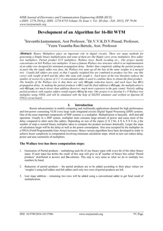
- 2. Development of an Algorithm for 16-Bit WTM DOI: 10.9790/2834-10137986 www.iosrjournals.org 80 | Page Wallace tree multiplier reduction stages for 8X8 multiplication [1]
- 3. Development of an Algorithm for 16-Bit WTM DOI: 10.9790/2834-10137986 www.iosrjournals.org 81 | Page Final Result Bits Improvements to the Algorithm: First stage: It is evident that every multiplication in Wallace tree algorithm is done in three logical stages. They are the partial product generation, the reduction stages and the last stage addition using a conventional adder. If we recall the description for Partial product generation, the first step, we are doing it by use of AND gates. If two 8 bit numbers say A and B are to be multiplied, the algorithm starts at the least significant bits (LSBs) of A and B. LSB of B say b0 will be AND with all the eight bits of A from a0 to a7. This gives us a single row of partial
- 4. Development of an Algorithm for 16-Bit WTM DOI: 10.9790/2834-10137986 www.iosrjournals.org 82 | Page products. The second row of PPs will be generated when all bits of A will be AND with b1. Similarly, every row will be formed due to AND operations. Rows of partial products of 8 bit multiplication Every partial product of first row has b0. Every second row element has b1. Similarly every partial product of nth row will have the common AND input bn-1. So, we can write mathematically the first row as (a7 a6 a5 a4 a3 a2 a1)*b0. Any nth row can be written as (a7 a6 a5 a4 a3 a2 a1)*bn-1. We know that all the above bits are binary digits i.e. either 0 or 1. Hence two possibilities exist. If b0 = 0: Then the first row (a7 a6 a5 a4 a3 a2 a1)*b0 will be equal to (a7 a6 a5 a4 a3 a2 a1)*0 = (0 0 0 0 0 0 0 0) If b0 =1: Then the first row (a7 a6 a5 a4 a3 a2 a1)*b0 will be equal to (a7 a6 a5 a4 a3 a2 a1)*1 = (a7 a6 a5 a4 a3 a2 a1) = A Hence any row will be equal to the Multiplicand A or it will be a row full of Zeros. Keeping the above fact in mind we can use another way to generate partial products for our need without using n2 number of AND gates (n is the size of inputs). This method is given below. Any nth row will be 0 or A based on the value of common input bn-1 of that row. Row „n‟ = 0, if bn-1=0 Row „n‟ =A, if bn-1=1 Consider the following example to comprehend this new logic in a better way. Let A= 11111111 and B=10011011. A is multiplicand and B is multiplier as usual. The rows of partial products for the multiplication A X B are: Row 1 = b0 AND (11111111) = 1 AND (11111111) =11111111 =A Row 2 = b1 AND (11111111) = 0 AND (11111111) =11111111 =A Row 3 = b2 AND (11111111) = 0 AND (11111111) =00000000 =O Row 4 = b3 AND (11111111) = 1 AND (11111111) =11111111 =A Row 5 = b4 AND (11111111) = 1 AND (11111111) =11111111 =A Row 6 = b5 AND (11111111) = 0 AND (11111111) =00000000 =O Row 7 = b6 AND (11111111) = 0 AND (11111111) =00000000 =O Row 8 = b7 AND (11111111) = 1 AND (11111111) =11111111 =A (Or) Simply we can write: Row 1 = A since b0= 1 Row 2 = O since b1= 0 Row 3 = O since b2= 0 Row 4 = A since b3= 1 Row 5 = A since b4= 1
- 5. Development of an Algorithm for 16-Bit WTM DOI: 10.9790/2834-10137986 www.iosrjournals.org 83 | Page Row 6 = O since b5= 0 Row 7 = O since b6= 0 Row 8 = A since b7= 1 Advantage: In case of previous method for a n-bit multiplier, the first stage will require a total of n2 number of AND gates. But with the new method the task of partial product generation will be done by just n number of steps instead of n2 steps. It is important to note that while describing the multiplier in VHDL code, each of the n2 AND operations have to be written manually. For a 32 bit- multiplier it requires 1024 steps to be written for simple AND operations. Instead, with the new modification, only 32 steps are to be written which will save a lot of energy and time to the design engineer during development of the code. So, we have adopted the latter method in designing the WTM system. Representation of signals: As described in an algorithm, we have to use different variables to indicate the partial products in different levels of reduction stages. For example, we used a, b in first stage, then P0, P1 in the next and later S, C, M, N etc. in the figures of chapter 2. These variables are of our choice and we must make sure that PPs in different levels of reduction do not have the same representation. It means that designer has to make a note of which variables he is using in what stage of reduction, clearly and without confusion. There is another sound drawback of representing variables (or „signals‟ with respect to VHDL coding) using normal alphabets like A, B, M or N etc. Let us assume that we have come across a signal N2 while verifying the design. We cannot readily identify which reduction stage this signal N2 belongs to. We must go through the code once again form start and locate where N2 has its origin. Imagine a 32 bit multiplier which will have a very large number of such signals. To go through the code every other time to know about a signal, it is a tremendous burden for the designer. So, it is of high importance that we have a proper representation scheme for signals or variables. We must be able to identify from the name of a signal or variable several aspects. They are: 1. The reduction stage to which it belongs 2. The column or the weight of the partial product 3. Whether it is a SUM bit or CARRY bit 4. If more than one sum and carry bits are present in the column, then position of that bit in the column. Scheme of representation of signals To satisfy the above four requirements, we adopt the above representation scheme.
- 6. Development of an Algorithm for 16-Bit WTM DOI: 10.9790/2834-10137986 www.iosrjournals.org 84 | Page Ri reduction stage number „i‟ ; Eg: R1, R2, R4 etc. Sj sum bit of column „j+1‟ Cj carry bit of column „j+1‟Weight of partial product = 2j k place of the signal in the column. If there are 4 sum bits in the column k takes the values of 1, 2, 3 and 4. Always the sum bits are taken first and the carry bits are taken next to sums. Reverse will also give the same answer, but to avoid confusion sums are given first priority in any column. Let us consider a column having 4 sums and 3 carries. Let all the bits belong to column number 6 (j=5) of 3rd reduction stage. It will be represented as follows. R3S5_1 R3S5_2 R3S5_3 R3S5_4 R3C5_1 R3C5_2 R3C5_3 A column of signals of 3rd reduction stage, 5th column Designing, Synthesis and Results of WTM for the Spartan 3E family FPGA chip Simulated output of WTM Maximum Combinational Path Delay S. No Size of multiplier Maximum combinational path delay (Nano seconds) 1 4 10.426 2 6 11.921 3 8 13.924 4. 10 14.775 5. 12 14.798 6. 14 16.168 7. 16 16.476
- 7. Development of an Algorithm for 16-Bit WTM DOI: 10.9790/2834-10137986 www.iosrjournals.org 85 | Page Comparison of Multipliers w.r.t Delay (ns) Comparison of Multipliers in terms of Area Comparison of Multipliers in terms of PDP Comparison of Multipliers in terms of ADP Size of the multiplier Vs No. of reduction stages 13.924 18.641 26.642 0 20 40 Delay(ns) 8*8 Multiplier WTM CSHM Booth Multiplier 146 169 180 0 100 200 Area(LUT) 8*8 Multiplier WTM CSHM Booth Multiplier 0.724 0.969 1.385 0 1 2 PDP 8*8 Multiplier WTM CSHM Booth Multiplier 8*8 Multiplier WTM 0.271 0.271 0.2353 0.47950 1 ADP 8*8 Multiplier WTM CSHM Booth Multiplier S. No Size of multiplier No. of Reduction Stages Including last stage 1 4 3 4 2 8 4 5 3 16 6 7
- 8. Development of an Algorithm for 16-Bit WTM DOI: 10.9790/2834-10137986 www.iosrjournals.org 86 | Page Features of WTM Conclusion and Discussion It can be concluded that Wallace tree multiplier is superior in all respects like Delay, Area and speed. However array multiplier requires more power consumption and gives optimum number of components required, but it can provides a better delay .If we utilize this multiplier as a module of real time applications like FIR Filter ,it can pump up the Filtering action. Further the work can be extended for optimization of said multiplier to improve speed or to minimize the Power Consumption. References [1]. C. S. Wallace, A Suggestion for a Fast Multiplier, IEEE Transactions on Electronic Computers, February 1964, EC-13:14–17. [2]. Vijaya Prakash A. M, Dr. MGR, K. S. Gurumurthy, A Novel VLSI Architecture for Low power FIR Filter, International Journal of Advanced Engineering & Application, January 2011, PP 218 - 224. [3]. Gary W. Bewick, Fast multiplication algorithms and implementation, The Department Of Electrical Engineering and The Committee on Graduate studies of STANFORD UNIVERSITY, February 1994. PP 8 - 16. [4]. J. Bhasker, AVHDL Primer, Third Edition, Pearson Education, 2007, PP-21 to 50, 88 to 101 [5]. John F. Wakerly, Digital Design Principle and Practices, fourth edition, Prentice Hall Pearson Education, 2009, PP 235-250, PP 786-795 [6]. http://en.wikipedia.org/wiki/Wallace_tree, http://en.wikipedia.org/wiki/FPGA. [7]. Multiplication in FPGA‟s “The performance FPGA DESIGN specialist” Parameter Used Available Pre Layout Values (or) Ratio Number Of Slices 96 371 2448 15% Number of 4-input LUTs 178 647 4896 13% Number Of Bonded Input 32 64 158 40% Number Of Bonded Output 32 64 158 40% Delay(ns) 16.476 Slice Utilization Ratio 100 BRAM Utilization Ratio 100