![Implementation and Simulation Of Ieee…
www.ijesi.org 12 | Page
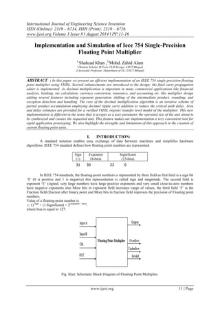
Fig. II(b): Implementation of Floating Point Multiplier.
II. FLOATING POINT MULTIPLICATION ALGORITHM:
Multiplying two numbers in floating point format is done by 1- adding the exponent of the two numbers then subtracting the bias from their result, 2- multiplying the significand of the two numbers, and 3- calculating the sign by XORing the sign of the two numbers. In order to represent the multiplication result as a normalized number there should be 1 in the MSB of the result (leading one). As stated in the floating point format, normalized floating point numbers have the form of as Value = (-1S) * 2 (E - Bias) * (1.M). Fig. III(a): FP Multiplier Operational Flow Chart To multiply two floating point numbers the following is done:
[1] Multiply the significand (1.M1*1.M2 ).
[2] Placing the decimal point in the result
[3] Add the exponents; i.e. (E1+E2– Bias).
[4] Obtaining the sign; i.e. S1 xor S2.
[5] Normalizing the result; i.e. obtaining 1 at the MSB of the results‟ significand.
[6] Rounding the result to fit in the available bits.
[7] Checking for underflow/overflow occurrence.
Consider a floating point representation similar to the IEEE 754 single precision floating point format, but with a reduced](data:image/gif;base64,R0lGODlhAQABAIAAAAAAAP///yH5BAEAAAAALAAAAAABAAEAAAIBRAA7)
Recommended
More Related Content
What's hot
What's hot (20)
Similar to Implementation and Simulation of Ieee 754 Single-Precision Floating Point Multiplier
Similar to Implementation and Simulation of Ieee 754 Single-Precision Floating Point Multiplier (20)
Recently uploaded
Recently uploaded (20)
Implementation and Simulation of Ieee 754 Single-Precision Floating Point Multiplier
- 1. International Journal of Engineering Science Invention ISSN (Online): 2319 – 6734, ISSN (Print): 2319 – 6726 www.ijesi.org Volume 3 Issue 8 ǁ August 2014 ǁ PP.11-16 www.ijesi.org 11 | Page Implementation and Simulation of Ieee 754 Single-Precision Floating Point Multiplier 1,Shahzad Khan ,2,Mohd. Zahid Alam 1,(Student Scholar M.Tech, VLSI Design, LNCT Bhopal) 2(Associate Professor, Department of EC, LNCT Bhopal) ABSTRACT : In this paper we present an efficient implementation of an IEEE 754 single precision floating point multiplier using VHDL. Several enhancements are introduced to the design; the final carry propagation adder is implemented. As decimal multiplication is important in many commercial applications like financial analysis, banking, tax calculation, currency conversion, insurance, and accounting etc. this multiplier design adding several features including exponent generation, shifting of the intermediate product, rounding, and exception detection and handling. The core of the decimal multiplication algorithm is an iterative scheme of partial product accumulation employing decimal ripple carry addition to reduce the critical path delay. Area and delay estimates are provided for a verified VHDL register transfer level model of the multiplier. This new implementation is different in the sense that it accepts as a user parameter the operated size of the unit about to be synthesized and creates the requested unit. This feature makes our implementation a very convenient tool for rapid application prototyping. We also highlight the strengths and limitations of this approach in the creation of custom floating point units. I. INTRODUCTION: A standard notation enables easy exchange of data between machines and simplifies hardware algorithms. IEEE 754 standard defines how floating point numbers are represented. In IEEE 754 standards, the floating-point numbers is represented by three field as first field is a sign bit „S‟ (0 is positive and 1 is negative) this representation is called sign and magnitude. The second field is exponent „E‟ (signed, very large numbers have large positive exponents and very small close-to-zero numbers have negative exponents also More bits in exponent field increases range of values, the third field „F‟ is the Fraction field (fraction after binary point and More bits in fraction field improves the precision of Floating point numbers. Value of a floating-point number is (–1) Sign × (1.Significant) × 2(exponent – bias). where bias is equal to 127. Fig. II(a): Schematic Block Diagram of Floating Point Multiplier. Sign (1) Exponent (8-bits) Significant (23-bits) 31 30 22 0
- 2. Implementation and Simulation Of Ieee… www.ijesi.org 12 | Page Fig. II(b): Implementation of Floating Point Multiplier. II. FLOATING POINT MULTIPLICATION ALGORITHM: Multiplying two numbers in floating point format is done by 1- adding the exponent of the two numbers then subtracting the bias from their result, 2- multiplying the significand of the two numbers, and 3- calculating the sign by XORing the sign of the two numbers. In order to represent the multiplication result as a normalized number there should be 1 in the MSB of the result (leading one). As stated in the floating point format, normalized floating point numbers have the form of as Value = (-1S) * 2 (E - Bias) * (1.M). Fig. III(a): FP Multiplier Operational Flow Chart To multiply two floating point numbers the following is done: [1] Multiply the significand (1.M1*1.M2 ). [2] Placing the decimal point in the result [3] Add the exponents; i.e. (E1+E2– Bias). [4] Obtaining the sign; i.e. S1 xor S2. [5] Normalizing the result; i.e. obtaining 1 at the MSB of the results‟ significand. [6] Rounding the result to fit in the available bits. [7] Checking for underflow/overflow occurrence. Consider a floating point representation similar to the IEEE 754 single precision floating point format, but with a reduced
- 3. Implementation and Simulation Of Ieee… www.ijesi.org 13 | Page number of mantissa bits (only 4) while still retaining the hidden „1‟ bit for normalized numbers: A = 0 10000100 0100 = 40, B = 1 10000001 1110 = -7.5 To multiply A and B 1. Multiply significand: 1.0100×1.1110 00000 10100 10100 10100 10100 1001011000 2. Place the decimal point: 10.01011000 3. Add exponents: 10000100+10000001= 100000101 The exponent representing the two numbers is already shifted/biased by the bias value (127) and is not the true exponent; i.e. EA = EA-true + bias and EB = EB-true + bias And EA + EB = EA-true + EB-true + 2 bias So we should subtract the bias from the resultant exponent otherwise the bias will be added twice. 100000101 - 01111111 10000110 4. Obtain the sign bit and put the result together: 10000110 10.01011000 5. Normalize the result so that there is a 1 just before the radix point (decimal point). Moving the radix point one place to the left increments the exponent by 1; moving one place to the right decrements the exponent by 1. 1 10000110 10.01011000 (before normalizing) 1 10000111 1.001011000 (normalized) The result is (without the hidden bit): 1 10000111 00101100 6. The mantissa bits are more than 4 bits (mantissa available bits); rounding is needed. If we applied the truncation rounding mode then the stored value is: 1 10000111 0010. Fig. III(b) shows the multiplier structure; Exponents addition, Significand multiplication, and Result‟s sign calculation are independent and are done in parallel. The significand multiplication is done on two 24 bit numbers and results in a 48 bit product, which we will call the intermediate product (IP). The IP is represented as (47 down to 0) and the decimal point is located between bits 46 and 45 in the IP. The following sections detail each block of the floating point multiplier. Fig. III(b): Floating Point Multiplier Block Diagram
- 4. Implementation and Simulation Of Ieee… www.ijesi.org 14 | Page III. HARDWARE OF FLOATING POINT MULTIPLIER A. Sign bit calculation Multiplying two numbers results in a negative sign number if one of the multiplied numbers is of a negative value. By the aid of a truth table we find that this can be obtained by XORing the sign of two inputs. B. Unsigned Adder (for exponent addition) : It is possible to create a logical circuit using multiple full adders to add N-bit numbers. Each full adder inputs a Cin, which is the Cout of the previous adder. This kind of adder is called a ripple-carry adder, since each carry bit "ripples" to the next full adder. Note that the first (and only the first) full adder may be replaced by a half adder. The layout of a ripple-carry adder is simple, which allows for fast design time; however, the ripple-carry adder is relatively slow, since each full adder must wait for the carry bit to be calculated from the previous full adder. The gate delay can easily be calculated by inspection of the full adder circuit. Each full adder requires three levels of logic. In a 32-bit ripple-carry adder, there are 32 full adders, so the critical path (worst case) delay is 3 (from input to carry in first adder) + 31 * 2 (for carry propagation in later adders) = 65 gate delays. A design with alternating carry polarities and optimized AND-OR-Invert gates can be about twice as fast. Multiple full adder circuits can be cascaded in parallel to add an N-bit number. For an N- bit parallel adder, there must be N number of full adder circuits. A ripple carry adder is a logic circuit in which the carry-out of each full adder is the carry in of the succeeding next most significant full adder. It is called a ripple carry adder because each carry bit gets rippled into the next stage. In a ripple carry adder the sum and carry out bits of any half adder stage is not valid until the carry in of that stage occurs. Propagation delays inside the logic circuitry are the reason behind this. Propagation delay is time elapsed between the application of an input and occurrence of the corresponding output. Consider a NOT gate, When the input is “0″ the output will be “1″ and vice versa. The time taken for the NOT gate‟s output to become “0″ after the application of logic “1″ to the NOT gate‟s input is the propagation delay here. Similarly the carry propagation delay is the time elapsed between the application of the carry in signal and the occurrence of the carry out (Cout) signal. Fig. IV (a) Ripple Carry Adder. C. Multiplier for Unsigned Data : Multiplication involves the generation of partial products, one for each digit in the multiplier, as in Fig8. These partial products are then summed to produce the final product. The multiplication of two n-bit binary integers results in a product of up to 2n bits in length. Fig. IV (b): A Schematic of multiplier. D. Normalizer : The result of the significand multiplication (intermediate product) must be normalized to have a leading „1‟ just to the left of the decimal point (i.e. in the bit 46 in the intermediate product). Since the inputs are normalized numbers then the intermediate product has the leading one at bit 46 or 47.
- 5. Implementation and Simulation Of Ieee… www.ijesi.org 15 | Page 1- If the leading one is at bit 46 (i.e. to the left of the decimal point) then the intermediate product is already a normalized number and no shift is needed. 2- If the leading one is at bit 47 then the intermediate product is shifted to the right and the exponent is incremented by 1. The shift operation is done using combinational shift logic made by multiplexers. IV. UNDERFLOW/OVERFLOW DETECTION Overflow/underflow means that the result‟s exponent is too large/small to be represented in the exponent field. The exponent of the result must be 8 bits in size, and must be between 1 and 254 otherwise the value is not a normalized one. An overflow may occur while adding the two exponents or during normalization. Overflow due to exponent addition may be compensated during subtraction of the bias; resulting in a normal output value (normal operation). An underflow may occur while subtracting the bias to form the intermediate exponent. If the intermediate exponent < 0 then it‟s an underflow that can never be compensated; if the intermediate exponent = 0 then it‟s an underflow that may be compensated during normalization by adding 1 to it. When an overflow occurs an overflow flag signal goes high and the result turns to ±Infinity (sign determined according to the sign of the floating point multiplier inputs). When an underflow occurs an underflow flag signal goes high and the result turns to ±Zero (sign determined according to the sign of the floating point multiplier inputs). Denormalized numbers are signaled to Zero with the appropriate sign calculated from the inputs and an underflow flag is raised. Assume that E1 and E2 are the exponents of the two numbers A and B respectively; the result‟s exponent is calculated by Eresult = E1 + E2 – 127. E1 and E2 can have the values from 1 to 254; resulting in Eresult having values from -125 (2-127) to 381 (508- 127); but for normalized numbers, Eresult can only have the values from 1 to 254. Table I summarizes the Eresult different values and the effect of normalization on it. Table I: Normalization Effect On Result‟s Exponent And Overflow/Underflow Detection V. SIMULATION RESULTS Fig. V(a): RTL Schematic of FP Multiplier. ERESULT Specification Observation -125 = ERESULT < 0 Underflow Cannot be compensated during normalize ERESULT = 0 Zero May turn to normalized number during normalization 1 < ERESULT < 254 Normalised Number May result in overflow during normalization 255 = ERESULT Overflow Cannot be compensated
- 6. Implementation and Simulation Of Ieee… www.ijesi.org 16 | Page Fig. V(b): Simulation Result of FP Multiplier. CONCLUSION: The new design of multiplier has efficient in operation as well as has used less components as need of Subtractor circuit for the exponent calculation also reduced and the delay time for the multiplication is 14 nanosecond which is also less than the previously designed multipliers. So we say that the proposed multiplier has efficient in operation and cost. This paper presents an implementation of a floating point multiplier that supports the IEEE 754 -2008 binary interchange format; the multiplier doesn‟t implement rounding and just presents the significand multiplication result as is (48 bits); this gives better precision if the whole 48 bits are utilized in another unit. REFERENCES: [1] Pierre, L. “VHDL description and formal verification of systolic multipliers. In CHDL”, N. Holland, 1993. [2] A. Kaldewaij, “Programming: The Derivation of Algorithms”, Prentice-Hall, 1990. [3] John G. Proakis and Dimitris G. Manolakis (1996), “Digital Signal Processing: Principles,. Algorithms and Applications”, Third Edition. [4] A. D. Booth, “A signed binary multiplication technique”. Quart. J. of Mech. Appl. Math, 4(2), 1951. [5] Volnei A. Pedroni: “Circuit Design and Simulation with VHDL”, Second edition, PHI. [6] BROWN, Stephen D., “Fundamentals of Digital Logic with VHDL design”, Boston: McGraw-Hill, 2000. [7] Peter J. Ashenden, “The Designer‟s Guide to VHDL”, Morgan Kaufmann Publishers, 95 Inc., 1996. [8] V. Kantabulra, “Designing optimum one-level carry-skip adders,” IEEE Transactions on Computers, vol. 42, no. 6, pp. 759-764, June 1993. [9] Beebe, H.F.Nelson, “Floating Point Arithmetic, Computation in Modern Science & Technology”, December, 2007. [10] N. Weste, D. Harris, “CMOS VLSI Design”, Third Edition, Addison Wesley, 2004.