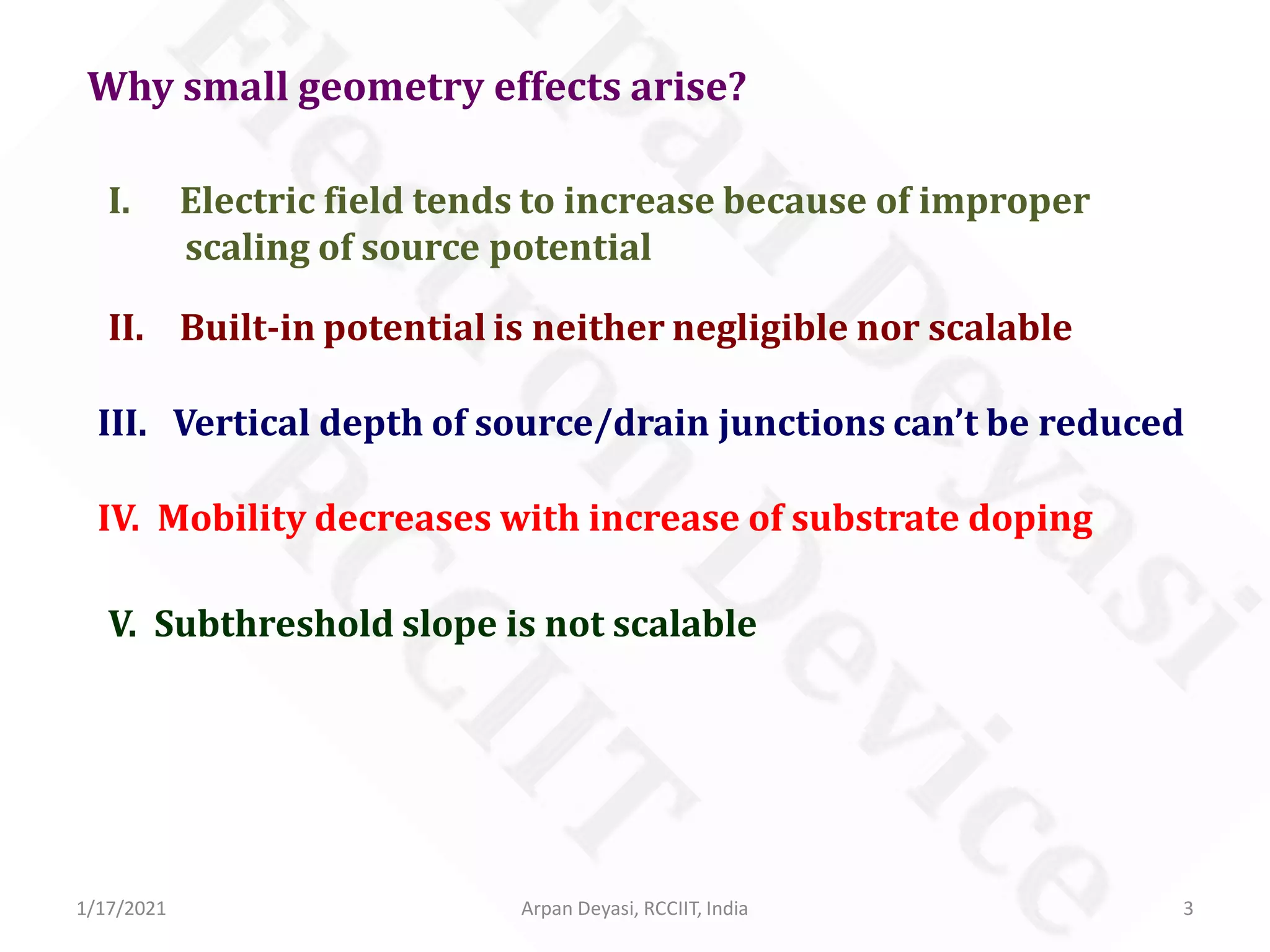
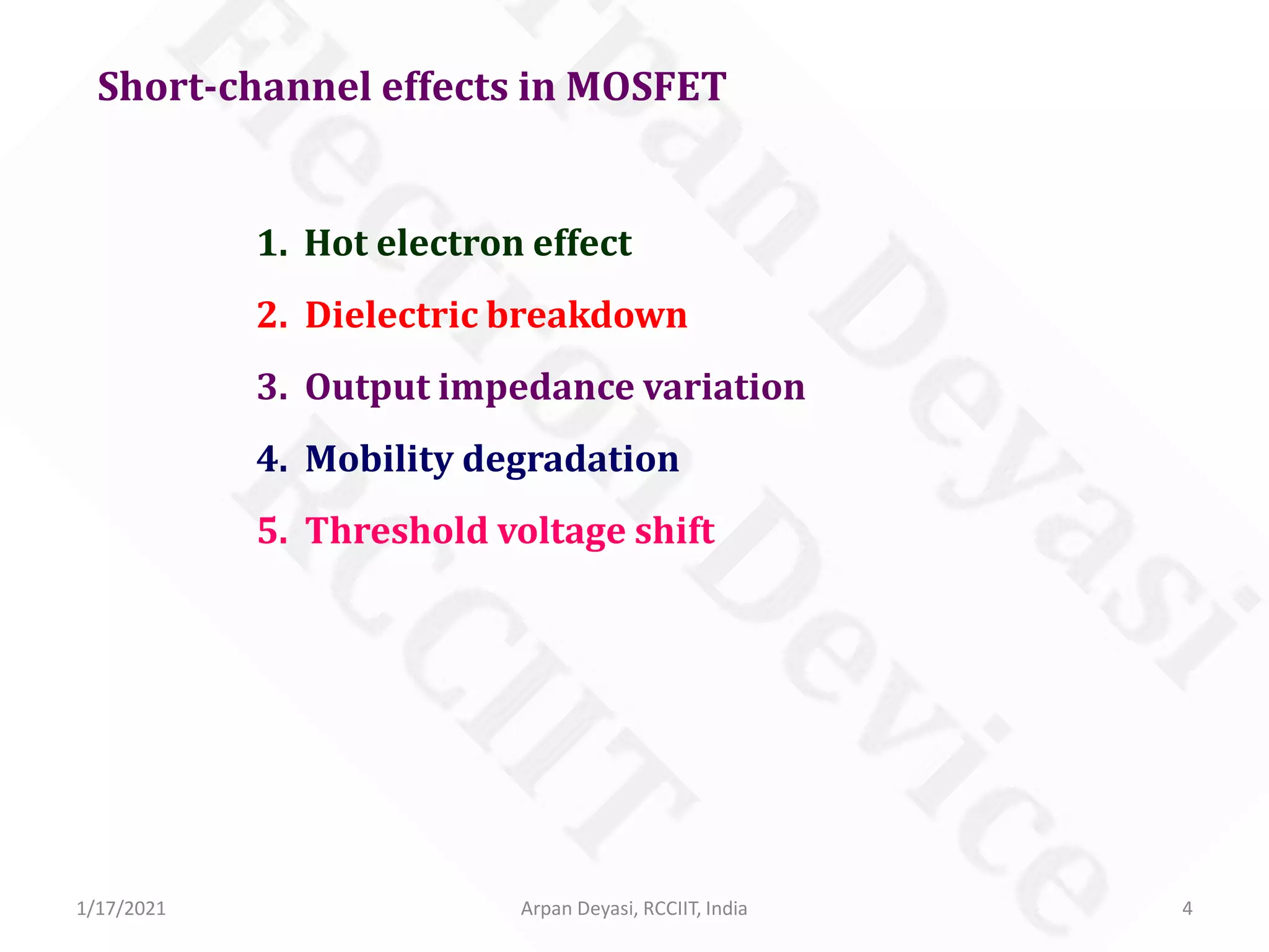
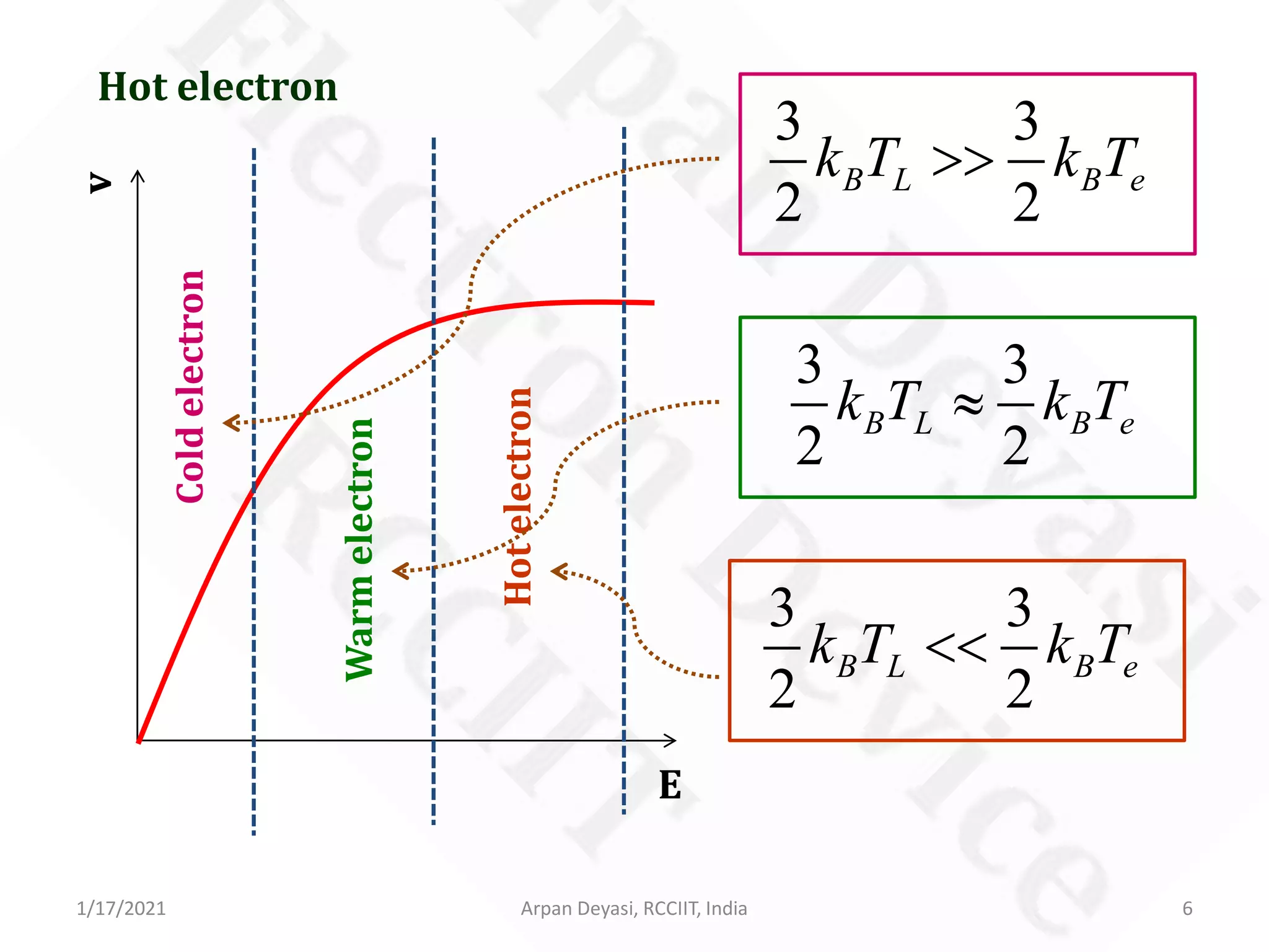
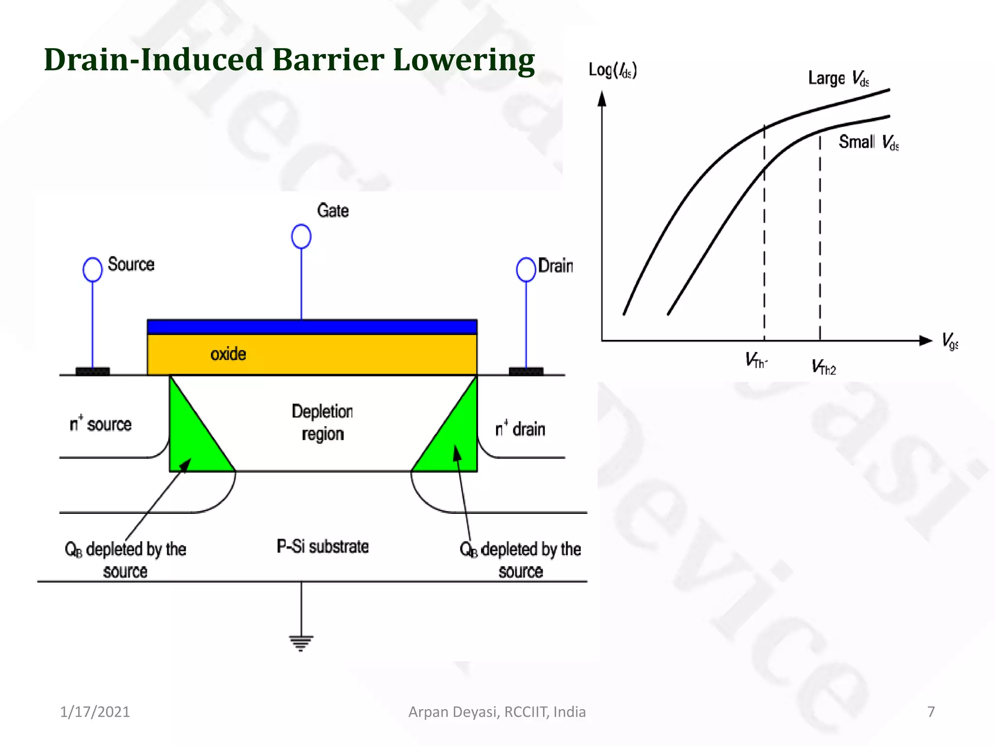
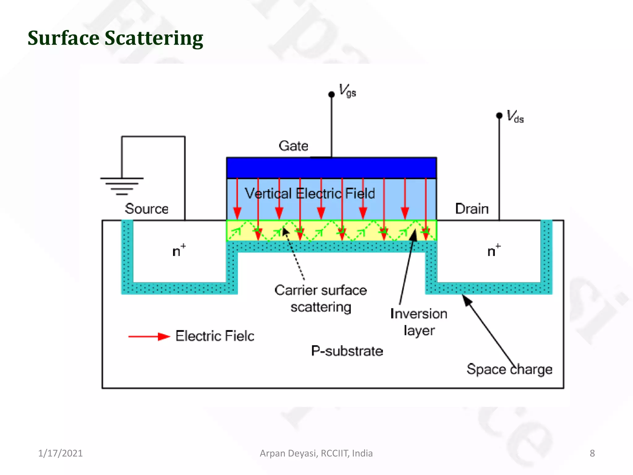
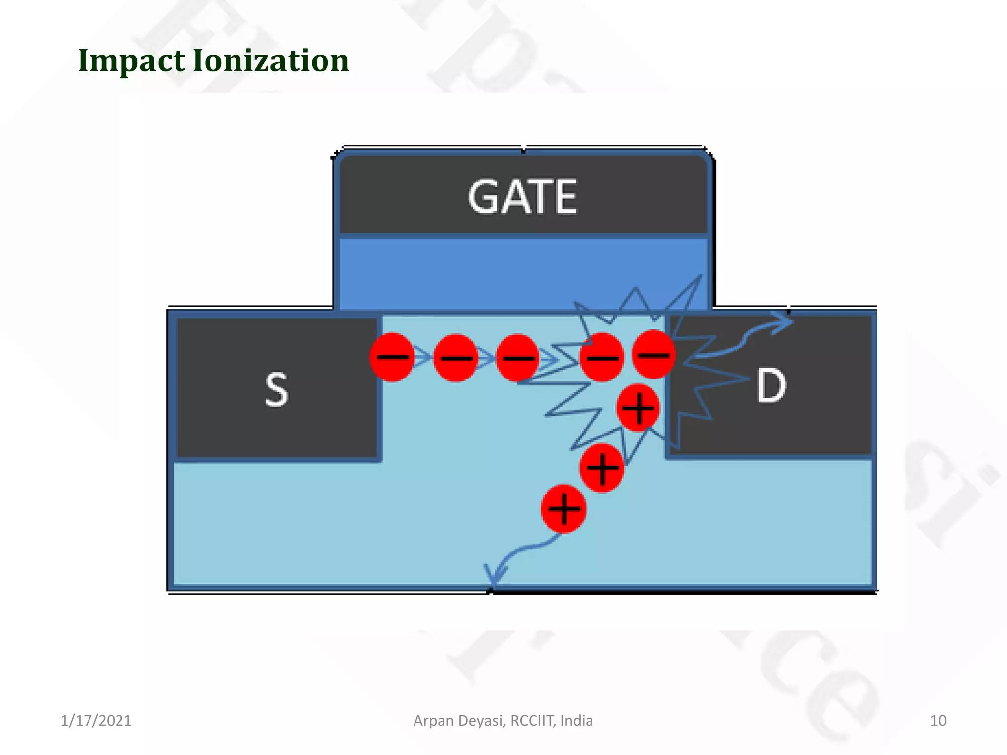
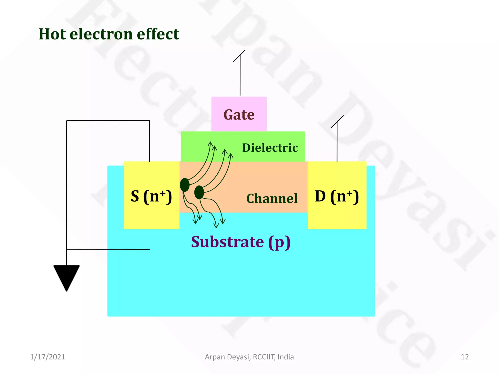
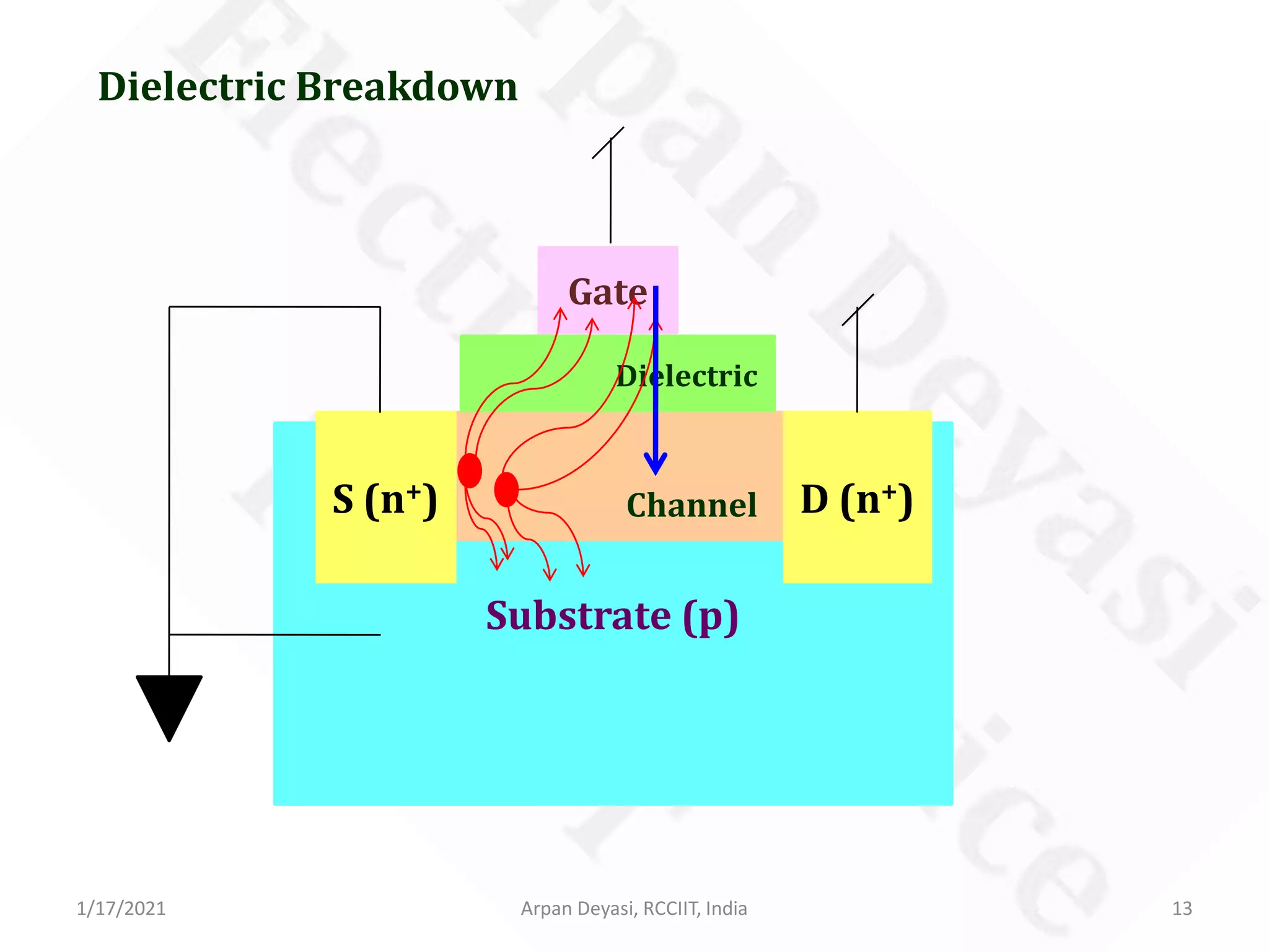
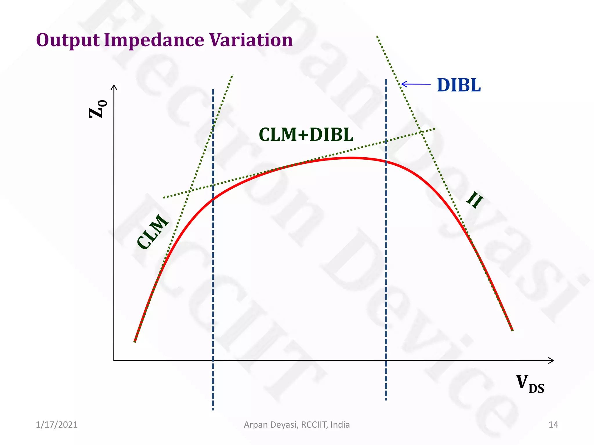
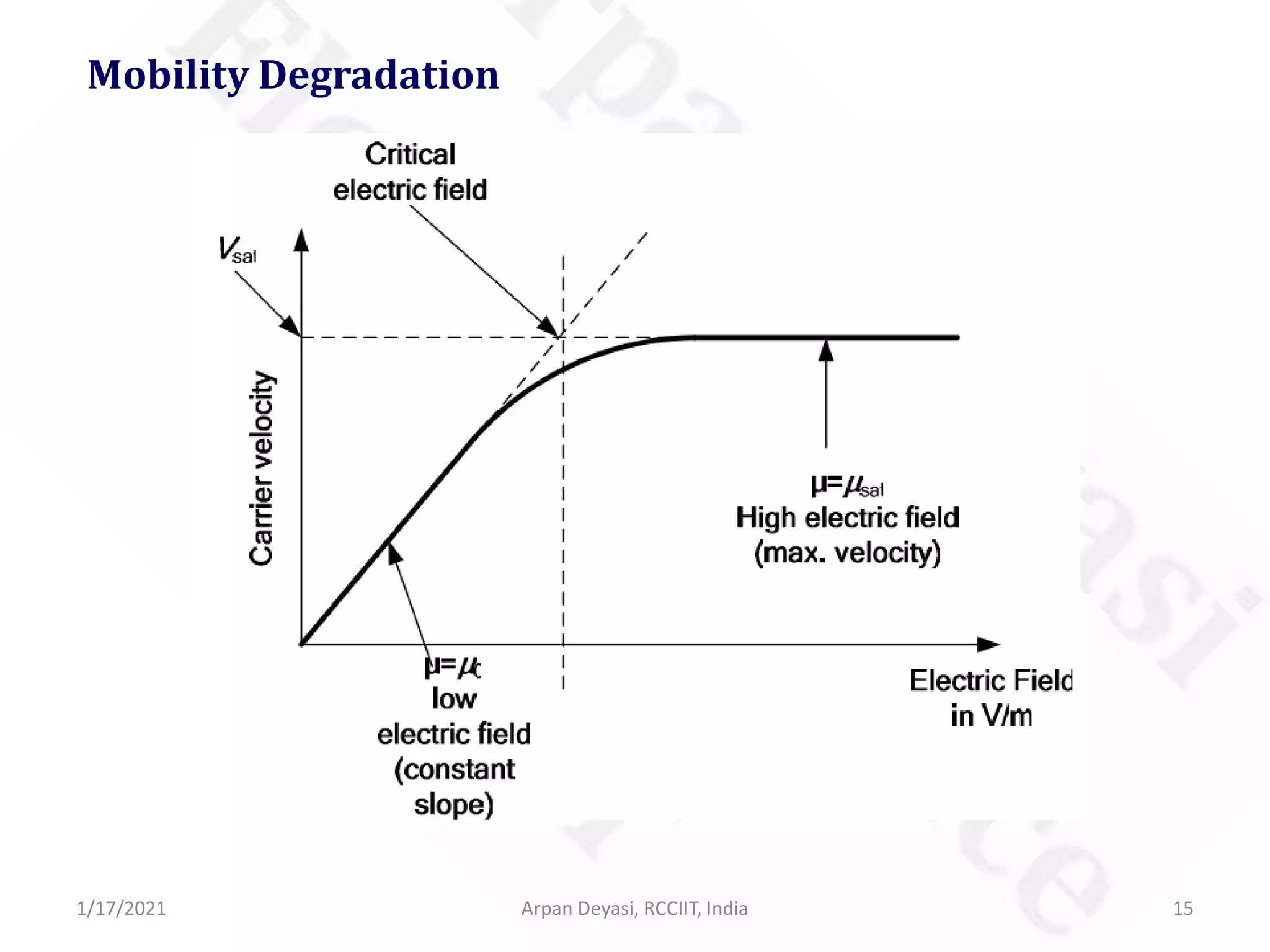
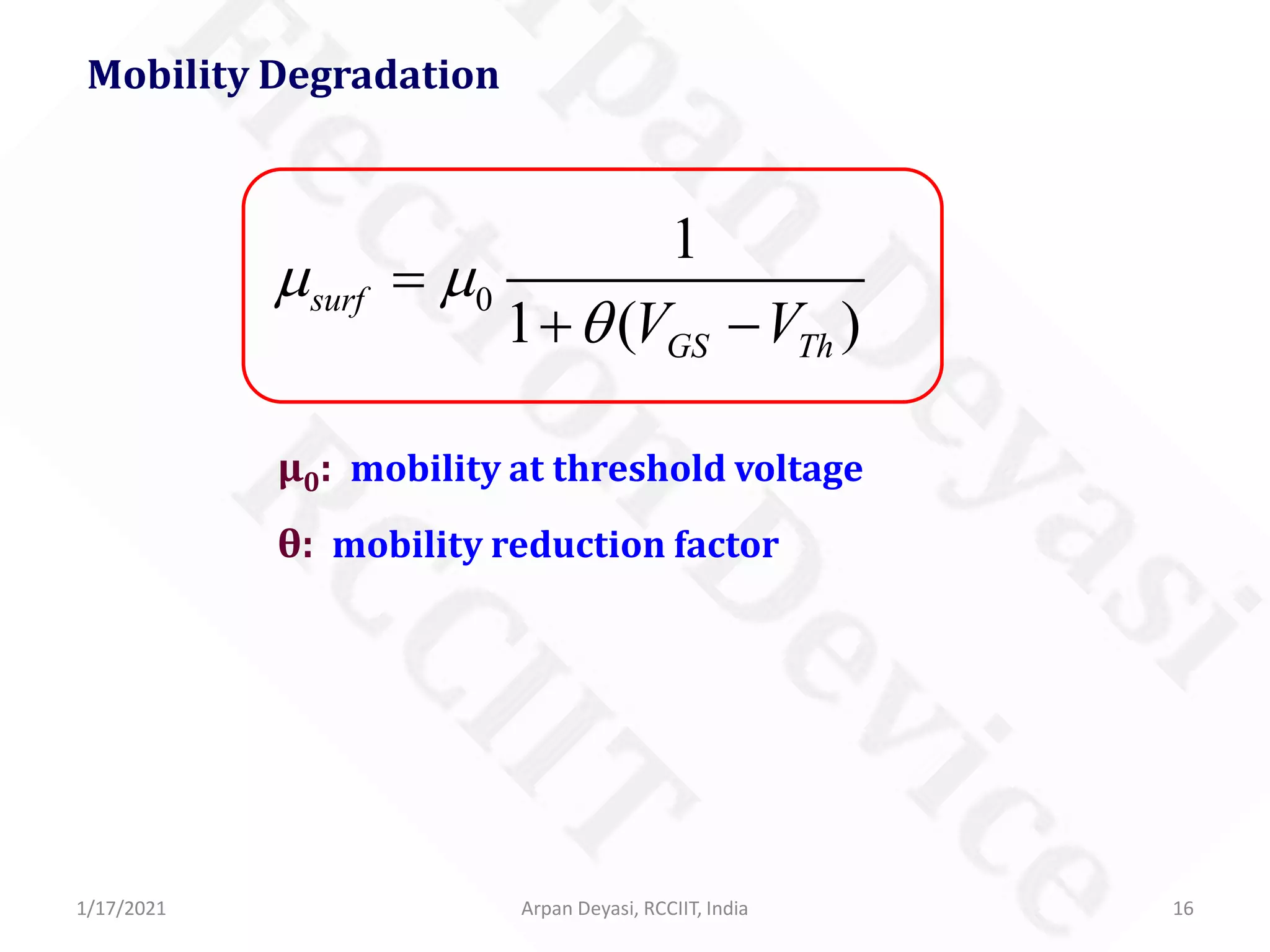
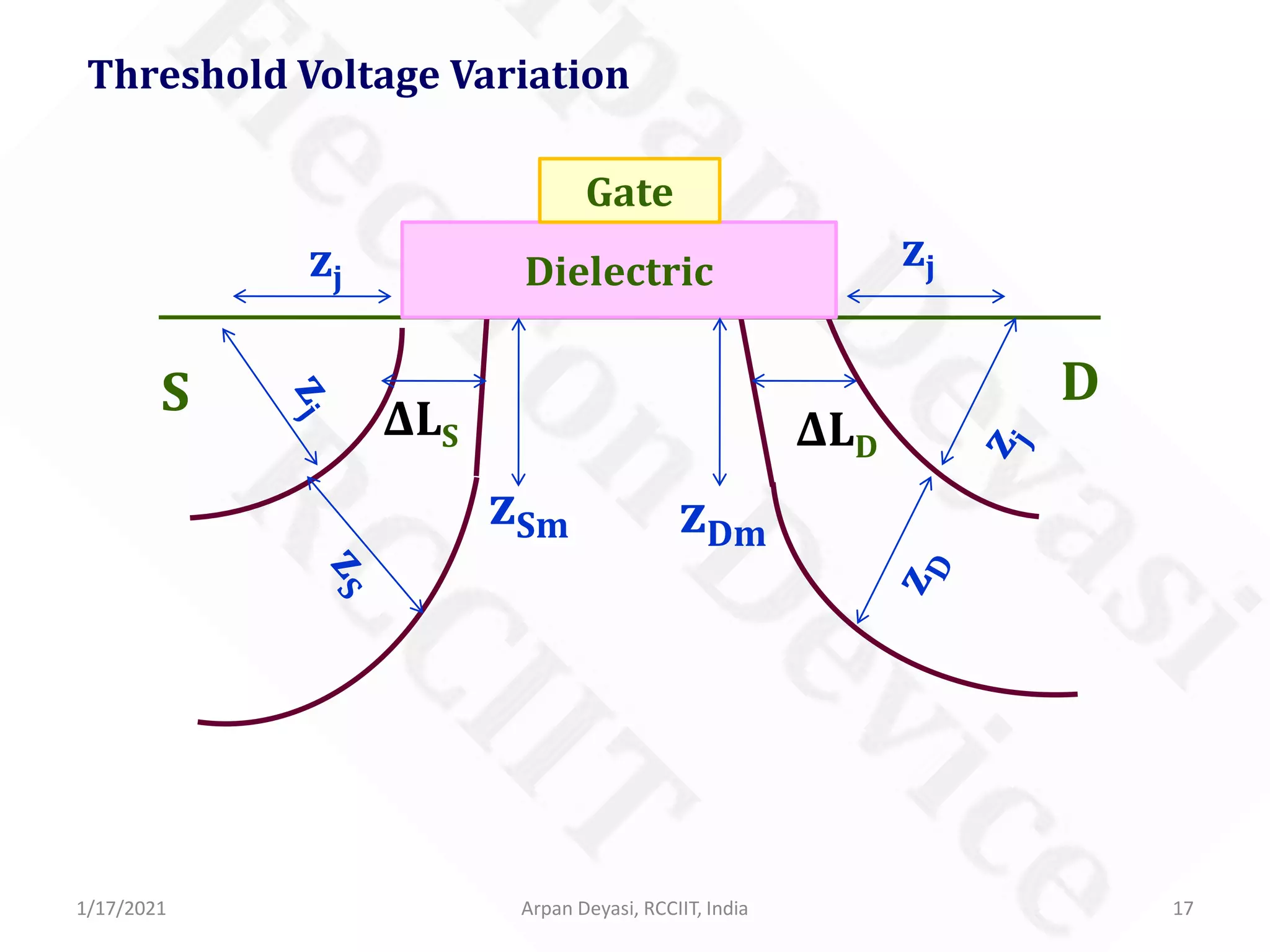
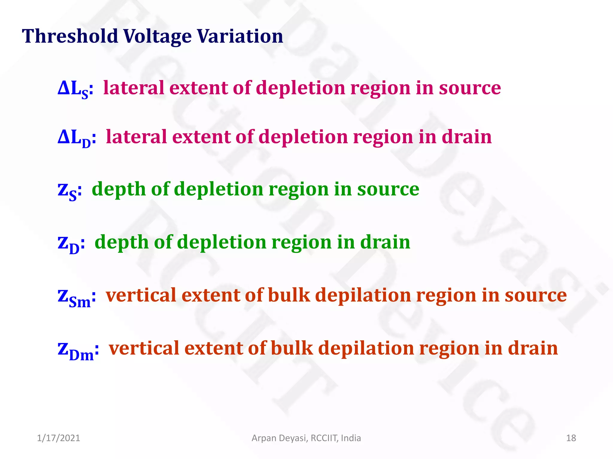
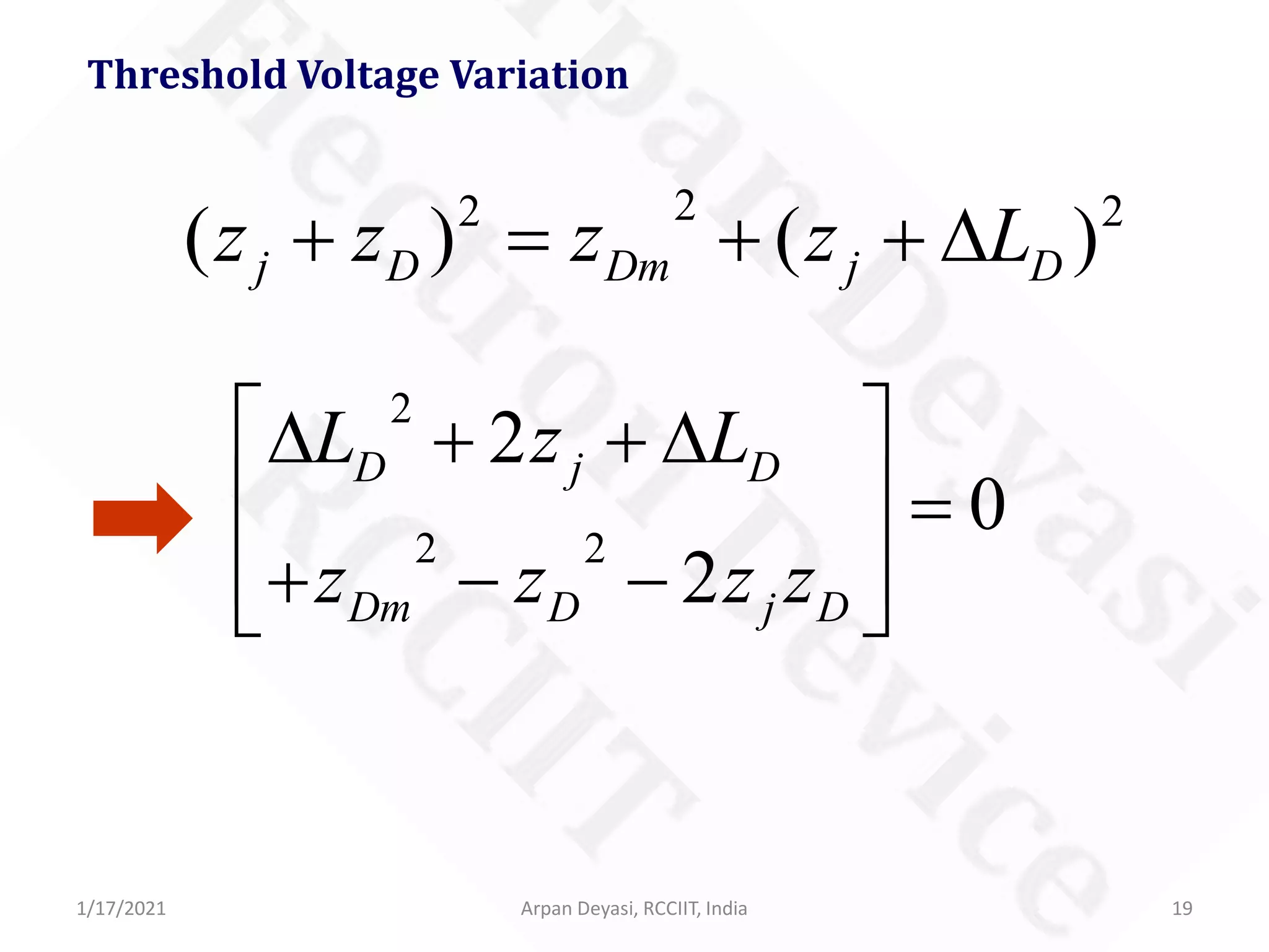
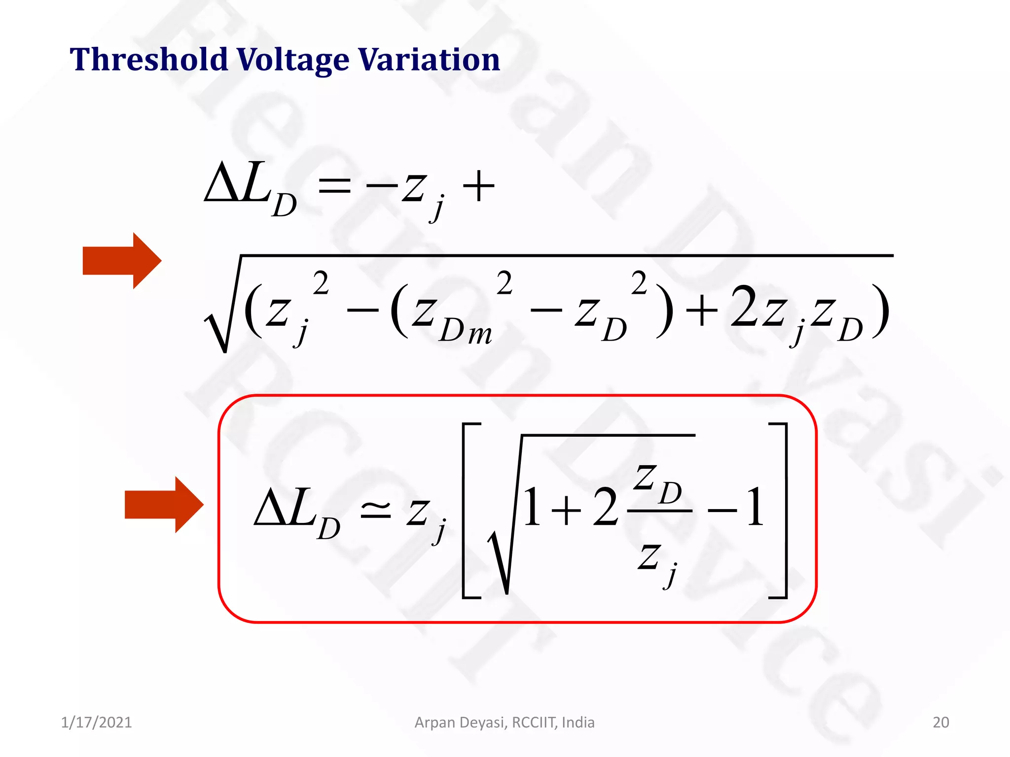
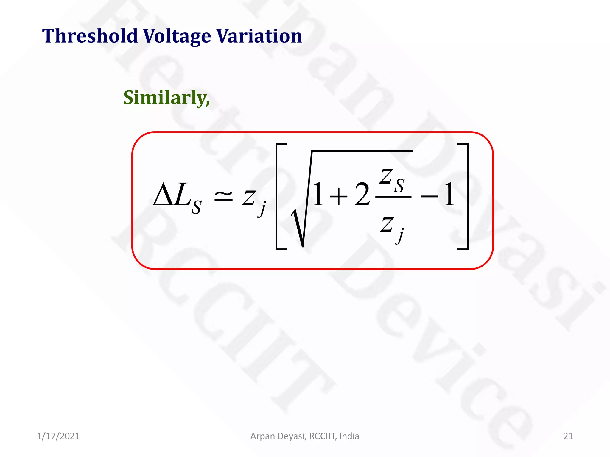
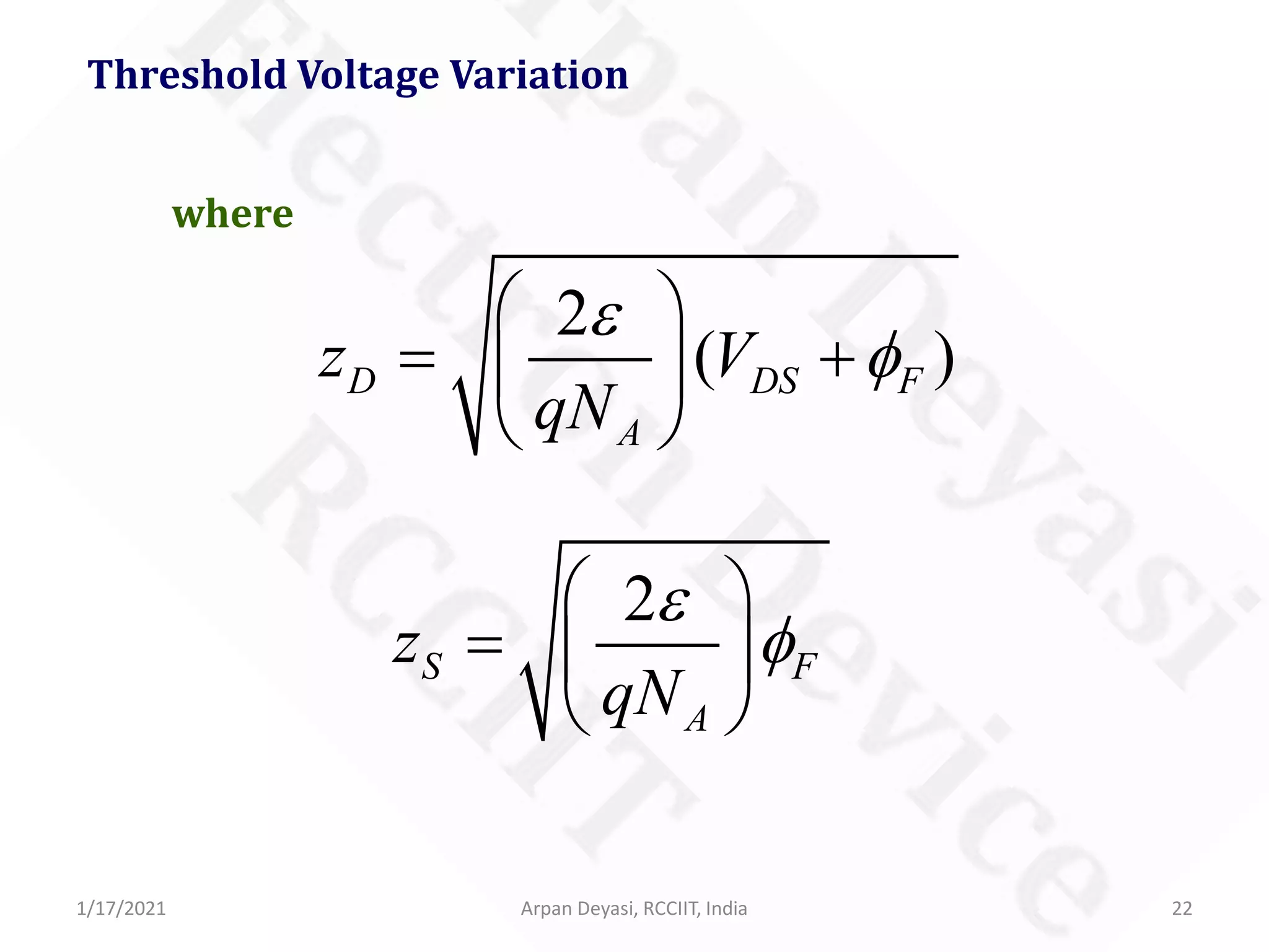
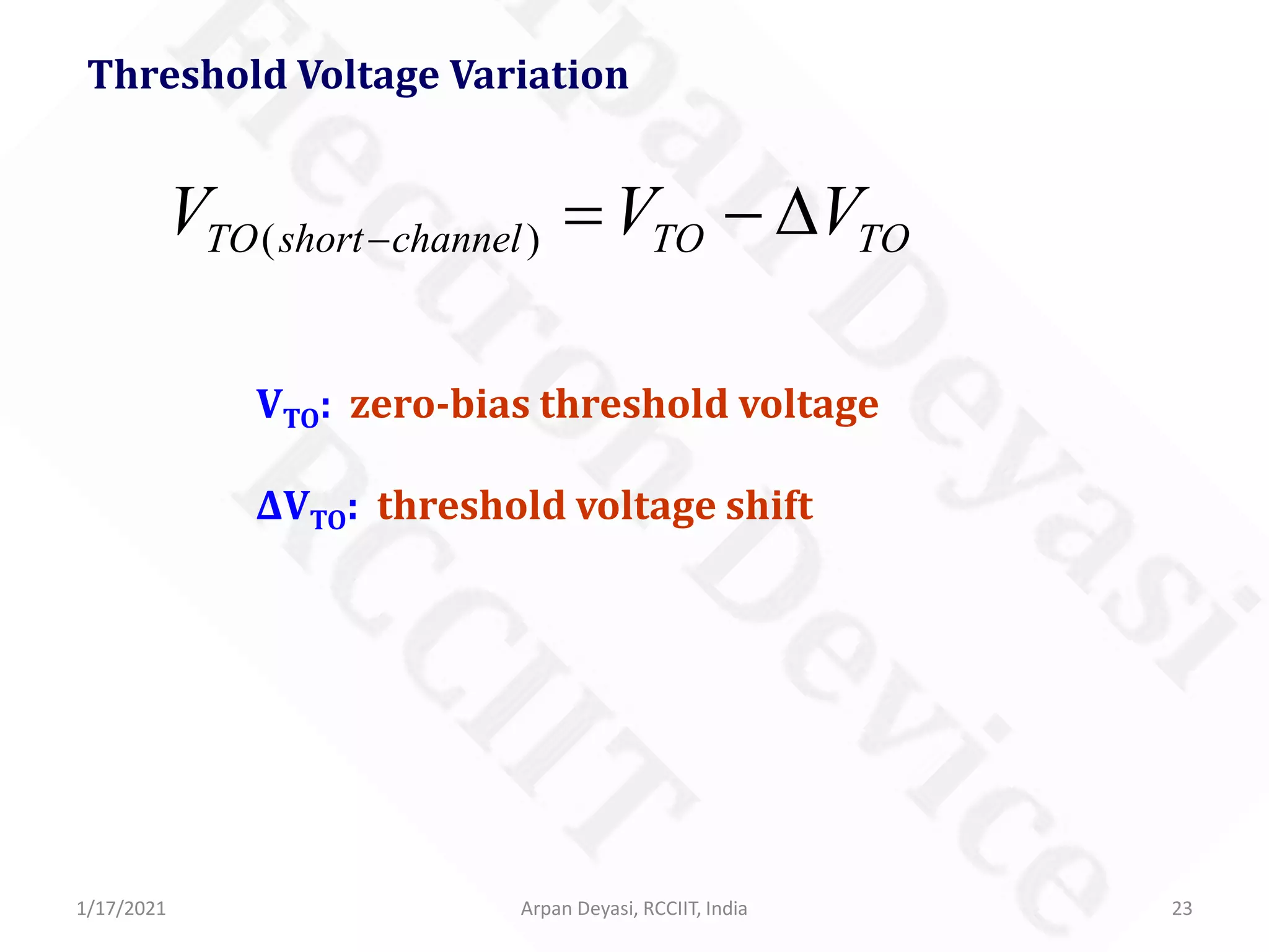
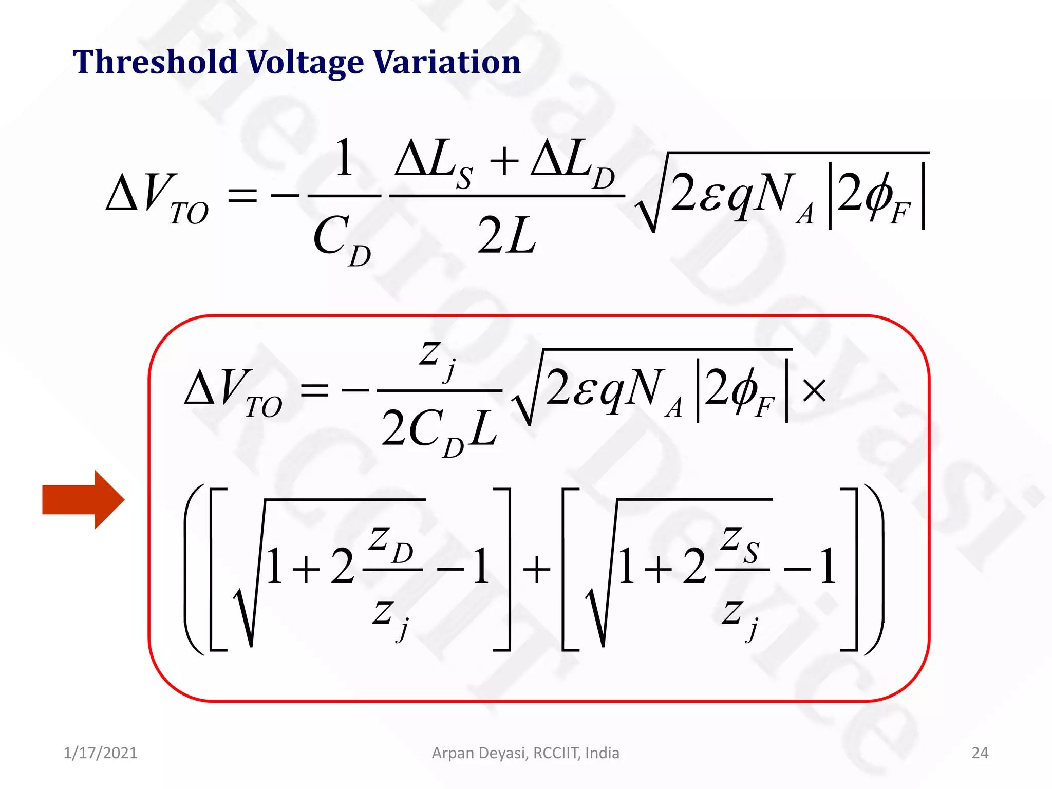
SlideShare a Scribd company logo
1 of 24
Short Channel Effect
in MOSFET
Arpan Deyasi
Dept of ECE, RCCIIT, Kolkata, India
1/17/2021 1Arpan Deyasi, RCCIIT, India
Q. What is meant by short-channel?
Leff≃(zD+zS)
Leff
zDzS
Dielectric
1/17/2021 2Arpan Deyasi, RCCIIT, India
DrainSource
Channel
1/17/2021 3Arpan Deyasi, RCCIIT, India
I. Electric field tends to increase because of improper
scaling of source potential
II. Built-in potential is neither negligible nor scalable
III. Vertical depth of source/drain junctions can’t be reduced
IV. Mobility decreases with increase of substrate doping
V. Subthreshold slope is not scalable
Why small geometry effects arise?
1/17/2021 4Arpan Deyasi, RCCIIT, India
Short-channel effects in MOSFET
1. Hot electron effect
2. Dielectric breakdown
3. Output impedance variation
4. Mobility degradation
5. Threshold voltage shift
1/17/2021 Arpan Deyasi, RCCIIT, India 5
A few related
physical phenomena
1/17/2021 6Arpan Deyasi, RCCIIT, India
Hot electron
Coldelectron
Warmelectron
Hotelectron
3 3
2 2
B L B ek T k T>>
3 3
2 2
B L B ek T k T≈
3 3
2 2
B L B ek T k T<<
E
v
1/17/2021 Arpan Deyasi, RCCIIT, India 7
Drain-Induced Barrier Lowering
1/17/2021 Arpan Deyasi, RCCIIT, India 8
Surface Scattering
1/17/2021 Arpan Deyasi, RCCIIT, India 9
Channel Length Modulation
1/17/2021 Arpan Deyasi, RCCIIT, India 10
Impact Ionization
1/17/2021 Arpan Deyasi, RCCIIT, India 11
Effects of
Short-Channel Geometry
1/17/2021 12Arpan Deyasi, RCCIIT, India
Hot electron effect
Substrate (p)
S (n+) D (n+)
Gate
Channel
Dielectric
1/17/2021 13Arpan Deyasi, RCCIIT, India
Dielectric Breakdown
Substrate (p)
S (n+) D (n+)
Gate
Channel
Dielectric
1/17/2021 14Arpan Deyasi, RCCIIT, India
Output Impedance Variation
CLM+DIBL
VDS
Z0
DIBL
1/17/2021 15Arpan Deyasi, RCCIIT, India
Mobility Degradation
1/17/2021 16Arpan Deyasi, RCCIIT, India
Mobility Degradation
0
1
1 ( )
surf
GS ThV V
µ µ
θ
=
+ −
μ0: mobility at threshold voltage
θ: mobility reduction factor
1/17/2021 17Arpan Deyasi, RCCIIT, India
Threshold Voltage Variation
Dielectric
S D
Gate
zSm zDm
ΔLS ΔLD
zj
zj
1/17/2021 18Arpan Deyasi, RCCIIT, India
ΔLS: lateral extent of depletion region in source
ΔLD: lateral extent of depletion region in drain
zS: depth of depletion region in source
zD: depth of depletion region in drain
zSm: vertical extent of bulk depilation region in source
zDm: vertical extent of bulk depilation region in drain
Threshold Voltage Variation
1/17/2021 Arpan Deyasi, RCCIIT, India 19
22 2
( ) ( )j D Dm j Dz z z z L+ = + + ∆
Threshold Voltage Variation
2
2 2
2
0
2
D j D
Dm D j D
L z L
z z z z
 ∆ + + ∆
  =
 + − − 
1/17/2021 Arpan Deyasi, RCCIIT, India 20
Threshold Voltage Variation
2 2 2
( ( ) 2 )
D j
j D D j Dm
L z
z z z z z
∆ =− +
− − +
1 2 1D
D j
j
z
L z
z
 
∆ + − 
  

1/17/2021 Arpan Deyasi, RCCIIT, India 21
Threshold Voltage Variation
Similarly,
1 2 1S
S j
j
z
L z
z
 
∆ + − 
  

1/17/2021 Arpan Deyasi, RCCIIT, India 22
where
Threshold Voltage Variation
2
( )D DS F
A
z V
qN
ε
φ
 
= + 
 
2
S F
A
z
qN
ε
φ
 
=  
 
1/17/2021 Arpan Deyasi, RCCIIT, India 23
( )TO short channel TO TOV V V− = − ∆
Threshold Voltage Variation
VTO: zero-bias threshold voltage
ΔVTO: threshold voltage shift
1/17/2021 Arpan Deyasi, RCCIIT, India 24
Threshold Voltage Variation
1
2 2
2
S D
TO A F
D
L L
V qN
C L
ε φ
∆ + ∆
∆ =−
2 2
2
1 2 1 1 2 1
j
TO A F
D
SD
j j
z
V qN
C L
zz
z z
ε φ∆ =− ×
    
 + − + + −   
        

More Related Content

What's hot

Vlsi design mosfet
Vlsi design mosfetVlsi design mosfet
Vlsi design mosfet
vennila12
 

What's hot (20)

JFET
JFETJFET
JFET
 
Electrical characteristics of MOSFET
Electrical characteristics of MOSFETElectrical characteristics of MOSFET
Electrical characteristics of MOSFET
 
Mosfet fundamentals
Mosfet fundamentalsMosfet fundamentals
Mosfet fundamentals
 
Metal-Semiconductor Contact
Metal-Semiconductor ContactMetal-Semiconductor Contact
Metal-Semiconductor Contact
 
DoS of bulk and quantum structures
DoS of bulk and quantum structuresDoS of bulk and quantum structures
DoS of bulk and quantum structures
 
Esd
EsdEsd
Esd
 
Carrier transport processes
Carrier transport processesCarrier transport processes
Carrier transport processes
 
Introduction to FinFET
Introduction to FinFETIntroduction to FinFET
Introduction to FinFET
 
Short Channel Effect In MOSFET
Short Channel Effect In MOSFETShort Channel Effect In MOSFET
Short Channel Effect In MOSFET
 
Vlsi design mosfet
Vlsi design mosfetVlsi design mosfet
Vlsi design mosfet
 
MOS transistor 13
MOS transistor 13MOS transistor 13
MOS transistor 13
 
Switched capacitor
Switched capacitorSwitched capacitor
Switched capacitor
 
Foundation of MOS Capacitor
Foundation of MOS CapacitorFoundation of MOS Capacitor
Foundation of MOS Capacitor
 
Mosfet
MosfetMosfet
Mosfet
 
SigmaDeltaADC
SigmaDeltaADCSigmaDeltaADC
SigmaDeltaADC
 
Short channel effect on FET
Short channel effect on FETShort channel effect on FET
Short channel effect on FET
 
IC Design of Power Management Circuits (IV)
IC Design of Power Management Circuits (IV)IC Design of Power Management Circuits (IV)
IC Design of Power Management Circuits (IV)
 
Threshold Voltage & Channel Length Modulation
Threshold Voltage & Channel Length ModulationThreshold Voltage & Channel Length Modulation
Threshold Voltage & Channel Length Modulation
 
Device isolation Techniques
Device isolation TechniquesDevice isolation Techniques
Device isolation Techniques
 
Short channel modified
Short channel modifiedShort channel modified
Short channel modified
 

Similar to Short-Channel Effects in MOSFET

Similar to Short-Channel Effects in MOSFET (20)

Absorption coefficient of quantum well structure
Absorption coefficient of quantum well structure Absorption coefficient of quantum well structure
Absorption coefficient of quantum well structure
 
Semiconductor laser
Semiconductor laserSemiconductor laser
Semiconductor laser
 
absorption coefficient in bulk and quantum well structure
absorption coefficient in bulk and quantum well structureabsorption coefficient in bulk and quantum well structure
absorption coefficient in bulk and quantum well structure
 
Transit time device
Transit time deviceTransit time device
Transit time device
 
Band nonparabolicity effect on eigenstates
Band nonparabolicity effect on eigenstatesBand nonparabolicity effect on eigenstates
Band nonparabolicity effect on eigenstates
 
Rec101 unit ii (part 3) field effect transistor
Rec101 unit ii (part 3) field effect transistorRec101 unit ii (part 3) field effect transistor
Rec101 unit ii (part 3) field effect transistor
 
Gunn diode
Gunn diodeGunn diode
Gunn diode
 
MESFET
MESFETMESFET
MESFET
 
Drc 2010 D.J.Pawlik
Drc 2010 D.J.PawlikDrc 2010 D.J.Pawlik
Drc 2010 D.J.Pawlik
 
Gain parameters of BJT
Gain parameters of BJTGain parameters of BJT
Gain parameters of BJT
 
Electrical properties of p-n junction
Electrical properties of p-n junctionElectrical properties of p-n junction
Electrical properties of p-n junction
 
Field Effect Transistor (FET)
Field Effect Transistor (FET)Field Effect Transistor (FET)
Field Effect Transistor (FET)
 
Field Effect Transistor
Field Effect TransistorField Effect Transistor
Field Effect Transistor
 
Hybrid Parameter in BJT
Hybrid Parameter in BJTHybrid Parameter in BJT
Hybrid Parameter in BJT
 
Semiconductor diodes
Semiconductor diodesSemiconductor diodes
Semiconductor diodes
 
Distortionless Transmission Line
Distortionless Transmission LineDistortionless Transmission Line
Distortionless Transmission Line
 
Varactor diode
Varactor diodeVaractor diode
Varactor diode
 
HBT
HBTHBT
HBT
 
Doping processes in device Fabrication
Doping processes in device FabricationDoping processes in device Fabrication
Doping processes in device Fabrication
 
Quantum optical transmitter
Quantum optical transmitterQuantum optical transmitter
Quantum optical transmitter
 

More from RCC Institute of Information Technology

More from RCC Institute of Information Technology (20)

Carrier scattering and ballistic transport
Carrier scattering and ballistic transportCarrier scattering and ballistic transport
Carrier scattering and ballistic transport
 
Electromagnetic Wave Propagations
Electromagnetic Wave PropagationsElectromagnetic Wave Propagations
Electromagnetic Wave Propagations
 
Biot-Savart law
Biot-Savart lawBiot-Savart law
Biot-Savart law
 
Ampere's circuital law
Ampere's circuital lawAmpere's circuital law
Ampere's circuital law
 
Magnetic Potentials
Magnetic PotentialsMagnetic Potentials
Magnetic Potentials
 
Reflection and Transmission coefficients in transmission line
Reflection and Transmission coefficients in transmission lineReflection and Transmission coefficients in transmission line
Reflection and Transmission coefficients in transmission line
 
Impedance in transmission line
Impedance in transmission lineImpedance in transmission line
Impedance in transmission line
 
Quantum Hall Effect
Quantum Hall EffectQuantum Hall Effect
Quantum Hall Effect
 
Telegrapher's Equation
Telegrapher's EquationTelegrapher's Equation
Telegrapher's Equation
 
Dielectrics
DielectricsDielectrics
Dielectrics
 
Capacitor
CapacitorCapacitor
Capacitor
 
Electrical Properties of Dipole
Electrical Properties of DipoleElectrical Properties of Dipole
Electrical Properties of Dipole
 
Application of Gauss' Law
Application of Gauss' LawApplication of Gauss' Law
Application of Gauss' Law
 
Fundamentals of Gauss' Law
Fundamentals of Gauss' LawFundamentals of Gauss' Law
Fundamentals of Gauss' Law
 
Fundamentals of Coulomb's Law
Fundamentals of Coulomb's LawFundamentals of Coulomb's Law
Fundamentals of Coulomb's Law
 
Vector Integration
Vector IntegrationVector Integration
Vector Integration
 
Scalar and vector differentiation
Scalar and vector differentiationScalar and vector differentiation
Scalar and vector differentiation
 
Coordinate transformation
Coordinate transformationCoordinate transformation
Coordinate transformation
 
Moletronics
MoletronicsMoletronics
Moletronics
 
Crystal Growth
Crystal GrowthCrystal Growth
Crystal Growth
 

Recently uploaded

AKTU Computer Networks notes --- Unit 3.pdf
AKTU Computer Networks notes ---  Unit 3.pdfAKTU Computer Networks notes ---  Unit 3.pdf
AKTU Computer Networks notes --- Unit 3.pdf
ankushspencer015
 
Call Girls in Ramesh Nagar Delhi 💯 Call Us 🔝9953056974 🔝 Escort Service
Call Girls in Ramesh Nagar Delhi 💯 Call Us 🔝9953056974 🔝 Escort ServiceCall Girls in Ramesh Nagar Delhi 💯 Call Us 🔝9953056974 🔝 Escort Service
Call Girls in Ramesh Nagar Delhi 💯 Call Us 🔝9953056974 🔝 Escort Service
9953056974 Low Rate Call Girls In Saket, Delhi NCR
 
VIP Call Girls Palanpur 7001035870 Whatsapp Number, 24/07 Booking
VIP Call Girls Palanpur 7001035870 Whatsapp Number, 24/07 BookingVIP Call Girls Palanpur 7001035870 Whatsapp Number, 24/07 Booking
VIP Call Girls Palanpur 7001035870 Whatsapp Number, 24/07 Booking
dharasingh5698
 
VIP Call Girls Ankleshwar 7001035870 Whatsapp Number, 24/07 Booking
VIP Call Girls Ankleshwar 7001035870 Whatsapp Number, 24/07 BookingVIP Call Girls Ankleshwar 7001035870 Whatsapp Number, 24/07 Booking
VIP Call Girls Ankleshwar 7001035870 Whatsapp Number, 24/07 Booking
dharasingh5698
 
Call Girls In Bangalore ☎ 7737669865 🥵 Book Your One night Stand
Call Girls In Bangalore ☎ 7737669865 🥵 Book Your One night StandCall Girls In Bangalore ☎ 7737669865 🥵 Book Your One night Stand
Call Girls In Bangalore ☎ 7737669865 🥵 Book Your One night Stand
amitlee9823
 
Call for Papers - African Journal of Biological Sciences, E-ISSN: 2663-2187, ...
Call for Papers - African Journal of Biological Sciences, E-ISSN: 2663-2187, ...Call for Papers - African Journal of Biological Sciences, E-ISSN: 2663-2187, ...
Call for Papers - African Journal of Biological Sciences, E-ISSN: 2663-2187, ...
Christo Ananth
 

Recently uploaded (20)

AKTU Computer Networks notes --- Unit 3.pdf
AKTU Computer Networks notes ---  Unit 3.pdfAKTU Computer Networks notes ---  Unit 3.pdf
AKTU Computer Networks notes --- Unit 3.pdf
 
Intze Overhead Water Tank Design by Working Stress - IS Method.pdf
Intze Overhead Water Tank  Design by Working Stress - IS Method.pdfIntze Overhead Water Tank  Design by Working Stress - IS Method.pdf
Intze Overhead Water Tank Design by Working Stress - IS Method.pdf
 
BSides Seattle 2024 - Stopping Ethan Hunt From Taking Your Data.pptx
BSides Seattle 2024 - Stopping Ethan Hunt From Taking Your Data.pptxBSides Seattle 2024 - Stopping Ethan Hunt From Taking Your Data.pptx
BSides Seattle 2024 - Stopping Ethan Hunt From Taking Your Data.pptx
 
(INDIRA) Call Girl Meerut Call Now 8617697112 Meerut Escorts 24x7
(INDIRA) Call Girl Meerut Call Now 8617697112 Meerut Escorts 24x7(INDIRA) Call Girl Meerut Call Now 8617697112 Meerut Escorts 24x7
(INDIRA) Call Girl Meerut Call Now 8617697112 Meerut Escorts 24x7
 
Call Girls in Ramesh Nagar Delhi 💯 Call Us 🔝9953056974 🔝 Escort Service
Call Girls in Ramesh Nagar Delhi 💯 Call Us 🔝9953056974 🔝 Escort ServiceCall Girls in Ramesh Nagar Delhi 💯 Call Us 🔝9953056974 🔝 Escort Service
Call Girls in Ramesh Nagar Delhi 💯 Call Us 🔝9953056974 🔝 Escort Service
 
(INDIRA) Call Girl Aurangabad Call Now 8617697112 Aurangabad Escorts 24x7
(INDIRA) Call Girl Aurangabad Call Now 8617697112 Aurangabad Escorts 24x7(INDIRA) Call Girl Aurangabad Call Now 8617697112 Aurangabad Escorts 24x7
(INDIRA) Call Girl Aurangabad Call Now 8617697112 Aurangabad Escorts 24x7
 
VIP Call Girls Palanpur 7001035870 Whatsapp Number, 24/07 Booking
VIP Call Girls Palanpur 7001035870 Whatsapp Number, 24/07 BookingVIP Call Girls Palanpur 7001035870 Whatsapp Number, 24/07 Booking
VIP Call Girls Palanpur 7001035870 Whatsapp Number, 24/07 Booking
 
Water Industry Process Automation & Control Monthly - April 2024
Water Industry Process Automation & Control Monthly - April 2024Water Industry Process Automation & Control Monthly - April 2024
Water Industry Process Automation & Control Monthly - April 2024
 
VIP Call Girls Ankleshwar 7001035870 Whatsapp Number, 24/07 Booking
VIP Call Girls Ankleshwar 7001035870 Whatsapp Number, 24/07 BookingVIP Call Girls Ankleshwar 7001035870 Whatsapp Number, 24/07 Booking
VIP Call Girls Ankleshwar 7001035870 Whatsapp Number, 24/07 Booking
 
Roadmap to Membership of RICS - Pathways and Routes
Roadmap to Membership of RICS - Pathways and RoutesRoadmap to Membership of RICS - Pathways and Routes
Roadmap to Membership of RICS - Pathways and Routes
 
KubeKraft presentation @CloudNativeHooghly
KubeKraft presentation @CloudNativeHooghlyKubeKraft presentation @CloudNativeHooghly
KubeKraft presentation @CloudNativeHooghly
 
Call Girls Wakad Call Me 7737669865 Budget Friendly No Advance Booking
Call Girls Wakad Call Me 7737669865 Budget Friendly No Advance BookingCall Girls Wakad Call Me 7737669865 Budget Friendly No Advance Booking
Call Girls Wakad Call Me 7737669865 Budget Friendly No Advance Booking
 
Booking open Available Pune Call Girls Koregaon Park 6297143586 Call Hot Ind...
Booking open Available Pune Call Girls Koregaon Park  6297143586 Call Hot Ind...Booking open Available Pune Call Girls Koregaon Park  6297143586 Call Hot Ind...
Booking open Available Pune Call Girls Koregaon Park 6297143586 Call Hot Ind...
 
Call Girls Walvekar Nagar Call Me 7737669865 Budget Friendly No Advance Booking
Call Girls Walvekar Nagar Call Me 7737669865 Budget Friendly No Advance BookingCall Girls Walvekar Nagar Call Me 7737669865 Budget Friendly No Advance Booking
Call Girls Walvekar Nagar Call Me 7737669865 Budget Friendly No Advance Booking
 
data_management_and _data_science_cheat_sheet.pdf
data_management_and _data_science_cheat_sheet.pdfdata_management_and _data_science_cheat_sheet.pdf
data_management_and _data_science_cheat_sheet.pdf
 
Call Girls In Bangalore ☎ 7737669865 🥵 Book Your One night Stand
Call Girls In Bangalore ☎ 7737669865 🥵 Book Your One night StandCall Girls In Bangalore ☎ 7737669865 🥵 Book Your One night Stand
Call Girls In Bangalore ☎ 7737669865 🥵 Book Your One night Stand
 
Unit 1 - Soil Classification and Compaction.pdf
Unit 1 - Soil Classification and Compaction.pdfUnit 1 - Soil Classification and Compaction.pdf
Unit 1 - Soil Classification and Compaction.pdf
 
University management System project report..pdf
University management System project report..pdfUniversity management System project report..pdf
University management System project report..pdf
 
Call for Papers - African Journal of Biological Sciences, E-ISSN: 2663-2187, ...
Call for Papers - African Journal of Biological Sciences, E-ISSN: 2663-2187, ...Call for Papers - African Journal of Biological Sciences, E-ISSN: 2663-2187, ...
Call for Papers - African Journal of Biological Sciences, E-ISSN: 2663-2187, ...
 
Unleashing the Power of the SORA AI lastest leap
Unleashing the Power of the SORA AI lastest leapUnleashing the Power of the SORA AI lastest leap
Unleashing the Power of the SORA AI lastest leap
 

Short-Channel Effects in MOSFET

  • 1. Short Channel Effect in MOSFET Arpan Deyasi Dept of ECE, RCCIIT, Kolkata, India 1/17/2021 1Arpan Deyasi, RCCIIT, India
  • 2. Q. What is meant by short-channel? Leff≃(zD+zS) Leff zDzS Dielectric 1/17/2021 2Arpan Deyasi, RCCIIT, India DrainSource Channel
  • 3. 1/17/2021 3Arpan Deyasi, RCCIIT, India I. Electric field tends to increase because of improper scaling of source potential II. Built-in potential is neither negligible nor scalable III. Vertical depth of source/drain junctions can’t be reduced IV. Mobility decreases with increase of substrate doping V. Subthreshold slope is not scalable Why small geometry effects arise?
  • 4. 1/17/2021 4Arpan Deyasi, RCCIIT, India Short-channel effects in MOSFET 1. Hot electron effect 2. Dielectric breakdown 3. Output impedance variation 4. Mobility degradation 5. Threshold voltage shift
  • 5. 1/17/2021 Arpan Deyasi, RCCIIT, India 5 A few related physical phenomena
  • 6. 1/17/2021 6Arpan Deyasi, RCCIIT, India Hot electron Coldelectron Warmelectron Hotelectron 3 3 2 2 B L B ek T k T>> 3 3 2 2 B L B ek T k T≈ 3 3 2 2 B L B ek T k T<< E v
  • 7. 1/17/2021 Arpan Deyasi, RCCIIT, India 7 Drain-Induced Barrier Lowering
  • 8. 1/17/2021 Arpan Deyasi, RCCIIT, India 8 Surface Scattering
  • 9. 1/17/2021 Arpan Deyasi, RCCIIT, India 9 Channel Length Modulation
  • 10. 1/17/2021 Arpan Deyasi, RCCIIT, India 10 Impact Ionization
  • 11. 1/17/2021 Arpan Deyasi, RCCIIT, India 11 Effects of Short-Channel Geometry
  • 12. 1/17/2021 12Arpan Deyasi, RCCIIT, India Hot electron effect Substrate (p) S (n+) D (n+) Gate Channel Dielectric
  • 13. 1/17/2021 13Arpan Deyasi, RCCIIT, India Dielectric Breakdown Substrate (p) S (n+) D (n+) Gate Channel Dielectric
  • 14. 1/17/2021 14Arpan Deyasi, RCCIIT, India Output Impedance Variation CLM+DIBL VDS Z0 DIBL
  • 15. 1/17/2021 15Arpan Deyasi, RCCIIT, India Mobility Degradation
  • 16. 1/17/2021 16Arpan Deyasi, RCCIIT, India Mobility Degradation 0 1 1 ( ) surf GS ThV V µ µ θ = + − μ0: mobility at threshold voltage θ: mobility reduction factor
  • 17. 1/17/2021 17Arpan Deyasi, RCCIIT, India Threshold Voltage Variation Dielectric S D Gate zSm zDm ΔLS ΔLD zj zj
  • 18. 1/17/2021 18Arpan Deyasi, RCCIIT, India ΔLS: lateral extent of depletion region in source ΔLD: lateral extent of depletion region in drain zS: depth of depletion region in source zD: depth of depletion region in drain zSm: vertical extent of bulk depilation region in source zDm: vertical extent of bulk depilation region in drain Threshold Voltage Variation
  • 19. 1/17/2021 Arpan Deyasi, RCCIIT, India 19 22 2 ( ) ( )j D Dm j Dz z z z L+ = + + ∆ Threshold Voltage Variation 2 2 2 2 0 2 D j D Dm D j D L z L z z z z  ∆ + + ∆   =  + − − 
  • 20. 1/17/2021 Arpan Deyasi, RCCIIT, India 20 Threshold Voltage Variation 2 2 2 ( ( ) 2 ) D j j D D j Dm L z z z z z z ∆ =− + − − + 1 2 1D D j j z L z z   ∆ + −     
  • 21. 1/17/2021 Arpan Deyasi, RCCIIT, India 21 Threshold Voltage Variation Similarly, 1 2 1S S j j z L z z   ∆ + −     
  • 22. 1/17/2021 Arpan Deyasi, RCCIIT, India 22 where Threshold Voltage Variation 2 ( )D DS F A z V qN ε φ   = +    2 S F A z qN ε φ   =    
  • 23. 1/17/2021 Arpan Deyasi, RCCIIT, India 23 ( )TO short channel TO TOV V V− = − ∆ Threshold Voltage Variation VTO: zero-bias threshold voltage ΔVTO: threshold voltage shift
  • 24. 1/17/2021 Arpan Deyasi, RCCIIT, India 24 Threshold Voltage Variation 1 2 2 2 S D TO A F D L L V qN C L ε φ ∆ + ∆ ∆ =− 2 2 2 1 2 1 1 2 1 j TO A F D SD j j z V qN C L zz z z ε φ∆ =− ×       + − + + −            