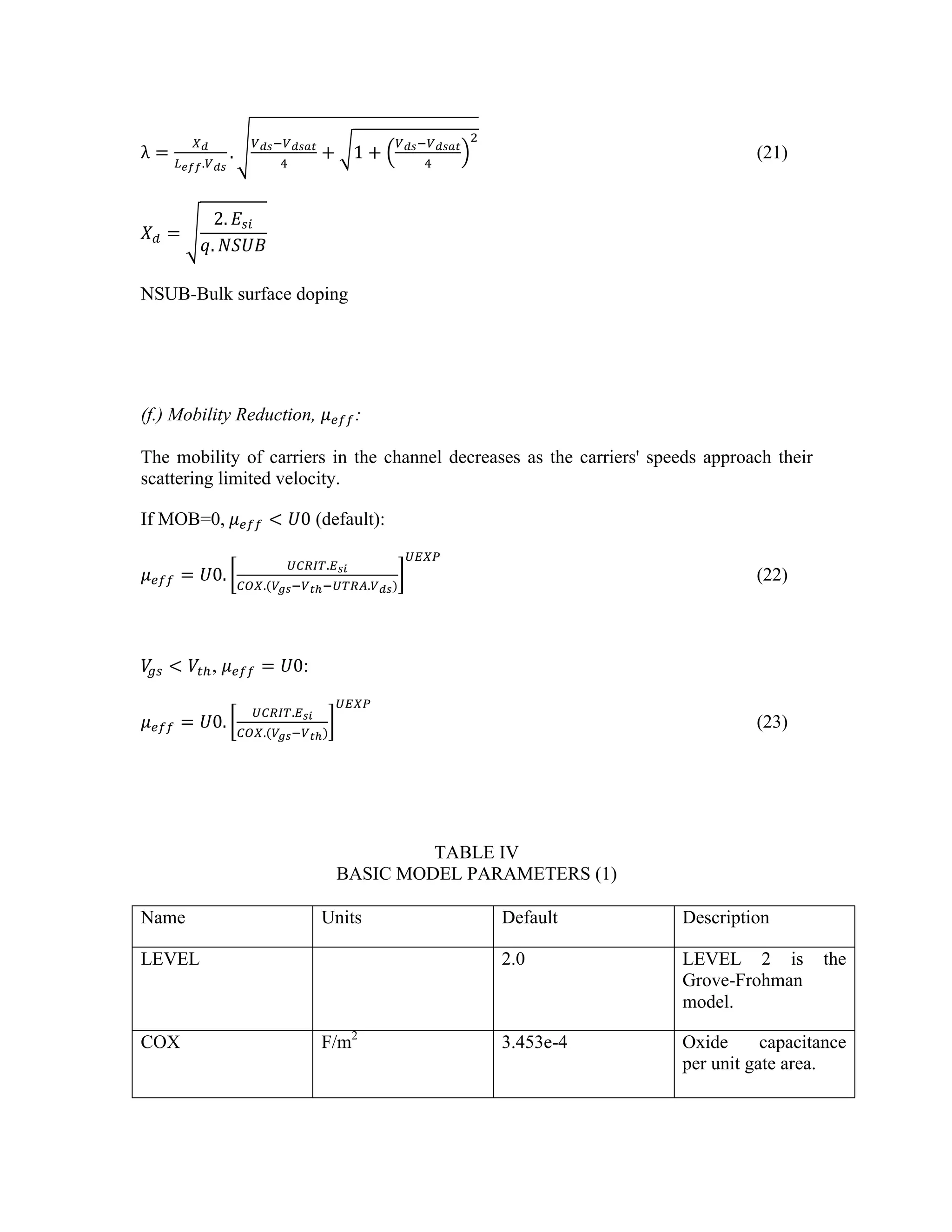
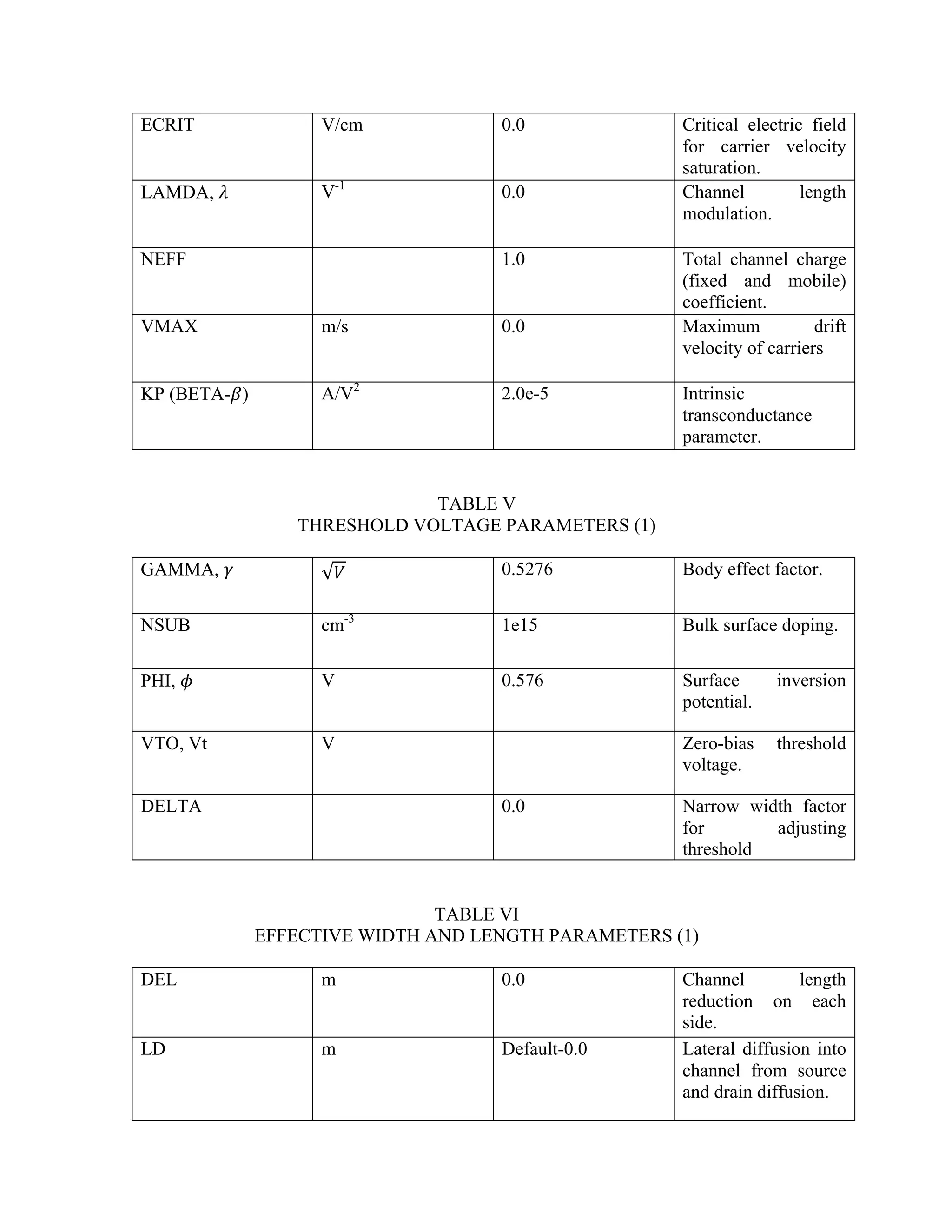
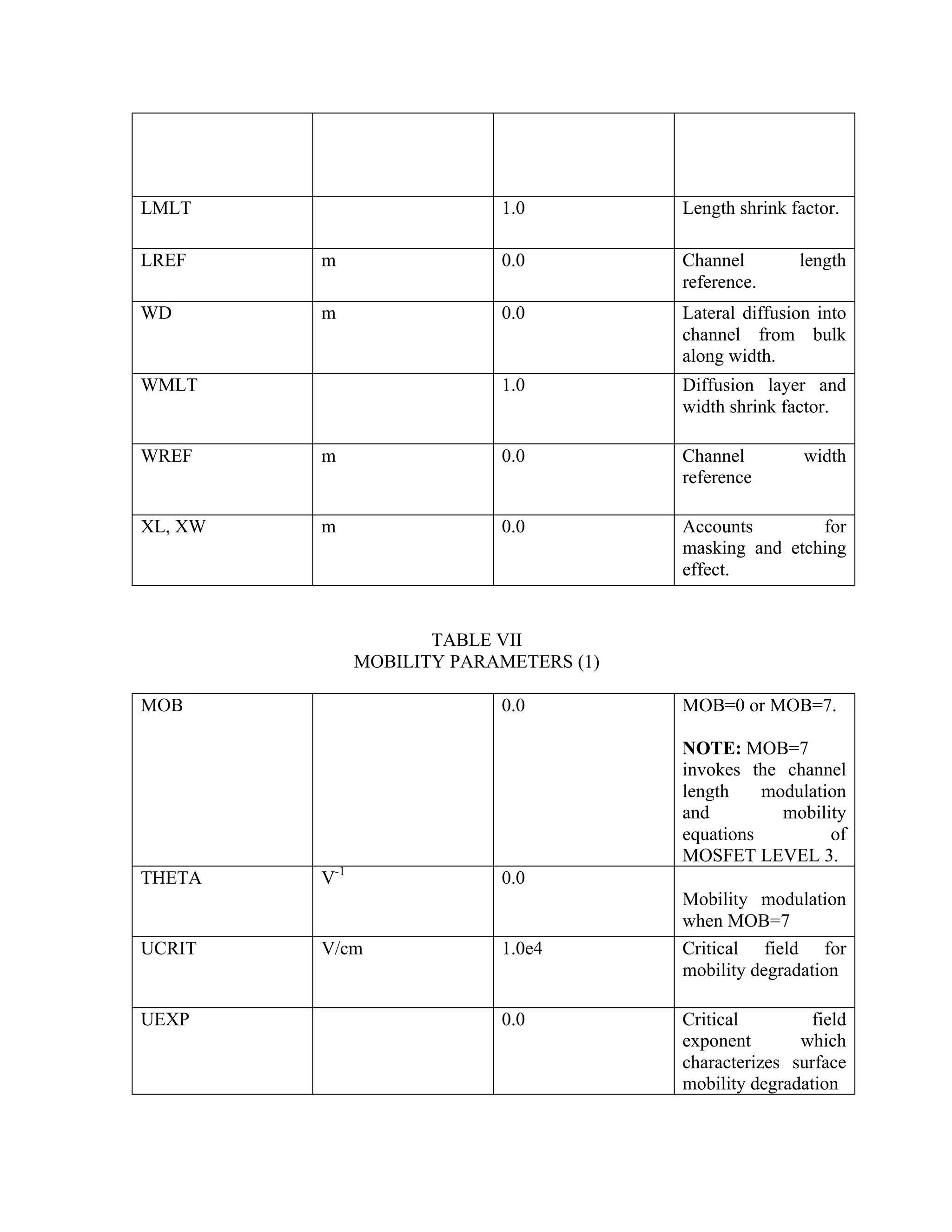
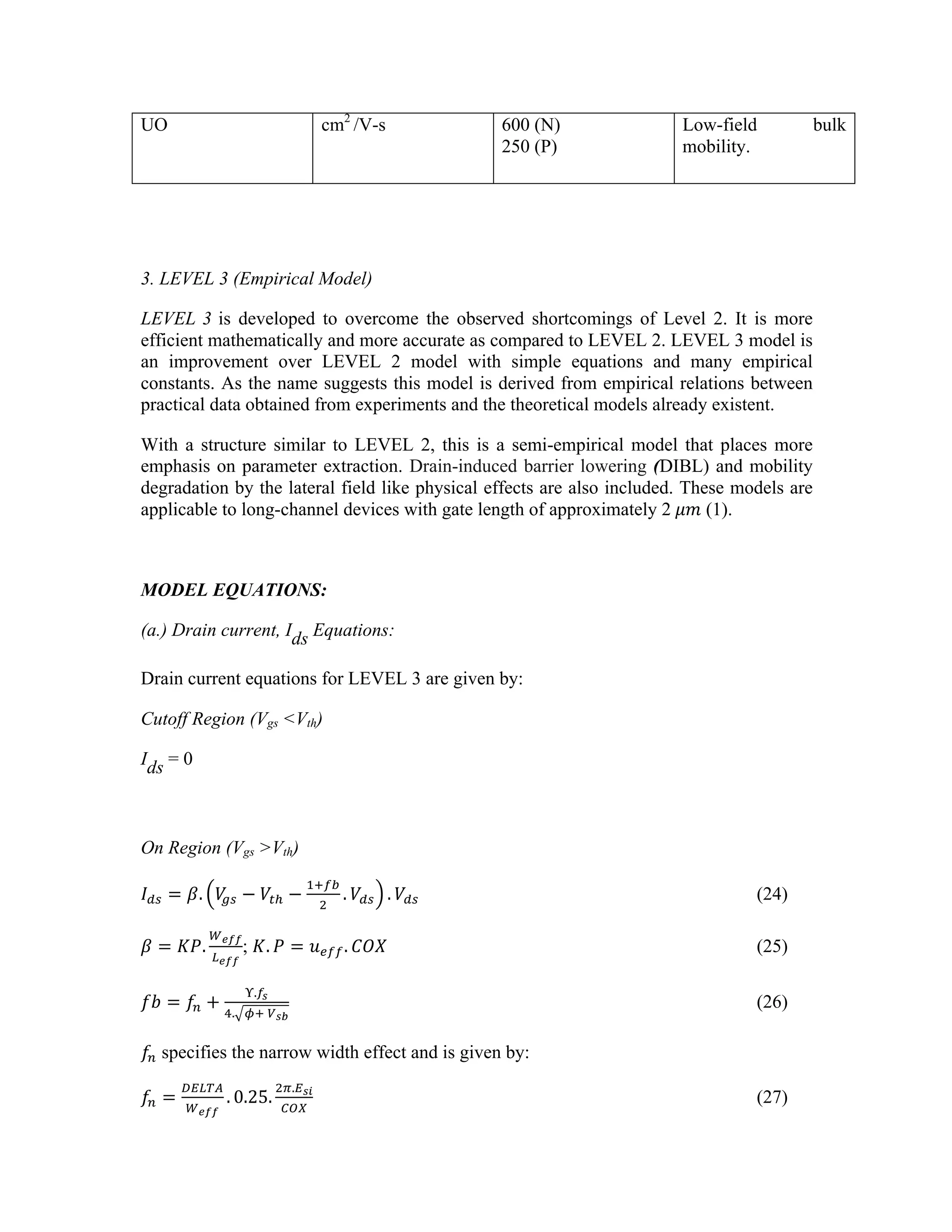
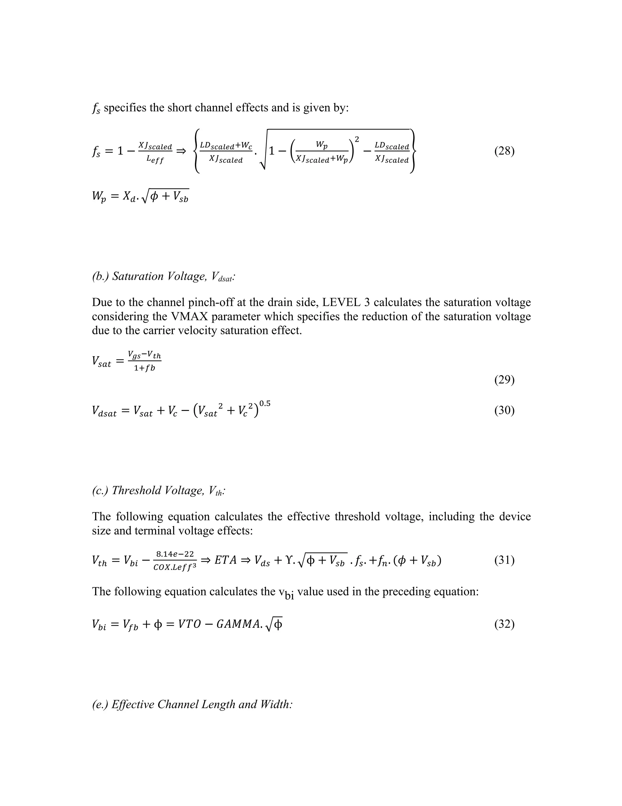
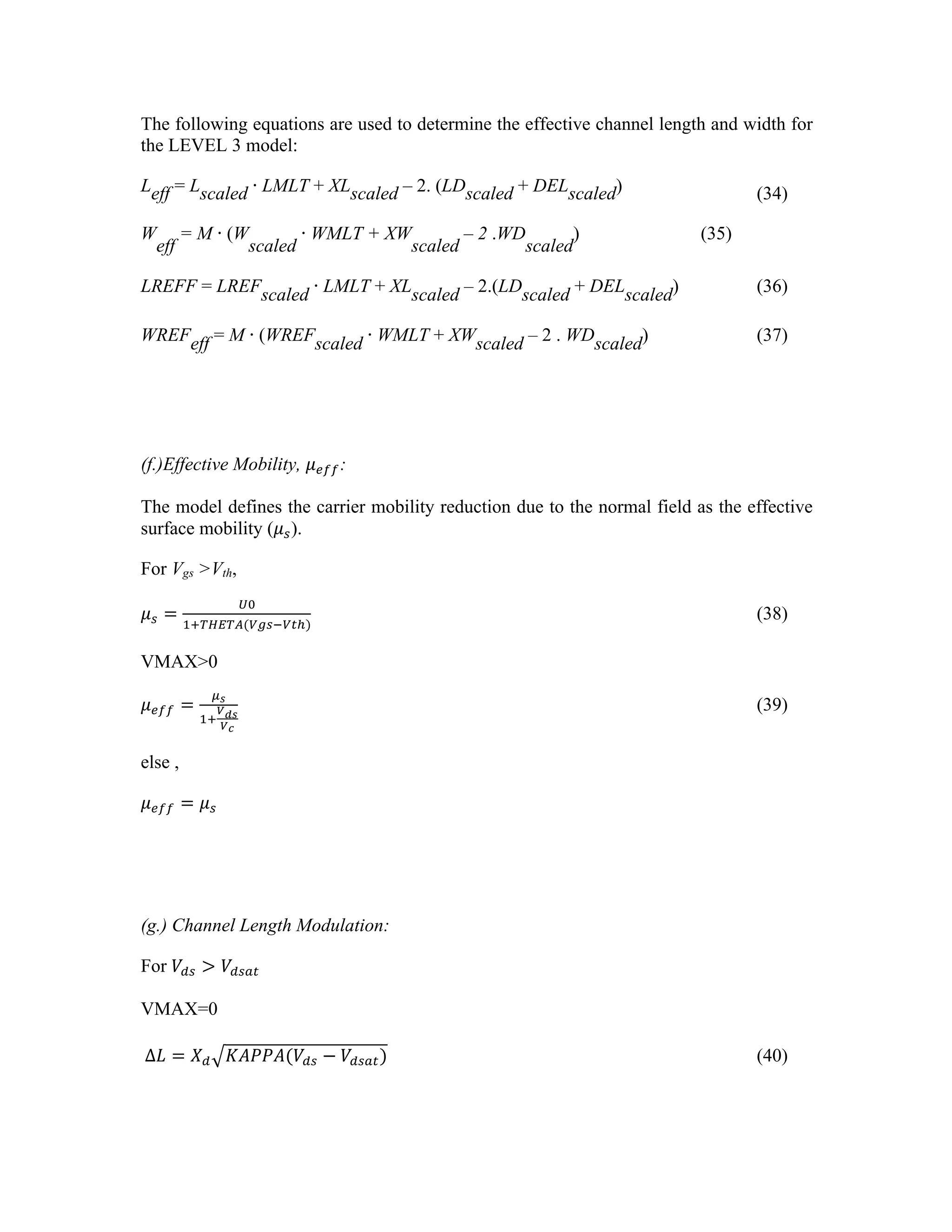
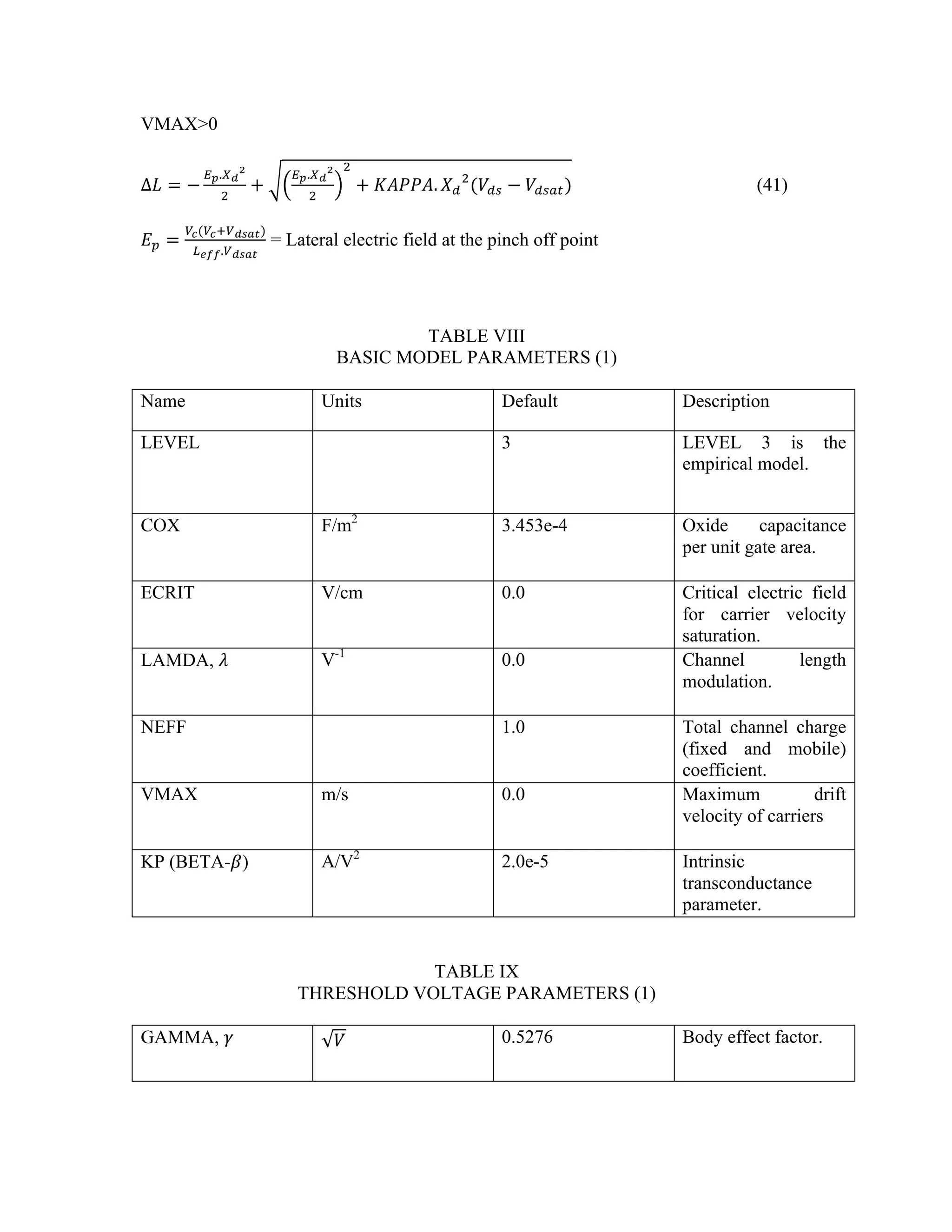
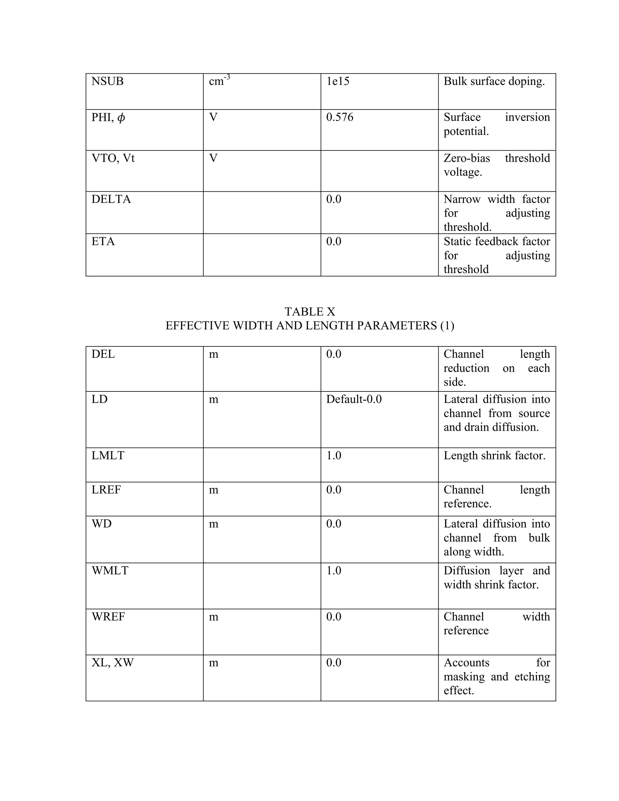
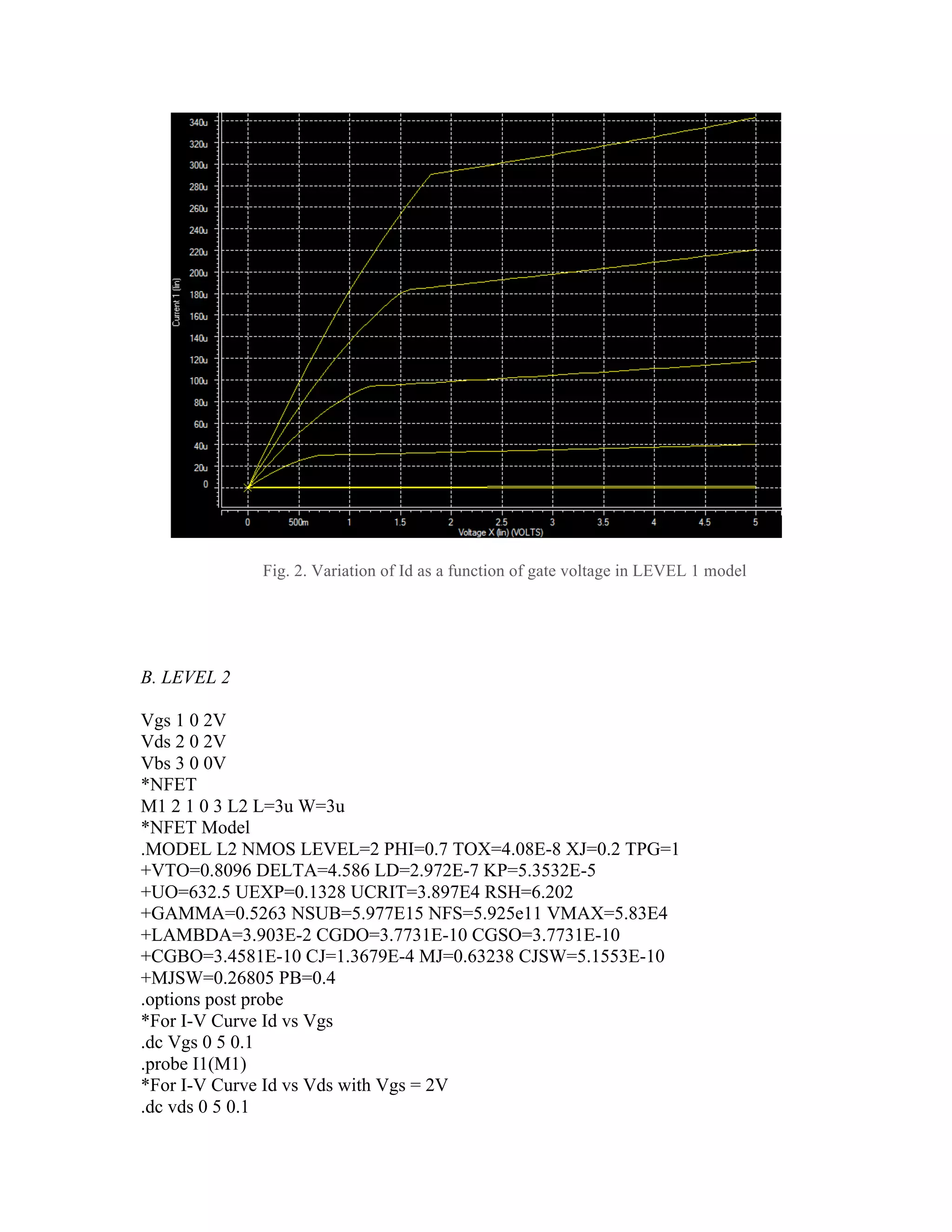
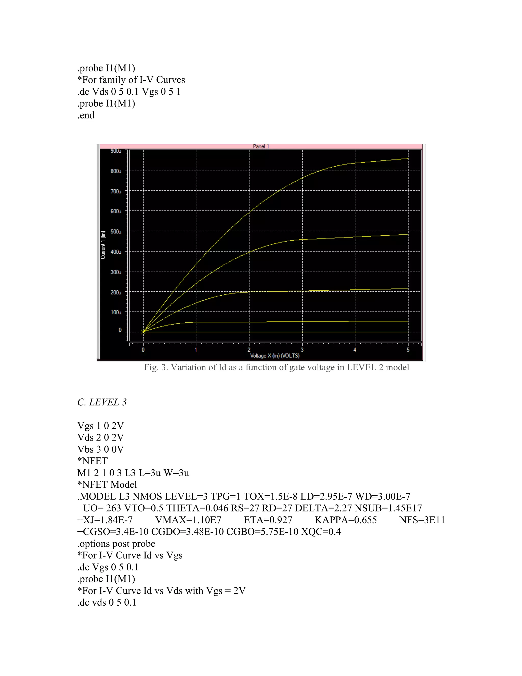
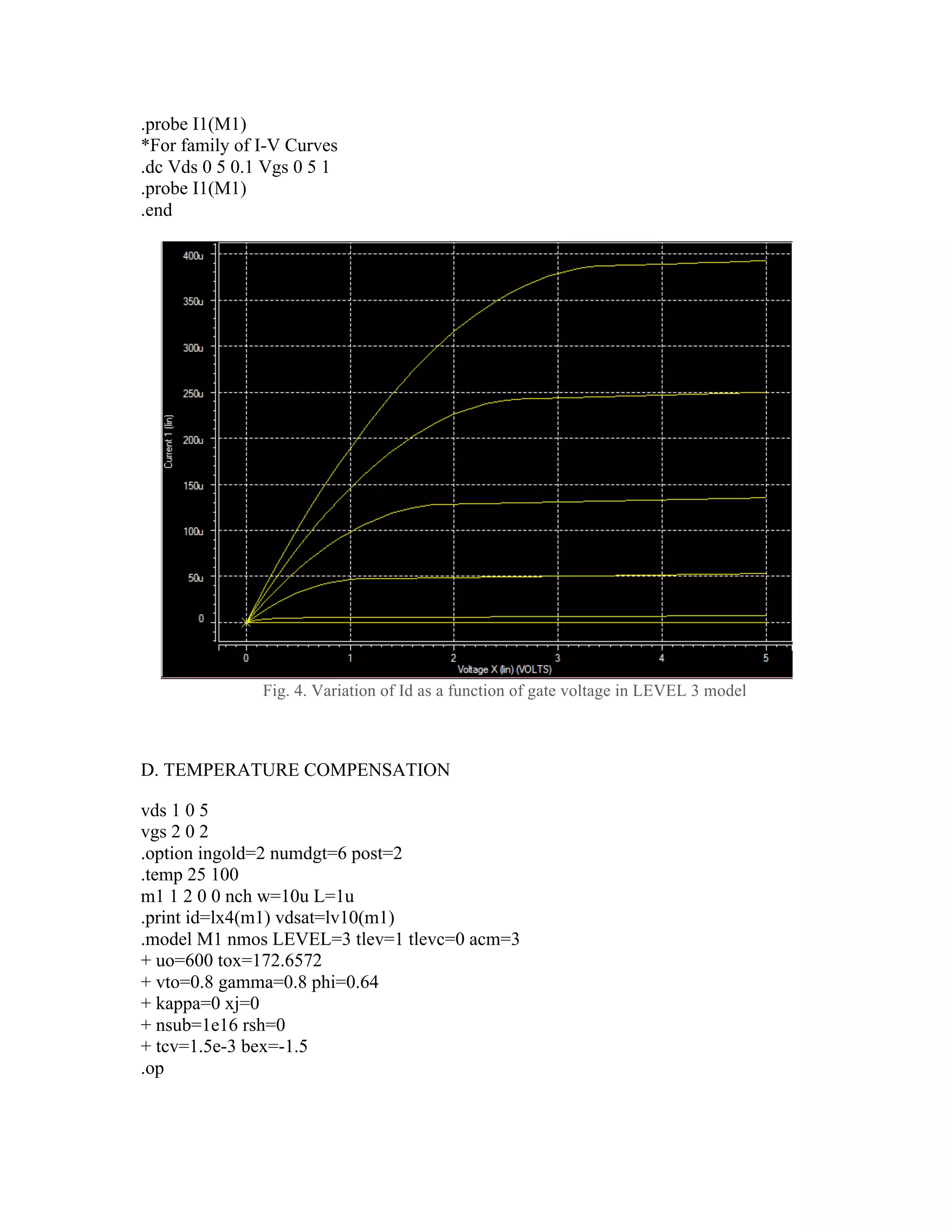
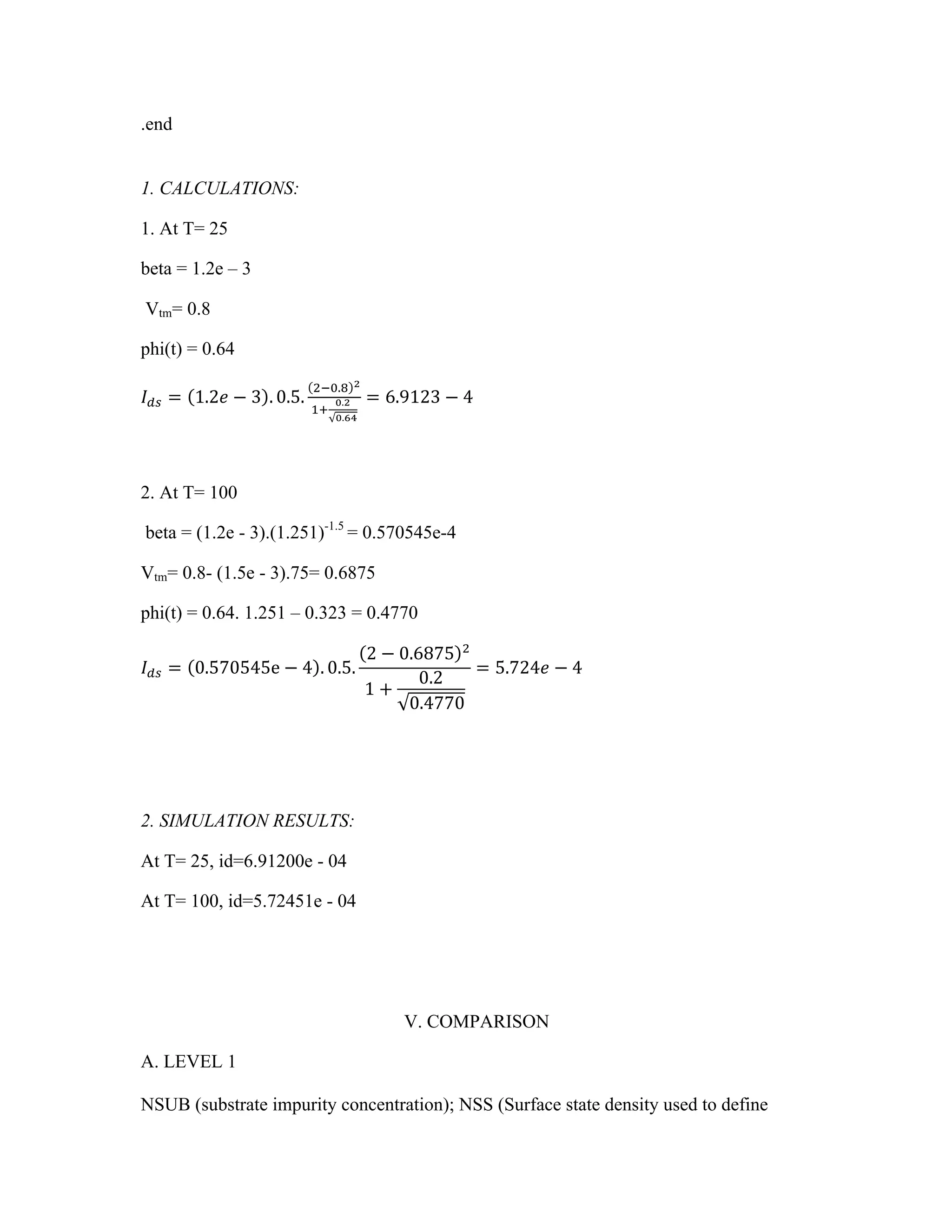
This document compares level 1, 2, and 3 MOSFET models in SPICE simulations. It provides background on device modeling and outlines the key equations that define each model level. Level 1 is the simplest model and does not account for short channel effects. Level 2 includes mobility degradation and threshold voltage variations. Level 3 has similar accuracy to level 2 but faster simulation time and better convergence. Drain current versus drain-source voltage characteristics are plotted to show differences between the models.
![Comparison of Level 1, 2 and 3 MOSFET’s
Twesha Patel
Course: Advanced Electronics, Instructor: Prof. Alan Davis, Semester: Fall 2014,
Department of Electrical Engineering, The University of Texas, Arlington
(Dated: December 3, 2014)
Abstract- The scaling of MOS technology to nanometer sizes leads to the
development of physical and predictive models for circuit simulation that cover AC,
RF, DC, temperature, geometry, bias and noise characteristics (1). This paper
addresses the comparison between level 1,2 and 3 MOSFETs. The results are
examined using SPICE (Simulation Program with Integrated Circuit Emphasis).
Drain current versus drain-source voltage characteristics are plotted to display the
differences between them.
I. INTRODUCTION
The downscaling of transistor dimensions over the past years is an evolutionary process
to provide superior performance, reduced size and cost. To assist this miniaturization of
devices, new simulators and device models have been invented.
Everywhere from designing of an IC, manufacturing to fabrication technology
development, modeling of device plays a major role in the advancement of Metal oxide
semiconductor technology. Considering the real time effects is essential while simulating
these device models. The SPICE model uses variety of parasitic circuit elements and
some process related parameters. The circuit designer can control these parameters and
syntax for MOSFET is given by
. MODEL <model name> NMOS [model parameters]
. MODEL <model name> PMOS [model parameters]
II. DEVICE MODELLING
To describe the performance of a device in mathematical terms, device modeling can be
used. Theoretical or empirical considerations, or both can be used to derive a model. A
few parameters along with the characterization can be used to build a desired model.
Quality of approximation and its complexity are often traded while establishing a model
making procedure. When making these tradeoffs, an engineer considers factors such as
intended use of the model and the required accuracy.](https://image.slidesharecdn.com/mosfetmodeling-220416114225/75/MOSFET_MODELING-PDF-2-2048.jpg)
![detailed description.
2. LEVEL 2 model-The bulk charge effects on current are considered in this model.
3. LEVEL 3 model-The accuracy of this model is similar to that of LEVEL 2 but it offers
lesser simulation time and has a greater tendency to converge.
Fig. 1. Schematic of Level 1,2 and 3 MOSFET’s (4)
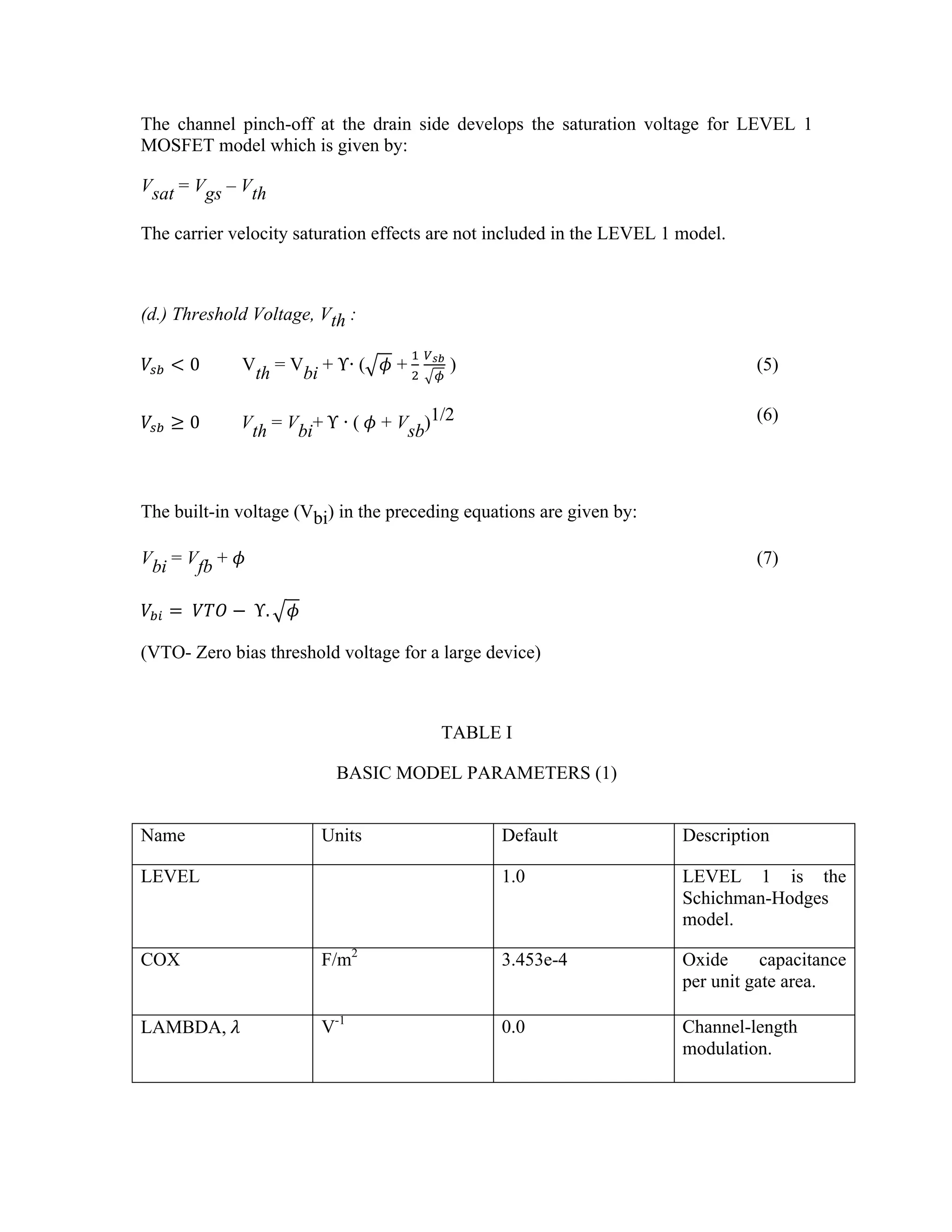
1. LEVEL 1 (Schichman-Hodges Model)
The model is applicable to devices with gate length greater than 10𝜇𝑚. This model is a
first order approximation of practical output of long channel MOS device. This model
takes into consideration channel length modulation by using a parameter L and body bias
effect is taken care by the transconductance. Whenever the channel length reduces below
4 mm, these parameters become dependent on externally applied voltages and other
parameters. The drain current (Ids) values will be lesser than the practically obtained
values if the channel length falls below this value and the model fails to include the
parameters related to short and narrow channel effects (3).
Gradual channel approximation and the square law for the saturated drain current are the
simplifications employed in this model (1).
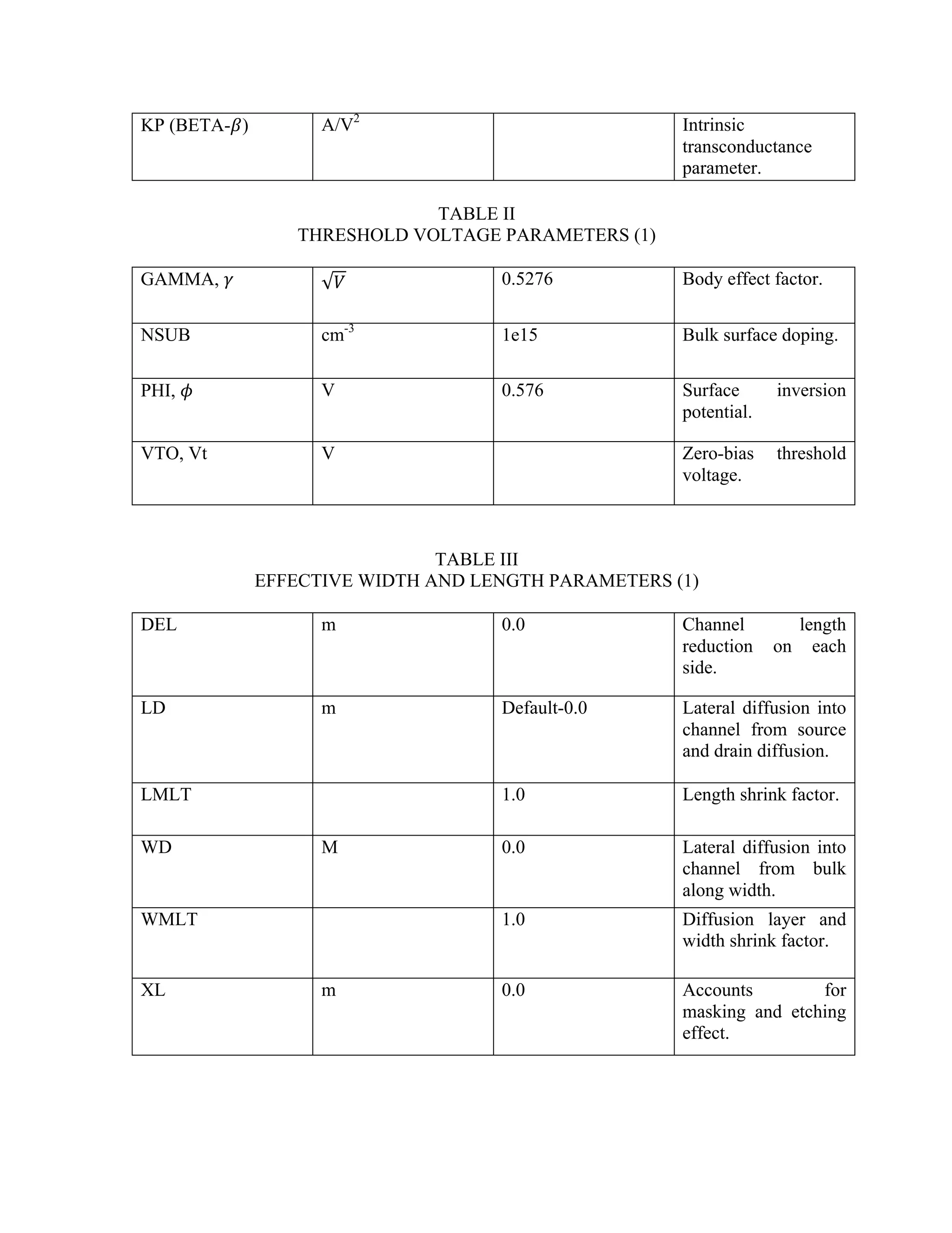
MODEL EQUATIONS:
(a.) Drain current, Ids Equations:
174
Examples M1 14 2 13 0 PNOM L=25u W=12u
M13 15 3 0 0 PSTRONG
M16 17 3 0 0 PSTRONG M=2
M28 0 2 100 100 NWEAK L=33u W=12u
+ AD=288p AS=288p PD=60u PS=60u NRD=14 NRS=24 NRG=10
Model form .MODEL <model name> NMOS [model parameters]
.MODEL <model name> PMOS [model parameters]
Description The MOSFET is modeled as an intrinsic MOSFET using ohmic resistances in se
drain, source, gate, and bulk (substrate). There is also a shunt resistance (RDS) i
with the drain-source channel.
Arguments and options
L and W
are the channel length and width, which are decreased to get the effective ch
length and width. They can be specified in the device, .MODEL (model de
.OPTIONS (analysis options) statements. The value in the device statemen
the value in the model statement, which supersedes the value in the .OPTION
Defaults for L and W can be set in the .OPTIONS statement. If L or W defa
set, their default value is 100 u.
[L=<value>] [W=<value>] cannot be used in conjunction with Mon
analysis.
Drain
RD
Cgb
Cgd Cbd
RB
Bulk
Idrain
Cbs
Cgs
RG
Gate
Source
RS](https://image.slidesharecdn.com/mosfetmodeling-220416114225/75/MOSFET_MODELING-PDF-4-2048.jpg)
![encompass constantly downscaling technologies. Now a huge emphasis is placed on
obtaining physics-based, simple and highly accurate analytical device models.
REFERENCES
[1] HSPICE® Reference Manual: MOSFET Models Version D-2010.12, December 2010
[2] SPICE Modeling of MOSFETs in Deep Submicron, GEORGE ANGELOV, MARLN
HRISTOV, Technical University of Sofia, Faculty f Electronic Engineering and Technology, ECAD
Laboratory.
[3] H. Shichman and D. A. Hodges, “Modeling and simulation of insulated-gate field-
effect transistor switching circuits,” IEEE Journal of Solid-State Circuits, SC-3, 285,
September 1968.
[4] ORCAD SPICE A/D Reference Manual, Version 9.0, October 1998.
View publication stats
View publication stats](https://image.slidesharecdn.com/mosfetmodeling-220416114225/75/MOSFET_MODELING-PDF-26-2048.jpg)


