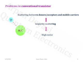
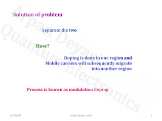
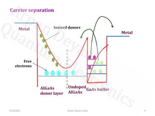
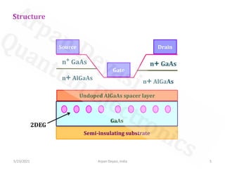
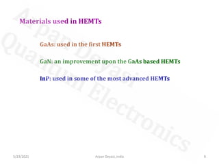
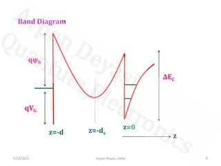
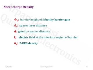
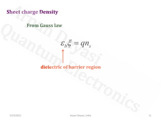
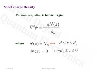
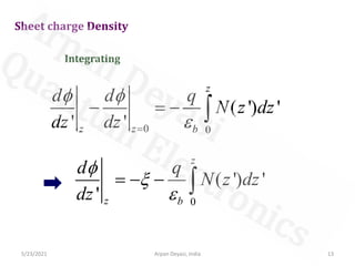
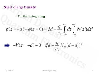
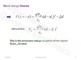
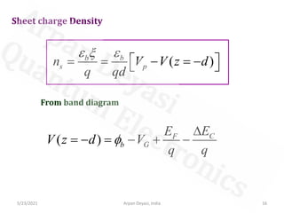
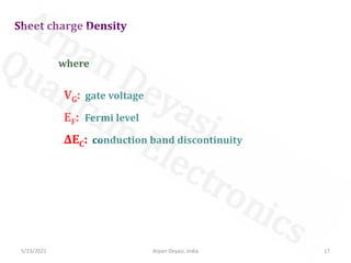
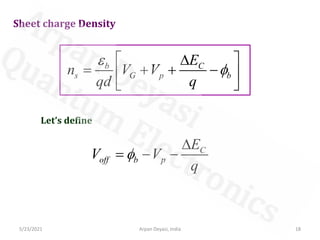
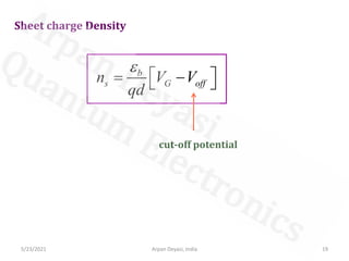
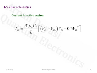
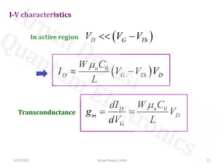
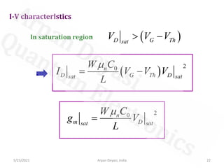
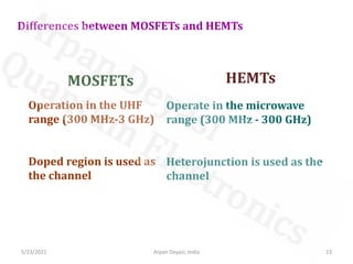
1. High Electron Mobility Transistor
Arpan Deyasi
RCCIIT, India
5/23/2021 1
Arpan Deyasi, India
2. 5/23/2021 2
Arpan Deyasi, India
Problems in conventional transistor
D
Scattering between donors/acceptors and mobile carriers
Impurity scattering
High noise
M.C
3. 5/23/2021 3
Arpan Deyasi, India
Solution of problem
Separate the two
How?
Doping is done in one region and
Mobile carriers will subsequently migrate
into another region
Process is known as modulation doping
4. 5/23/2021 4
Arpan Deyasi, India
Carrier separation
Metal
GaAs buffer
AlGaAs
donor layer
Undoped
AlGaAs
Metal Ionized donors
Free
electrons
6. Characteristics of HEMT
mobility of free carriers are very high due to suppressed
ionized impurity scattering which makes very low
gate-to-source resistance
carrier freezeout problem is not present at extremely
low temperature because of electrons presence in a
region of energy below donor levels in high bandgap
material. So the device is treated as high-gain, low-noise one
5/23/2021 6
Arpan Deyasi, India
7. Characteristics of HEMT
Using materials with higher conduction band discontinuity,
large device transconductance can be obtained
Because of smaller active channel, it can be operated at
lower temperature
5/23/2021 7
Arpan Deyasi, India
8. 5/23/2021 Arpan Deyasi, India 8
Materials used in HEMTs
InP: used in some of the most advanced HEMTs
GaAs: used in the first HEMTs
GaN: an improvement upon the GaAs based HEMTs
10. Φb: barrier height of Schottky barrier gate
ds: spacer layer distance
d: gate-to-channel distance
ξ: electric field at the interface region of barrier
ns: 2-DEG density
Sheet charge Density
5/23/2021 10
Arpan Deyasi, India
11. Sheet charge Density
From Gauss law
b s
qn
=
dielectric of barrier region
5/23/2021 11
Arpan Deyasi, India
12. Sheet charge Density
Poisson’s equation is barrier region
2 ( )
b
qN z
= −
where ( ) D
N z N
= s
d z d
−
( ) 0
N z = 0
s
d z
−
5/23/2021 12
Arpan Deyasi, India
13. Sheet charge Density
Integrating
0 0
( ') '
' '
z
z z b
d d q
N z dz
dz dz
=
− = −
0
( ') '
'
z
z b
d q
N z dz
dz
= − −
5/23/2021 13
Arpan Deyasi, India
14. Sheet charge Density
Further integrating
( ) ( 0) ( ') '
d d
b ds ds
q
z d z d dz N z dz
− −
− −
= − − = = −
2
( ) 0 ( )
D s
b
q
V z d d N d d
− = − − = − −
5/23/2021 14
Arpan Deyasi, India
15. Sheet charge Density
2
( ) ( )
D
s
b
qN
V z d d d d
= − = − −
Let’s define 2
( )
D
p s
b
qN
V d d
= −
This is the necessary voltage to pinch-off the doped
AlxGa1-xAs layer
5/23/2021 15
Arpan Deyasi, India
16. Sheet charge Density
( )
b b
s p
n V V z d
q qd
= = − = −
From band diagram
( ) C
F
b G
E
E
V z d V
q q
= − = − + −
5/23/2021 16
Arpan Deyasi, India
17. Sheet charge Density
where
VG: gate voltage
EF: Fermi level
ΔEC: conduction band discontinuity
5/23/2021 17
Arpan Deyasi, India
18. Sheet charge Density
b C
s G p b
E
n V V
qd q
= + + −
Let’s define
C
off b p
E
V V
q
= − −
5/23/2021 18
Arpan Deyasi, India
19. Sheet charge Density
b
s G off
n V V
qd
= −
cut-off potential
5/23/2021 19
Arpan Deyasi, India
20. 5/23/2021 Arpan Deyasi, India 20
I-V characteristics
Current in active region
( ) 2
0
0.5
n
D G Th D D
W C
I V V V V
L
= − −
21. 5/23/2021 Arpan Deyasi, India 21
I-V characteristics
In active region ( )
D G Th
V V V
−
( )
0
n
D G Th D
W C
I V V V
L
−
Transconductance
0
n
D
m D
G
W C
dI
g V
dV L
= =
22. 5/23/2021 Arpan Deyasi, India 22
I-V characteristics
In saturation region ( )
D G Th
sat
V V V
−
( )
2
0
n
D G Th D
sat sat
W C
I V V V
L
= −
2
0
n
m D
sat sat
W C
g V
L
=
23. 5/23/2021 Arpan Deyasi, India 23
Differences between MOSFETs and HEMTs
MOSFETs
Operation in the UHF
range (300 MHz-3 GHz)
Doped region is used as
the channel
HEMTs
Operate in the microwave
range (300 MHz - 300 GHz)
Heterojunction is used as the
channel
24. 5/23/2021 Arpan Deyasi, India 24
Applications
Power electronics
Precision sensors
Next generation wired/wireless communication
Advanced radars
25. 5/23/2021 Arpan Deyasi, India 25
Areas to be covered in future
New structures need to be developed to reduce parasitic
capacitance and address the failure mechanisms
Reliability of GaN and InP HEMT’s are excellent at lower
frequencies
Reliability issues need to be resolved in GaN and InP
HEMT’s at higher frequencies
Failure mechanisms such as gate sinking, thermal
degradation of ohmic contact, and charge trapping needs
further investigation