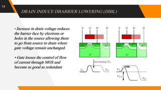
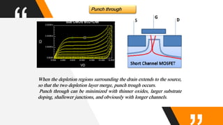
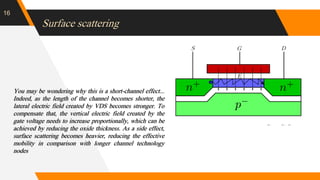
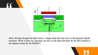
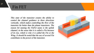
Short Channel Effects are governed by complex physical phenomena and mainly Influenced because of both vertical and horizontal electric field components.
To meet the current requirements of
Electronic devices, the miniaturization of devices is important. And so is Second Order effects which otherwise degrade the performance of devices.
Here are the all short channel effects that you require.It consist of:-
Drain Induced Barrier Lowering
Hot electron Effect
Impact Ionization
Surface Scattering
Velocity saturation
In electronics, short-channel effects occur in MOSFETs in which the channel length is comparable to the depletion layer widths of the source and drain junctions. These effects include, in particular, drain-induced barrier lowering, velocity saturation, Quantum confinement and hot carrier degradation
SHORT-CHANNEL EFFECTS
A MOSFET is considered to be short when the channel length ‘L’ is the same order of magnitude as the depletion-layer widths (xdD, xdS). The potential distribution in the channel now depends upon both, transverse field Ex, due to gate bias and also on the longitudinal field Ey, due to drain bias When the Gate channel length <<1 m, short channel effect becomes important .
This leads to many
undesirable effects in MOSFET.
The short-channel effects are attributed to two physical phenomena:
A) The limitation imposed on electron drift characteristics in the channel,
B) The modification of the threshold voltage due to the shortening channel length.
In particular five different short-channel effects can be distinguished:
1. Drain-induced barrier lowering and “Punch through”
2. Surface scattering
3. Velocity saturation
4. Impact ionization
5. Hot electrons
Threshold Voltage & Channel Length ModulationBulbul Brahma
Design and Technology of Electronic Devices:
Review of microelectronic devices, introduction to MOS technology and related devices.
MOS transistor theory, scaling theory related to MOS circuits, short channel effect and its
consequences, narrow width effect, FN tunnelling, Double gate MOSFET, Cylindrical
MOSFET, Basic concept of CMOS circuits and logic design. Circuit characterization and
performance estimation, important issues in real devices. PE logic, Domino logic, Pseudo
N-MOS logic-dynamic CMOS and Clocking, layout design and stick diagram, CMOS
analog circuit design, CMOS design methods. Introduction to SOI, Multi layer circuit
design and 3D integration. CMOS processing technology: Crystal grown and Epitaxy, Film
formation, Lithography and Etching, Impurity doping, Integrated Devices.
In MOS, source-drain regions of adjacent MOS transistors together with interconnection metal lines may constitute parasitic MOS transistors unless they are isolated from each other. Hence, each MOSFET must be electrically isolated from each other. Device Isolation Techniques in VLSI microfabrication of MOS are discussed.
Analytical Modeling of Tunneling Field Effect Transistor (TFET)Abu Obayda
Tunneling Field-Effect Transistor (TFET) has emerged as an alternative for conventional CMOS by enabling the supply voltage, VDD, scaling in ultra-low power, energy efficient computing, due to its sub-60 mV/decade sub-threshold slope (SS). Given its unique device characteristics such as the asymmetrical source/drain design induced unidirectional conduction, enhanced on-state Miller capacitance effect and steep switching at low voltages, TFET based circuit design requires strong interactions between the device-level and the circuit-level to explore the performance benefits, with certain modifications of the conventional CMOS circuits to achieve the functionality and optimal energy efficiency. Because TFET operates at low supply voltage range (VDD<0.5V) to outperform CMOS, reliability issues can have profound impact on the circuit design from the practical application perspective. In this thesis report, we have analyzed the drain current characteristics of TFET with respect channel length. From our simulation result, it is observed that the drain current is minimum with respect to increasing channel length for Si and the drain current decreases for all the materials when the channel length is increased and after normalization lowest value of drain current is got for 10nm channel length.
Reduced channel length cause departures from long channel behaviour as two-dimensional potential distribution and high electric fields give birth to Short channel effects.
Design of Near-Threshold CMOS Logic GatesVLSICS Design
Numerous efforts have made to balance the tradeoff between power consumption, area and speed of a design. While studying the design at the two extreme ends of the design spectrum, namely the ultra-low power with acceptable performance at one end and high performance with power within limit at the other has not made. One solution to achieve the ultra-low power consumption is to operate the design in subthreshold region. The use of sub-threshold circuit designing in fast and energy efficient circuits is always needed in electronics industry especially in DSP, image processing and arithmetic units in microprocessors, where the low power is the primary concern and the delay can be tolerated. We design a simple CMOS inverter in weak inversion region (sub-threshold) and compare the power consumption with strong inversion region using Cadence 0.18µm Technology.
DESIGN OF DIFFERENT DIGITAL CIRCUITS USING SINGLE ELECTRON DEVICESmsejjournal
Single Electron transistor (SET) is foreseen as an excellently growing technology. The aim of this paper is
to present in short the fundamentals of SET as well as to realize its application in the design of single
electron device based novel digital logic circuits with the help of a Monte Carlo based simulator. A Single
Electron Transistors (SET) is characterized by two most substantial determinants. One is very low power
dissipation while the other is its small stature that makes it a favorable suitor for the future generation of
very high level integration. With the utilization of SET, technology is moving past CMOS age resulting in
power efficient, high integrity, handy and high speed devices. Conducting a check on the transport of single
electrons is one of the most stirring aspects of SET technologies. Apparently, Monte Carlo technique is in
vogue in terms of simulating SED based circuits. Hence, a MC based tool called SIMON 2.0 is exercised
upon for the design and simulation of these digital logic circuits. Further, an efficient functioning of the
logic circuits such as multiplexers, decoders, adders and converters are illustrated and established by
means of circuit simulation using SIMON 2.0 simulator.
LF Energy Webinar: Electrical Grid Modelling and Simulation Through PowSyBl -...DanBrown980551
Do you want to learn how to model and simulate an electrical network from scratch in under an hour?
Then welcome to this PowSyBl workshop, hosted by Rte, the French Transmission System Operator (TSO)!
During the webinar, you will discover the PowSyBl ecosystem as well as handle and study an electrical network through an interactive Python notebook.
PowSyBl is an open source project hosted by LF Energy, which offers a comprehensive set of features for electrical grid modelling and simulation. Among other advanced features, PowSyBl provides:
- A fully editable and extendable library for grid component modelling;
- Visualization tools to display your network;
- Grid simulation tools, such as power flows, security analyses (with or without remedial actions) and sensitivity analyses;
The framework is mostly written in Java, with a Python binding so that Python developers can access PowSyBl functionalities as well.
What you will learn during the webinar:
- For beginners: discover PowSyBl's functionalities through a quick general presentation and the notebook, without needing any expert coding skills;
- For advanced developers: master the skills to efficiently apply PowSyBl functionalities to your real-world scenarios.
Key Trends Shaping the Future of Infrastructure.pdfCheryl Hung
Keynote at DIGIT West Expo, Glasgow on 29 May 2024.
Cheryl Hung, ochery.com
Sr Director, Infrastructure Ecosystem, Arm.
The key trends across hardware, cloud and open-source; exploring how these areas are likely to mature and develop over the short and long-term, and then considering how organisations can position themselves to adapt and thrive.
Software Delivery At the Speed of AI: Inflectra Invests In AI-Powered QualityInflectra
In this insightful webinar, Inflectra explores how artificial intelligence (AI) is transforming software development and testing. Discover how AI-powered tools are revolutionizing every stage of the software development lifecycle (SDLC), from design and prototyping to testing, deployment, and monitoring.
Learn about:
• The Future of Testing: How AI is shifting testing towards verification, analysis, and higher-level skills, while reducing repetitive tasks.
• Test Automation: How AI-powered test case generation, optimization, and self-healing tests are making testing more efficient and effective.
• Visual Testing: Explore the emerging capabilities of AI in visual testing and how it's set to revolutionize UI verification.
• Inflectra's AI Solutions: See demonstrations of Inflectra's cutting-edge AI tools like the ChatGPT plugin and Azure Open AI platform, designed to streamline your testing process.
Whether you're a developer, tester, or QA professional, this webinar will give you valuable insights into how AI is shaping the future of software delivery.
UiPath Test Automation using UiPath Test Suite series, part 4DianaGray10
Welcome to UiPath Test Automation using UiPath Test Suite series part 4. In this session, we will cover Test Manager overview along with SAP heatmap.
The UiPath Test Manager overview with SAP heatmap webinar offers a concise yet comprehensive exploration of the role of a Test Manager within SAP environments, coupled with the utilization of heatmaps for effective testing strategies.
Participants will gain insights into the responsibilities, challenges, and best practices associated with test management in SAP projects. Additionally, the webinar delves into the significance of heatmaps as a visual aid for identifying testing priorities, areas of risk, and resource allocation within SAP landscapes. Through this session, attendees can expect to enhance their understanding of test management principles while learning practical approaches to optimize testing processes in SAP environments using heatmap visualization techniques
What will you get from this session?
1. Insights into SAP testing best practices
2. Heatmap utilization for testing
3. Optimization of testing processes
4. Demo
Topics covered:
Execution from the test manager
Orchestrator execution result
Defect reporting
SAP heatmap example with demo
Speaker:
Deepak Rai, Automation Practice Lead, Boundaryless Group and UiPath MVP
UiPath Test Automation using UiPath Test Suite series, part 3DianaGray10
Welcome to UiPath Test Automation using UiPath Test Suite series part 3. In this session, we will cover desktop automation along with UI automation.
Topics covered:
UI automation Introduction,
UI automation Sample
Desktop automation flow
Pradeep Chinnala, Senior Consultant Automation Developer @WonderBotz and UiPath MVP
Deepak Rai, Automation Practice Lead, Boundaryless Group and UiPath MVP
The Art of the Pitch: WordPress Relationships and SalesLaura Byrne
Clients don’t know what they don’t know. What web solutions are right for them? How does WordPress come into the picture? How do you make sure you understand scope and timeline? What do you do if sometime changes?
All these questions and more will be explored as we talk about matching clients’ needs with what your agency offers without pulling teeth or pulling your hair out. Practical tips, and strategies for successful relationship building that leads to closing the deal.
Slack (or Teams) Automation for Bonterra Impact Management (fka Social Soluti...Jeffrey Haguewood
Sidekick Solutions uses Bonterra Impact Management (fka Social Solutions Apricot) and automation solutions to integrate data for business workflows.
We believe integration and automation are essential to user experience and the promise of efficient work through technology. Automation is the critical ingredient to realizing that full vision. We develop integration products and services for Bonterra Case Management software to support the deployment of automations for a variety of use cases.
This video focuses on the notifications, alerts, and approval requests using Slack for Bonterra Impact Management. The solutions covered in this webinar can also be deployed for Microsoft Teams.
Interested in deploying notification automations for Bonterra Impact Management? Contact us at sales@sidekicksolutionsllc.com to discuss next steps.
Smart TV Buyer Insights Survey 2024 by 91mobiles.pdf91mobiles
91mobiles recently conducted a Smart TV Buyer Insights Survey in which we asked over 3,000 respondents about the TV they own, aspects they look at on a new TV, and their TV buying preferences.
Accelerate your Kubernetes clusters with Varnish CachingThijs Feryn
A presentation about the usage and availability of Varnish on Kubernetes. This talk explores the capabilities of Varnish caching and shows how to use the Varnish Helm chart to deploy it to Kubernetes.
This presentation was delivered at K8SUG Singapore. See https://feryn.eu/presentations/accelerate-your-kubernetes-clusters-with-varnish-caching-k8sug-singapore-28-2024 for more details.
Transcript: Selling digital books in 2024: Insights from industry leaders - T...BookNet Canada
The publishing industry has been selling digital audiobooks and ebooks for over a decade and has found its groove. What’s changed? What has stayed the same? Where do we go from here? Join a group of leading sales peers from across the industry for a conversation about the lessons learned since the popularization of digital books, best practices, digital book supply chain management, and more.
Link to video recording: https://bnctechforum.ca/sessions/selling-digital-books-in-2024-insights-from-industry-leaders/
Presented by BookNet Canada on May 28, 2024, with support from the Department of Canadian Heritage.
Builder.ai Founder Sachin Dev Duggal's Strategic Approach to Create an Innova...Ramesh Iyer
In today's fast-changing business world, Companies that adapt and embrace new ideas often need help to keep up with the competition. However, fostering a culture of innovation takes much work. It takes vision, leadership and willingness to take risks in the right proportion. Sachin Dev Duggal, co-founder of Builder.ai, has perfected the art of this balance, creating a company culture where creativity and growth are nurtured at each stage.
Essentials of Automations: Optimizing FME Workflows with ParametersSafe Software
Are you looking to streamline your workflows and boost your projects’ efficiency? Do you find yourself searching for ways to add flexibility and control over your FME workflows? If so, you’re in the right place.
Join us for an insightful dive into the world of FME parameters, a critical element in optimizing workflow efficiency. This webinar marks the beginning of our three-part “Essentials of Automation” series. This first webinar is designed to equip you with the knowledge and skills to utilize parameters effectively: enhancing the flexibility, maintainability, and user control of your FME projects.
Here’s what you’ll gain:
- Essentials of FME Parameters: Understand the pivotal role of parameters, including Reader/Writer, Transformer, User, and FME Flow categories. Discover how they are the key to unlocking automation and optimization within your workflows.
- Practical Applications in FME Form: Delve into key user parameter types including choice, connections, and file URLs. Allow users to control how a workflow runs, making your workflows more reusable. Learn to import values and deliver the best user experience for your workflows while enhancing accuracy.
- Optimization Strategies in FME Flow: Explore the creation and strategic deployment of parameters in FME Flow, including the use of deployment and geometry parameters, to maximize workflow efficiency.
- Pro Tips for Success: Gain insights on parameterizing connections and leveraging new features like Conditional Visibility for clarity and simplicity.
We’ll wrap up with a glimpse into future webinars, followed by a Q&A session to address your specific questions surrounding this topic.
Don’t miss this opportunity to elevate your FME expertise and drive your projects to new heights of efficiency.
5. INTRODUCTION
5
The field-effect transistor (FET) is a transistor that
uses an electric field to control the electrical behavior
of the device. FETs are also known as unipolar
transistors since they involve single-carrier-type
operation. Many different implementations of field
effect transistors exist. Field effect transistors
generally display very high input impedance at low
frequencies. The conductivity between the drain and
source terminals is controlled by an electric field in
the device, which is generated by the voltage
difference between the body and the gate of the
device
10. “A MOSFET device is considered to be
short when the channel length is the same
order of as the channel length L is reduced
to increase both the operation speed and the
number of components per chip, the so
called short-channel effects arise.
11. 11
The short-channel effects are attributed to two physical phenomena:
The limitation
imposed on
electron drift
characteristics in
the channel The modification
of the threshold
voltage due to
the shortening
channel
length.
12. Limitations resulting from the size reduction
12
shrinking channel length
the narrow channel width
the creation of strong field in the channel
Limits resulting from :
13. 13
In particular five different short-channel effects can be
distinguished:
Drain-induced
barrier lowering and
“Punch through”
Surface scattering Velocity saturation
Impact ionization Hot electrons
14. DRAIN INDUCE DBARRIER LOWERING (DIBL)
14
.
• Increase in drain voltage reduces
the barrier face by electrons or
holes in the source allowing them
to go from source to drain where
gate voltage remain unchanged.
• Gate looses the control of flow
of current through MOS and
become as good as redundant.
15. “
Punch through
When the depletion regions surrounding the drain extends to the source,
so that the two depletion layer merge, punch trough occurs.
Punch through can be minimized with thinner oxides, larger substrate
doping, shallower junctions, and obviously with longer channels.
16. Surface scattering
16
You may be wondering why this is a short-channel effect...
Indeed, as the length of the channel becomes shorter, the
lateral electric field created by VDS becomes stronger. To
compensate that, the vertical electric field created by the
gate voltage needs to increase proportionally, which can be
achieved by reducing the oxide thickness. As a side effect,
surface scattering becomes heavier, reducing the effective
mobility in comparison with longer channel technology
nodes
17. Velocity saturation
17
• Up to certain point velocity is
directly proportional to electric field.
• But after the point velocity saturates
and has no effects of increase in
electric field.
18. Impact Ionization
18
When an electron collides with an atom of the Silicon lattice structure, the energy passed to the
atom upon collision can knock out an electron out of the valence band to the conduction band,
creating an electron-hole pair. The hole is attracted to the bulk while the generated electron moves
on to the drain.
19. “
Holes flowing through the bulk create a voltage drop that may turn on the parasitic bipolar
transistor. When it turns on, electrons can flow to the bulk and drain by the BJT instead of
the channel created by the MOSFET
20. Hot electron
20
At high velocity carriers drifting near the drain
gains extra energy called hot carriers.
These hot carriers tunnel through gate oxide
thus reducing the total current flow from source to
drain.
Reduces the input impedance.
The implantation of lightly doped drains
21. Fin FET
21
This state of the transistor creates the ability to
control the channel guidance in three directions
vertically, which makes controlling the flow of the
transistor far better than the planar transistors. The
reason for naming the FinFet name is the uplink
channel, in the sense that it is called a Fin because
of its rise, which is why it is called the Fin or the
Wing. It should be noted that the use of several Fin
contributes to the power of the transistor.
22. summery
22
Short Channel Effects are governed by
complex physical phenomena and
mainly Influenced because of both
vertical and horizontal electric field
components.
To meet the current requirements of
Electronic devices, the miniaturization
of devices is important. And so is
Second Order effects which otherwise
degrade the performance of devices.
23. References
Solid state electronic devices-Prentice-Hall series in solid state physical electronics -Ben G.
Streetman
physical electronics and semiconductor Technologi-Akbar Adibi- Amirkabir Univercity of
Technologi
Short-Channel Effects in MOSFETs -December 11th, 2000-Fabio D’Agostino -Daniele
Quercia
http://www.onmyphd.com/?p=mosfet.short.channel.effects