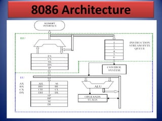
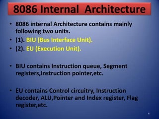
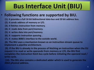
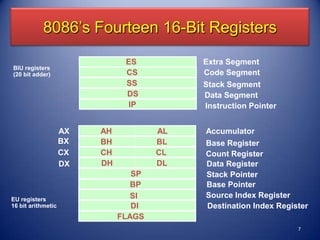
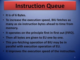
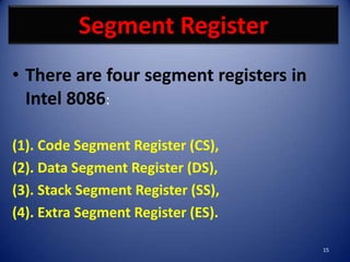
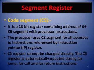
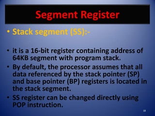
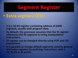
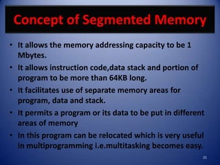
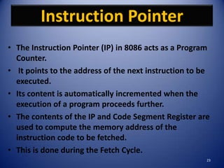
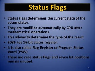
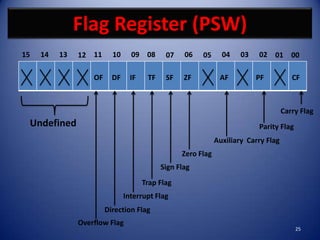
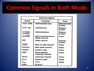
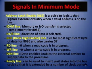
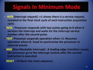
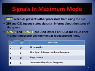
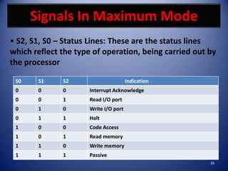
16 Bit Microprocessor
        8086


         Presented By,
     Er. Swapnil Kaware,
   svkaware@yahoo.co.in
                           1
8086 Overview
•   Introduced in 1978.
•   Having Total 40 Pins.
•   Having Address Bus of 20 bit.
•   Having Data Bus of 16 bit.
•   HMOS Microprocessor.
•   Consumes Low Power (i.e. 360 mA on 5v).
•   Clock Frequencies of 5,8 &10 MHz.
•   Contains About 29000 Transistors.
•   Can Address up to 1 Mbytes of Memory.
•   It has more than 20,000 instructions.
•   Provides fourteen 16-Bit registers.       2
8086 Architecture


                    3
8086 Internal Architecture
• 8086 internal Architecture contains mainly
  following two units.
• (1). BIU (Bus Interface Unit).
• (2). EU (Execution Unit).

• BIU contains Instruction queue, Segment
  registers,Instruction pointer,etc.

• EU contains Control circuitry, Instruction
  decoder, ALU,Pointer and Index register, Flag
  register,etc.
                                                  4
Bus Interface Unit (BIU)
• Following functions are supported by BIU.
  (1). It provides a full 16 bit bidirectional data bus and 20 bit address bus.
  (2). It sends address of memory or I/O.
  (3). It fetches instruction from memory.
  (4). It reads data from port/memory.
  (5). It writes data into port/memory.
  (6). It supports instruction queuing .
  (7). It makes 8086’s interface to the outside world.
  (8). The BIU uses a mechanism known as an instruction stream queue to
 implement a pipeline architecture.
  (9). If the BIU is already in the process of fetching an instruction when the EU
 request it to read or write operands from memory or I/O, the BIU first
 completes the instruction fetch bus cycle before initiating the operand read /
 write cycle.
  (10). The BIU also contains a dedicated adder which is used to generate the
 20bit physical address.
                                                                                  5
Execution Unit (EU)
• Following functions are supported by BIU.
 (1). The Execution unit is responsible for decoding and executing all
 instructions.
 (2). The EU extracts instructions from the top of the queue in the BIU.
 (3). During the execution of the instruction, the EU tests the status and
 control flags and updates them based on the results of executing the
 instruction.
 (4). If the queue is empty, the EU waits for the next instruction byte to
 be fetched and shifted to top of the queue.
 (5). The EU accesses the queue from the output end. It reads one
 instruction byte after the other from the output of the queue.
 (6). It tells BIU from where to fetch instructions or data,decodes
 instructions & execute instructions.                                      6
8086’s Fourteen 16-Bit Registers
                               ES          Extra Segment
BIU registers
(20 bit adder)                 CS          Code Segment
                               SS          Stack Segment
                               DS          Data Segment
                                IP         Instruction Pointer


                    AX   AH           AL   Accumulator
                    BX   BH           BL   Base Register
                    CX   CH           CL   Count Register
                    DX   DH           DL   Data Register
                                 SP        Stack Pointer
                                 BP        Base Pointer
EU registers                     SI        Source Index Register
16 bit arithmetic                DI        Destination Index Register
                              FLAGS
                                                                  7
Instruction Queue
• It is of 6 Bytes.
• To increase the execution speed, BIU fetches as
  many as six instruction bytes ahead to time from
  memory.
• It operates on the principle first in first out (FIFO).
• Then all bytes are given to EU one by one.
• This pre-fetching operation of BIU may be in
  parallel with execution operation of EU.
• It improves the execution speed of the instruction.
                                                        8
Registers of 8086

• Intel 8086 contains following registers:

•   General Purpose Registers
•   Pointer and Index Registers
•   Segment Registers
•   Instruction Pointer
•   Status Flags
                                             9
General Purpose Registers

• There are four 16-bit general purpose
  registers:

•   AX
•   BX
•   CX
•   DX

                                          10
General Purpose Registers
• Each of these 16-bit registers are further
  subdivided into two 8-bit registers.

  AX                           AH       AL
  BX                           BH       BL
  CX                           CH       CL
  DX                           DH       DL
                                               11
General Purpose Registers

• AX Register: AX register is also known as
  accumulator register that stores operands for
  arithmetic operation like divided, rotate.
• BX Register: This register is mainly used as a base
  register. It holds the starting base location of a
  memory region within a data segment.
• CX Register: It is defined as a counter. It is primarily
  used in loop instruction to store loop counter.
• DX Register: DX register is used to contain I/O port
  address for I/O instruction.
                                                       12
Pointer & Index Register
• Following four registers are under this category:

•   (1). Stack Pointer (SP),
•   (2). Base Pointer (BP),
•   (3). Source Index (SI),
•   (4). Destination Index (DI).


                                                 13
Pointer & Index Register
• Following Registers can also be used as a general Purpose
  Registers.
(1). Stack Pointer (SP) is a 16-bit register pointing to program Stack, also contains
    16-Bit offset address.

(2). Base Pointer (BP) is a 16-bit register pointing to data in stack segment. BP
    register is usually used for based indexed or register indirect addressing.

(3). Source Index (SI) is a 16-bit register. SI is used for indexed, based indexed and
    register indirect addressing, as well as a source data address in string
    manipulation Instructions

(4). Destination Index (DI) is a 16-bit register. DI is used for indexed, based
    indexed and register indirect addressing, as well as a destination data address
    in string manipulation instructions.
                                                                                    14
Segment Register
• There are four segment registers in
  Intel 8086:

(1). Code Segment Register (CS),
(2). Data Segment Register (DS),
(3). Stack Segment Register (SS),
(4). Extra Segment Register (ES).

                                        15
Segment Register
• A segment register points to the starting address of a
  memory segment.

• For e.g.:
• The code segment register points to the starting address
  of the code segment.

• The data segment register points to the starting address
  of the data segment, and so on.

• The maximum capacity of a segment may be up to 64 KB.
                                                           16
Segment Register
• Code segment (CS):-
• It is a 16-bit register containing address of 64
  KB segment with processor instructions.
• The processor uses CS segment for all accesses
  to instructions referenced by instruction
  pointer (IP) register.
• CS register cannot be changed directly. The CS
  register is automatically updated during far
  jump, far call and far return instructions
                                                 17
Segment Register
• Stack segment (SS):-

• it is a 16-bit register containing address of
  64KB segment with program stack.
• By default, the processor assumes that all
  data referenced by the stack pointer (SP)
  and base pointer (BP) registers is located in
  the stack segment.
• SS register can be changed directly using
  POP instruction.
                                             18
Segment Register
• Data segment (DS):-
• It is a 16-bit register containing address of 64KB
  segment with program data.
• By default, the processor assumes that all data
  referenced by general registers (AX, BX, CX, DX)
  and index register (SI, DI) is located in the data
  segment.
• DS register can be changed directly using POP and
  LDS instructions.
                                                   19
Segment Register
• Extra segment (ES):-

• It is a 16-bit register containing address of 64KB
  segment, usually with program data.
• By default, the processor assumes that the DI register
  references the ES segment in string manipulation
  instructions.
• ES register can be changed directly using POP and LES
  instructions.
• It is possible to change default segments used by general
  and index registers by prefixing instructions with a
  CS, SS,DS or ES prefix.
                                                          20
Concept of Segmented Memory
• It allows the memory addressing capacity to be 1
  Mbytes.
• It allows instruction code,data stack and portion of
  program to be more than 64KB long.
• It facilitates use of separate memory areas for
  program, data and stack.
• It permits a program or its data to be put in different
  areas of memory
• In this program can be relocated which is very useful
  in multiprogramming i.e.multitasking becomes easy.
                                                        21
Concept of Segmented Memory
          FFFFFH   Highest Address

          7FFFFH   Top Of Extra Segment
  64KB
                   Extra Segment Base ES=7000H

          5FFFFH   Top Of Stack Segment
  64KB
         50000H    Stack Segment Base SS=5000H

         4489FH    Top Of Code Segment
  64KB
         348A0H    Code Segment Base CS=348AH

         2FFFFH    Top Of Data Segment
  64KB
         20000H    Bottom Of Data Segment
                                                 22
Instruction Pointer
• The Instruction Pointer (IP) in 8086 acts as a Program
  Counter.
• It points to the address of the next instruction to be
  executed.
• Its content is automatically incremented when the
  execution of a program proceeds further.
• The contents of the IP and Code Segment Register are
  used to compute the memory address of the
  instruction code to be fetched.
• This is done during the Fetch Cycle.
                                                       23
Status Flags
• Status Flags determines the current state of the
  accumulator.
• They are modified automatically by CPU after
  mathematical operations.
• This allows to determine the type of the result.
• 8086 has 16-bit status register.
• It is also called Flag Register or Program Status
  Word (PSW).
• There are nine status flags and seven bit positions
  remain unused.
                                                   24
Flag Register (PSW)
15   14   13   12 11      10     09 08       07    06   05      04    03   02 01 00

                   OF     DF     IF    TF    SF    ZF          AF          PF           CF


                                                                                     Carry Flag
 Undefined                                                                 Parity Flag
                                                              Auxiliary Carry Flag
                                                  Zero Flag
                                            Sign Flag
                                      Trap Flag
                               Interrupt Flag
                        Direction Flag
               Overflow Flag
                                                                                         25
Flag Register (PSW)

• 8086 has 9 flags and they are divided into
  two categories:

• (1). Condition Flags,

• (2). Control Flags.

                                           26
Flag Register (PSW)
• Following are the nine flags:

          Condition Flags          Control Flags
   1. Carry Flag             1. Trap Flag
   2. Auxiliary Carry Flag   2. Interrupt Flag
   3. Zero Flag              3. Directional Flag
   4. Sign Flag
   5. Parity Flag
   6. Overflow Flag

                                                   27
Flag Register (PSW)
• Overflow Flag (OF): It occurs when signed numbers are added or
    subtracted. An OF indicates that the result has exceeded the capacity of machine.
• Trap Flag (TP): It is used for single step control.
•   It allows user to execute one instruction of a program at a time for debugging.
•   When trap flag is set, program can be run in single step mode.
• Interrupt Flag (IF): It is an interrupt enable / disable flag.
•   If it is set, the INTR interrupt of 8086 is enabled and if it is reset then INTR is
    disabled.
•   It can be set by executing instruction STI and can be cleared by executing CLI
    instruction.
• Direction Flag (DF): It is used in string operation.
•   If it is set, string bytes are accessed from higher memory address to lower
    memory address.
•   When it is reset, the string bytes are accessed from lower memory address to
    higher memory address.
•   It is set with STD instruction and cleared with CLDinstruction.
                                                                                          28
Pin Diagram of 8086


   8086
Pin Diagram


                            29
Function Of Pins of 8086
• AD15-AD0: These are the time multiplexed
  memory I/O address and data lines.

• A19/S6,A18/S5,A17/S4,A16/S3: These are the
  time multiplexed address and status lines.
• During T1 these are the most significant address
  lines for memory operations.
• During I/O operations, these lines are low.
• The S4 and S3 combination indicates which
  segment register is presently being used for
  memory accesses.                              30
Function Of Pins of 8086
       S4 Pin               S3 Pin                          Indication
       0                0                Alternate data
       0                1                Stack
       1                0                Code or None
       1                1                Data

BHE (Bus High Enable) /S7: The bus high enable is used to indicate the transfer of data
over the higher order ( D15-D8 ) data bus as shown in table.
      BHE Pin           A0 Pin                             Indication
      0                 0               Whole Word
      0                 1               Upper Byte from/to odd address
      1                 0               Lower Byte from/to even address
      1                 1               None                            31
Function Of Pins of 8086
• RD: This signal on low indicates the peripheral that
  the processor is performing memory or I/O read
  operation.
• READY: This is the acknowledgement from the slow
  device or memory that they have completed the
  data transfer.
• INTR-Interrupt Request: This is a triggered input. If
  any interrupt request is pending, the processor
  enters the interrupt acknowledge cycle. This can be
  internally masked by resulting the interrupt enable
  flag. This signal is active high and internally
  synchronized.                                     32
Function Of Pins of 8086
• TEST: This input is examined by a ‘WAIT’ instruction. If
  the TEST pin goes low, execution will continue, else the
  processor remains in an idle state

• CLK- Clock Input: The clock input provides the basic
  timing for processor operation and bus control activity.

• MN/MX: The logic level at this pin decides whether the
  processor is to operate in either minimum or maximum
  mode.

                                                       33
Operating Modes Of 8086
• 8086 microprocessors can be configured to work in either of
  the two modes:
• (1). Minimum Mode,
• (2). Maximum Mode.

• Minimum mode:
– Pull MN/MX to logic 1
– Typically smaller systems and contains a single microprocessor

• Maximum mode:
– Pull MN/MX logic 0
– Larger systems with more than one microprocessor.
                                                             34
Common Signals In Both Mode


                              35
Signals In Minimum Mode
- Address Latch Enable (ALE) is a pulse to logic 1 that
   signals external circuitry when a valid address is on the
   bus.
– IO/M line: Memory or I/O transfer is selected
   (complement for 8086).
– DT/R line: direction of data is selected.
– BHE (Bank High Enable) line : =0 for most significant byte
   of data for 8086 and also carries S7
– RD line: =0 when a read cycle is in progress.
– WR line: =0 when a write cycle is in progress.
– DEN line: (Data enable) Enables the external devices to
   supply data to the processor.
– Ready line: can be used to insert wait states into the bus
   cycle so that it is extended by a number of clock periods.
                                                           36
Signals In Minimum Mode
- INTR (Interrupt request) :=1 shows there is a service request,
   sampled at the final clock cycle of each instruction acquisition
   cycle.
– INTA : Processor responds with two pulses going to 0 when it
   services the interrupt and waits for the interrupt service
   number after the second pulse.
– TEST: Processor suspends operation when =1. Resumes
   operation when=0. Used to synchronize the processor to
   external events.
– NMI (Non Maskable interrupt) : A leading edge transition causes
   the processor go to the interrupt routine after the current
   instruction is executed.
– RESET : =0 Starts the reset sequence.
                                                                   37
Signals In Maximum Mode
• LOCK: when=0, prevents other processors from using the bus
• QS0 and QS1 (queue status signals) : informs about the status of
   the queue
• RQ/GT0 and RQ/GT1 are used instead of HOLD and HLDA lines
   in a multiprocessor environment as request/grant lines.

    QS 1    QS0                      Indication

    0       0       No operation

    0       1       First byte of the opcode from the queue

    1       0       Empty queue

    1       1       Subsequent byte from the queue

                                                                38
Signals In Maximum Mode
• S2, S1, S0 – Status Lines: These are the status lines
which reflect the type of operation, being carried out by
the processor

 S0    S1     S2                       Indication
 0     0      0       Interrupt Acknowledge
 0     0      1       Read I/O port
 0     1      0       Write I/O port
 0     1      1       Halt
 1     0      0       Code Access
 1     0      1       Read memory
 1     1      0       Write memory
 1     1      1       Passive
                                                       39
END OF 8086
ARCHITECTURE
SESSION
               40

8086 architecture By Er. Swapnil Kaware

  • 1.
    16 Bit Microprocessor 8086 Presented By, Er. Swapnil Kaware, svkaware@yahoo.co.in 1
  • 2.
    8086 Overview • Introduced in 1978. • Having Total 40 Pins. • Having Address Bus of 20 bit. • Having Data Bus of 16 bit. • HMOS Microprocessor. • Consumes Low Power (i.e. 360 mA on 5v). • Clock Frequencies of 5,8 &10 MHz. • Contains About 29000 Transistors. • Can Address up to 1 Mbytes of Memory. • It has more than 20,000 instructions. • Provides fourteen 16-Bit registers. 2
  • 3.
  • 4.
    8086 Internal Architecture •8086 internal Architecture contains mainly following two units. • (1). BIU (Bus Interface Unit). • (2). EU (Execution Unit). • BIU contains Instruction queue, Segment registers,Instruction pointer,etc. • EU contains Control circuitry, Instruction decoder, ALU,Pointer and Index register, Flag register,etc. 4
  • 5.
    Bus Interface Unit(BIU) • Following functions are supported by BIU. (1). It provides a full 16 bit bidirectional data bus and 20 bit address bus. (2). It sends address of memory or I/O. (3). It fetches instruction from memory. (4). It reads data from port/memory. (5). It writes data into port/memory. (6). It supports instruction queuing . (7). It makes 8086’s interface to the outside world. (8). The BIU uses a mechanism known as an instruction stream queue to implement a pipeline architecture. (9). If the BIU is already in the process of fetching an instruction when the EU request it to read or write operands from memory or I/O, the BIU first completes the instruction fetch bus cycle before initiating the operand read / write cycle. (10). The BIU also contains a dedicated adder which is used to generate the 20bit physical address. 5
  • 6.
    Execution Unit (EU) •Following functions are supported by BIU. (1). The Execution unit is responsible for decoding and executing all instructions. (2). The EU extracts instructions from the top of the queue in the BIU. (3). During the execution of the instruction, the EU tests the status and control flags and updates them based on the results of executing the instruction. (4). If the queue is empty, the EU waits for the next instruction byte to be fetched and shifted to top of the queue. (5). The EU accesses the queue from the output end. It reads one instruction byte after the other from the output of the queue. (6). It tells BIU from where to fetch instructions or data,decodes instructions & execute instructions. 6
  • 7.
    8086’s Fourteen 16-BitRegisters ES Extra Segment BIU registers (20 bit adder) CS Code Segment SS Stack Segment DS Data Segment IP Instruction Pointer AX AH AL Accumulator BX BH BL Base Register CX CH CL Count Register DX DH DL Data Register SP Stack Pointer BP Base Pointer EU registers SI Source Index Register 16 bit arithmetic DI Destination Index Register FLAGS 7
  • 8.
    Instruction Queue • Itis of 6 Bytes. • To increase the execution speed, BIU fetches as many as six instruction bytes ahead to time from memory. • It operates on the principle first in first out (FIFO). • Then all bytes are given to EU one by one. • This pre-fetching operation of BIU may be in parallel with execution operation of EU. • It improves the execution speed of the instruction. 8
  • 9.
    Registers of 8086 •Intel 8086 contains following registers: • General Purpose Registers • Pointer and Index Registers • Segment Registers • Instruction Pointer • Status Flags 9
  • 10.
    General Purpose Registers •There are four 16-bit general purpose registers: • AX • BX • CX • DX 10
  • 11.
    General Purpose Registers •Each of these 16-bit registers are further subdivided into two 8-bit registers. AX AH AL BX BH BL CX CH CL DX DH DL 11
  • 12.
    General Purpose Registers •AX Register: AX register is also known as accumulator register that stores operands for arithmetic operation like divided, rotate. • BX Register: This register is mainly used as a base register. It holds the starting base location of a memory region within a data segment. • CX Register: It is defined as a counter. It is primarily used in loop instruction to store loop counter. • DX Register: DX register is used to contain I/O port address for I/O instruction. 12
  • 13.
    Pointer & IndexRegister • Following four registers are under this category: • (1). Stack Pointer (SP), • (2). Base Pointer (BP), • (3). Source Index (SI), • (4). Destination Index (DI). 13
  • 14.
    Pointer & IndexRegister • Following Registers can also be used as a general Purpose Registers. (1). Stack Pointer (SP) is a 16-bit register pointing to program Stack, also contains 16-Bit offset address. (2). Base Pointer (BP) is a 16-bit register pointing to data in stack segment. BP register is usually used for based indexed or register indirect addressing. (3). Source Index (SI) is a 16-bit register. SI is used for indexed, based indexed and register indirect addressing, as well as a source data address in string manipulation Instructions (4). Destination Index (DI) is a 16-bit register. DI is used for indexed, based indexed and register indirect addressing, as well as a destination data address in string manipulation instructions. 14
  • 15.
    Segment Register • Thereare four segment registers in Intel 8086: (1). Code Segment Register (CS), (2). Data Segment Register (DS), (3). Stack Segment Register (SS), (4). Extra Segment Register (ES). 15
  • 16.
    Segment Register • Asegment register points to the starting address of a memory segment. • For e.g.: • The code segment register points to the starting address of the code segment. • The data segment register points to the starting address of the data segment, and so on. • The maximum capacity of a segment may be up to 64 KB. 16
  • 17.
    Segment Register • Codesegment (CS):- • It is a 16-bit register containing address of 64 KB segment with processor instructions. • The processor uses CS segment for all accesses to instructions referenced by instruction pointer (IP) register. • CS register cannot be changed directly. The CS register is automatically updated during far jump, far call and far return instructions 17
  • 18.
    Segment Register • Stacksegment (SS):- • it is a 16-bit register containing address of 64KB segment with program stack. • By default, the processor assumes that all data referenced by the stack pointer (SP) and base pointer (BP) registers is located in the stack segment. • SS register can be changed directly using POP instruction. 18
  • 19.
    Segment Register • Datasegment (DS):- • It is a 16-bit register containing address of 64KB segment with program data. • By default, the processor assumes that all data referenced by general registers (AX, BX, CX, DX) and index register (SI, DI) is located in the data segment. • DS register can be changed directly using POP and LDS instructions. 19
  • 20.
    Segment Register • Extrasegment (ES):- • It is a 16-bit register containing address of 64KB segment, usually with program data. • By default, the processor assumes that the DI register references the ES segment in string manipulation instructions. • ES register can be changed directly using POP and LES instructions. • It is possible to change default segments used by general and index registers by prefixing instructions with a CS, SS,DS or ES prefix. 20
  • 21.
    Concept of SegmentedMemory • It allows the memory addressing capacity to be 1 Mbytes. • It allows instruction code,data stack and portion of program to be more than 64KB long. • It facilitates use of separate memory areas for program, data and stack. • It permits a program or its data to be put in different areas of memory • In this program can be relocated which is very useful in multiprogramming i.e.multitasking becomes easy. 21
  • 22.
    Concept of SegmentedMemory FFFFFH Highest Address 7FFFFH Top Of Extra Segment 64KB Extra Segment Base ES=7000H 5FFFFH Top Of Stack Segment 64KB 50000H Stack Segment Base SS=5000H 4489FH Top Of Code Segment 64KB 348A0H Code Segment Base CS=348AH 2FFFFH Top Of Data Segment 64KB 20000H Bottom Of Data Segment 22
  • 23.
    Instruction Pointer • TheInstruction Pointer (IP) in 8086 acts as a Program Counter. • It points to the address of the next instruction to be executed. • Its content is automatically incremented when the execution of a program proceeds further. • The contents of the IP and Code Segment Register are used to compute the memory address of the instruction code to be fetched. • This is done during the Fetch Cycle. 23
  • 24.
    Status Flags • StatusFlags determines the current state of the accumulator. • They are modified automatically by CPU after mathematical operations. • This allows to determine the type of the result. • 8086 has 16-bit status register. • It is also called Flag Register or Program Status Word (PSW). • There are nine status flags and seven bit positions remain unused. 24
  • 25.
    Flag Register (PSW) 15 14 13 12 11 10 09 08 07 06 05 04 03 02 01 00 OF DF IF TF SF ZF AF PF CF Carry Flag Undefined Parity Flag Auxiliary Carry Flag Zero Flag Sign Flag Trap Flag Interrupt Flag Direction Flag Overflow Flag 25
  • 26.
    Flag Register (PSW) •8086 has 9 flags and they are divided into two categories: • (1). Condition Flags, • (2). Control Flags. 26
  • 27.
    Flag Register (PSW) •Following are the nine flags: Condition Flags Control Flags 1. Carry Flag 1. Trap Flag 2. Auxiliary Carry Flag 2. Interrupt Flag 3. Zero Flag 3. Directional Flag 4. Sign Flag 5. Parity Flag 6. Overflow Flag 27
  • 28.
    Flag Register (PSW) •Overflow Flag (OF): It occurs when signed numbers are added or subtracted. An OF indicates that the result has exceeded the capacity of machine. • Trap Flag (TP): It is used for single step control. • It allows user to execute one instruction of a program at a time for debugging. • When trap flag is set, program can be run in single step mode. • Interrupt Flag (IF): It is an interrupt enable / disable flag. • If it is set, the INTR interrupt of 8086 is enabled and if it is reset then INTR is disabled. • It can be set by executing instruction STI and can be cleared by executing CLI instruction. • Direction Flag (DF): It is used in string operation. • If it is set, string bytes are accessed from higher memory address to lower memory address. • When it is reset, the string bytes are accessed from lower memory address to higher memory address. • It is set with STD instruction and cleared with CLDinstruction. 28
  • 29.
    Pin Diagram of8086 8086 Pin Diagram 29
  • 30.
    Function Of Pinsof 8086 • AD15-AD0: These are the time multiplexed memory I/O address and data lines. • A19/S6,A18/S5,A17/S4,A16/S3: These are the time multiplexed address and status lines. • During T1 these are the most significant address lines for memory operations. • During I/O operations, these lines are low. • The S4 and S3 combination indicates which segment register is presently being used for memory accesses. 30
  • 31.
    Function Of Pinsof 8086 S4 Pin S3 Pin Indication 0 0 Alternate data 0 1 Stack 1 0 Code or None 1 1 Data BHE (Bus High Enable) /S7: The bus high enable is used to indicate the transfer of data over the higher order ( D15-D8 ) data bus as shown in table. BHE Pin A0 Pin Indication 0 0 Whole Word 0 1 Upper Byte from/to odd address 1 0 Lower Byte from/to even address 1 1 None 31
  • 32.
    Function Of Pinsof 8086 • RD: This signal on low indicates the peripheral that the processor is performing memory or I/O read operation. • READY: This is the acknowledgement from the slow device or memory that they have completed the data transfer. • INTR-Interrupt Request: This is a triggered input. If any interrupt request is pending, the processor enters the interrupt acknowledge cycle. This can be internally masked by resulting the interrupt enable flag. This signal is active high and internally synchronized. 32
  • 33.
    Function Of Pinsof 8086 • TEST: This input is examined by a ‘WAIT’ instruction. If the TEST pin goes low, execution will continue, else the processor remains in an idle state • CLK- Clock Input: The clock input provides the basic timing for processor operation and bus control activity. • MN/MX: The logic level at this pin decides whether the processor is to operate in either minimum or maximum mode. 33
  • 34.
    Operating Modes Of8086 • 8086 microprocessors can be configured to work in either of the two modes: • (1). Minimum Mode, • (2). Maximum Mode. • Minimum mode: – Pull MN/MX to logic 1 – Typically smaller systems and contains a single microprocessor • Maximum mode: – Pull MN/MX logic 0 – Larger systems with more than one microprocessor. 34
  • 35.
    Common Signals InBoth Mode 35
  • 36.
    Signals In MinimumMode - Address Latch Enable (ALE) is a pulse to logic 1 that signals external circuitry when a valid address is on the bus. – IO/M line: Memory or I/O transfer is selected (complement for 8086). – DT/R line: direction of data is selected. – BHE (Bank High Enable) line : =0 for most significant byte of data for 8086 and also carries S7 – RD line: =0 when a read cycle is in progress. – WR line: =0 when a write cycle is in progress. – DEN line: (Data enable) Enables the external devices to supply data to the processor. – Ready line: can be used to insert wait states into the bus cycle so that it is extended by a number of clock periods. 36
  • 37.
    Signals In MinimumMode - INTR (Interrupt request) :=1 shows there is a service request, sampled at the final clock cycle of each instruction acquisition cycle. – INTA : Processor responds with two pulses going to 0 when it services the interrupt and waits for the interrupt service number after the second pulse. – TEST: Processor suspends operation when =1. Resumes operation when=0. Used to synchronize the processor to external events. – NMI (Non Maskable interrupt) : A leading edge transition causes the processor go to the interrupt routine after the current instruction is executed. – RESET : =0 Starts the reset sequence. 37
  • 38.
    Signals In MaximumMode • LOCK: when=0, prevents other processors from using the bus • QS0 and QS1 (queue status signals) : informs about the status of the queue • RQ/GT0 and RQ/GT1 are used instead of HOLD and HLDA lines in a multiprocessor environment as request/grant lines. QS 1 QS0 Indication 0 0 No operation 0 1 First byte of the opcode from the queue 1 0 Empty queue 1 1 Subsequent byte from the queue 38
  • 39.
    Signals In MaximumMode • S2, S1, S0 – Status Lines: These are the status lines which reflect the type of operation, being carried out by the processor S0 S1 S2 Indication 0 0 0 Interrupt Acknowledge 0 0 1 Read I/O port 0 1 0 Write I/O port 0 1 1 Halt 1 0 0 Code Access 1 0 1 Read memory 1 1 0 Write memory 1 1 1 Passive 39
  • 40.