SlideShare a Scribd company logo
1 of 15
Page 1 of 15
Microprocessor & Interfacing Notes By Er. Swapnil V. Kaware (svkaware@yahoo.co.in)
Chapter No. 04. Interfacing Devices II
Q(1). Draw block diagram of 8253 PIC?.
(i). Data Bus buffer:-
The data bus buffer is bidirectional, 8-bit buffer and is used to interface the timer 8253 to the
system data bus. The operation of this buffer is controlled by the chip select line (‘CS’) which
tells the timer chip that the microprocessor is communicating with it, i.e. trying to transfer
information to or from it even though ‘CS’ is part of the READ/WRITE control logic. Data is
transmitted or received by the buffer upon execution of IN PORT or OUR PORT instruction from
CPU.
The data bus buffer has three basic functions:
(i) Programming the modes of 8253, (ii) Loading the count value in timers, (iii) Reading the
count value from timers.
The data bus buffer is connected to processor using D7-D0 pins which are bidirectional. The
data transfer takes place through these pins. These pins will be in high-impedance (or tri-state)
Page 2 of 15
Microprocessor & Interfacing Notes By Er. Swapnil V. Kaware (svkaware@yahoo.co.in)
condition until the 8253 is selected by a LOW on CS and either the read operation requested by
a LOW on the R D input or a write operation requested by the WR input going LOW.
Read/ Write Logic:
It accepts inputs for the system control bus and in turn generates the control signals for overall
device operation. It is enabled or disabled by C S so that no operation can occur to change
the function unless the device has been selected by the system logic.
CS:-
The chip select input is used to enable the communication between 8253 chip and the
microprocessor by means of data bus. A low on C S enables the data bus buffers, while a high
disables the buffer. The CS input does not have any affect on the operation of three timers once
they have been initialized. The normal configuration of a system employs some decoding logic
which actives CS line, whenever a specific set of addresses that correspond to 8253 appear
on the address bus.
RD & WR: -
The read (‘RD’) and write (‘WR’) pins control the direction of data transfer on the 8-bit bus.
When the RD input pin is low, then CPU is reading data from 8253 in the form of counter value.
When WR pin is low, then CPU is writing data to 8253 in the form of mode information
or loading initial count values to counters. The RD & WR should not both be low
simultaneously. When RD & WR signals are HIGH, the data bus buffer is disabled and no data
transfer takes place between processor and 8253.
A0 & A1:
These two input lines allow the microprocessor to specify which one of the internal register in
the 8253 is going to be used for the data transfer. Fig shows how these two lines are used to
select either the control word register or one of the 16-bit counters. For example, if
there is a, “1” on both A0 & A1, and a “0‟ on WR , then the processor is writing a control word
to the control word register. These two pins are usually connected to the address bus lines,
normally of the same name (A0 & A1).
A1 A0 RD WR CS Result
0 0 1 0 0 Write Counter 0
0 1 1 0 0 Write Counter 1
1 0 1 0 0 Write Counter 2
Page 3 of 15
Microprocessor & Interfacing Notes By Er. Swapnil V. Kaware (svkaware@yahoo.co.in)
1 1 1 0 0 Write Control Word
0 0 0 1 0 Read Counter 0
0 1 0 1 0 Read Counter 1
1 0 0 1 0 Read Counter 2
1 1 0 1 0 No operation
X X 1 1 0 No operation
X X X X 1 No operation
Control Word Register: -
The control word register is used to program the timers in different modes and control their
operations. It is selected when A0 and A1 pins are 1 & 1‟. If WR is also low, it accepts
information from the data bus buffer and stores it in control word register. The information
stored then controls the operation mode of each counter, selection of binary or BCD counting
and the loading of each counting and the loading of each count register. This register can be
written into only; no read operation of this content is available. The format will be discussed
later on.
Counters:-
Each of the timers has three pins associated with it. These are clock (CLK) input, the gate
(GATE) control input and the output (OUT).
CLK:-
This clock input pin provides 16-bit timer with the signal that causes the timer to decrement.
The maximum clock frequency input is 2.6MHz. Note that the counters operate at HIGH to LOW
transition (the negative edge) of this clock input. If the signal on this pin is generated by a fixed
frequency oscillator then the user has implemented a standard timer for getting the desired
delay.
The count value to be loaded, in this case, determines the delay produced by the
timer. If the input signal is a string of randomly occurring pulses, then it is called
implementation of a counter. In this case, these clock pulses occur whenever an event takes
place. Whenever a negative transition occurs at CLK input, the count value is decremented.
From initial and value one can count the number of times an event has taken place in an
interval.
Page 4 of 15
Microprocessor & Interfacing Notes By Er. Swapnil V. Kaware (svkaware@yahoo.co.in)
GATE:-
The gate input pin is used to initiate or enable counting. The exact effect of the gate signal
depends on which of the six modes of operation is chosen.
OUTPUT:-
The output pin provides an output from the timer. Its actual use depends on the mode of
operation of the timer. The counter can be read “on the fly” without inhibiting gate pulse or
clock input. The timers are 16-bit down counters. These timers are loaded with an initial value
before triggering. Every high to low transition at CLK input decrements the count by one. The
operation of timers can be best understood by considering the internal structure of timer.
Each timer is having three elements- input element (IE), counting element (CE) and output
element (OE).
Q(2). Draw & explain Control word format of 8253 PIC?.
Page 5 of 15
Microprocessor & Interfacing Notes By Er. Swapnil V. Kaware (svkaware@yahoo.co.in)
Q(3). Explain Various modes of operation of 8253 PIC?.
8253/54 can be operated in 6 different modes.
(i).Mode0─InterruptonTerminalCount:-
It is used to generate an interrupt to the microprocessor after a certain interval. Initially the
output is low after the mode is set. The output remains LOW after the count value is loaded
into the counter. The process of decrementing the counter continues till the terminal count is
reached, i.e., the count become zero and the output goes HIGH and will remain high until it
reloads a new count. The GATE signal is high for normal counting. When GATE goes low,
counting is terminated and the current count is latched till the GATE goes high again.
(ii).Mode1–ProgrammableOneShot:-
It can be used as a mono stable multi-vibrator. The gate input is used as a trigger input in this
mode. The output remains high until the count is loaded and a trigger is applied.
(iii).Mode2–RateGenerator:-
Page 6 of 15
Microprocessor & Interfacing Notes By Er. Swapnil V. Kaware (svkaware@yahoo.co.in)
The output is normally high after initialization. Whenever the count becomes zero, another low
pulse is generated at the output and the counter will be reloaded.
(iv).Mode3–SquareWaveGenerator:-
This mode is similar to Mode 2 except the output remains low for half of the timer period and
high for the other half of the period.
(v).Mode4−SoftwareTriggeredMode:-
In this mode, the output will remain high until the timer has counted to zero, at which point the
output will pulse low and then go high again. The count is latched when the GATE signal goes
LOW. On the terminal count, the output goes low for one clock cycle then goes HIGH. This low
pulse can be used as a strobe.
(vi). Mode5–HardwareTriggeredMode:-
Page 7 of 15
Microprocessor & Interfacing Notes By Er. Swapnil V. Kaware (svkaware@yahoo.co.in)
This mode generates a strobe in response to an externally generated signal. This mode is
similar to mode 4 except that the counting is initiated by a signal at the gate input, which
means it is hardware triggered instead of software triggered. After it is initialized, the output
goes high. When the terminal count is reached, the output goes low for one clock cycle.
Q(4). Draw and explain block diagram of 8275 CRT controller?.
Page 8 of 15
Microprocessor & Interfacing Notes By Er. Swapnil V. Kaware (svkaware@yahoo.co.in)
Q(5). Draw & explain block diagram of 8237 DMA controller?.
Direct Memory Access (DMA) is a method of allowing data to be moved from one location to
another in a computer without intervention from the central processor (CPU). It is also a fast
way of transferring data within (and sometimes between) computer. The DMA I/O technique
provides direct access to the memory while the microprocessor is temporarily disabled. The
DMA controller temporarily borrows the address bus, data bus and control bus from the
Page 9 of 15
Microprocessor & Interfacing Notes By Er. Swapnil V. Kaware (svkaware@yahoo.co.in)
microprocessor and transfers the data directly from the external devices to a series of memory
locations (and vice versa).
DMA Operation:-
Two control signals are used to request and acknowledge a direct memory access (DMA)
transfer in the microprocessor-based system. The HOLD signal as an input(to the processor) is
used to request a DMA action. The HLDA signal as an output that acknowledges the DMA action
When the processor recognizes the hold, it stops its execution and enters hold cycles.
HOLD input has higher priority than INTR or NMI. The only microprocessor pin
that has a higher priority than a HOLD is the RESET pin. HLDA becomes active to indicate that
the processor has placed its buses at high-impedance state. Direct memory accesses normally
occur between an I/O device and memory without the use of the microprocessor. A DMA read
transfers data from the memory to the I/O device.
A DMA write transfers data from an I/O device to memory. The system contains
separate memory and I/O control signals. Hence the Memory & the I/O are controlled
simultaneously. The DMA controller provides memory with its address, and the controller
signal selects the I/O device during the transfer. Data transfer speed is determined by speed of
the memory device or a DMA controller. In many cases, the DMA controller slows the speed of
the system when transfers occur.
The serial PCI (Peripheral Component Interface) Express bus transfers data at
rates exceeding DMA transfers. This in modern systems has made DMA is less important. The
8237 supplies memory & I/O with control signals and memory address information during the
DMA transfer. It is actually a special-purpose microprocessor whose job is high-speed data
transfer between memory and I/O.
Page 10 of 15
Microprocessor & Interfacing Notes By Er. Swapnil V. Kaware (svkaware@yahoo.co.in)
Q(6). Draw & explain block diagram of 8237 DMA controller?.
Q(7). Explain various operating modes of 8237 DMA controller?.
A single byte (or word) is transferred. The DMA must release and re-acquire the bus for each
additional byte. This is commonly-used by devices that cannot transfer the entire block of data
immediately. The peripheral will request the DMA each time it is ready for another transfer.
The floppy disk controller only has a one-byte buffer, so it uses this mode.
(i). Block/Demand mode:-
Once the DMA acquires the system bus, an entire block of data is transferred, up to a maximum
of 64K. If the peripheral needs additional time, it can assert the READY signal. READY should
not be used excessively, and for slow peripheral transfers, the Single Transfer Mode should be
used instead.
The difference between Block and Demand is the once a Block transfer is started, it
runs until the transfer count reaches zero. DRQ only needs to be asserted until -DACK is
asserted. Demand Mode will transfer one more bytes until DRQ is de-asserted, then when DRQ
is asserted later, the transfer resumes where it was suspended. Older hard disk controllers used
Demand Mode until CPU speeds increased to the point that it was more efficient to read the
data using the CPU.
Page 11 of 15
Microprocessor & Interfacing Notes By Er. Swapnil V. Kaware (svkaware@yahoo.co.in)
(ii). Cascade mode:-
This mechanism allows a DMA channel to request the bus, but then the attached peripheral
device is responsible for placing addressing information on the bus. This is also known as ``Bus
Mastering''. When a DMA channel in Cascade Mode receives control of the bus, the DMA does
not place addresses and I/O control signals on the bus like it normally does. Instead, the DMA
only asserts the -DACK signal for this channel.
Now it is up to the device connected to that DMA channel to provide address and
bus control signals. The peripheral has complete control over the system bus, and can do reads
and/or writes to any address below 16Meg. When the peripheral is finished with bus, it
de-asserts the DRQ line, and the DMA controller can return control to the CPU or to some other
DMA channel.
Cascade Mode can be used to chain multiple DMA controllers together, and this is
exactly what DMA Channel 4 is used for in the PC. When a peripheral requests the bus on DMA
channels 0, 1, 2 or 3, the slave DMA controller asserts HLDREQ, but this wire is actually
connected to DRQ4 on the primary DMA controller. The primary DMA controller then requests
the bus from the CPU using HLDREQ.
(iv). Autoinitialize mode:-
This mode causes the DMA to perform Byte, Block or Demand transfers, but when the DMA
transfer counter reaches zero, the counter and address is set back to where they were when the
DMA channel was originally programmed. This means that as long as the device requests
transfers, they will be granted.
It is up to the CPU to move new data into the fixed buffer ahead of where the DMA is
about to transfer it for output operations, and read new data out of the buffer behind where the
DMA is writing on input operations. This technique is frequently used on audio devices that
have small or no hardware ``sample'' buffers. There is additional CPU overhead to manage this
``circular'' buffer, but in some cases this may be the only way to eliminate the latency that
occurs when the DMA counter reaches zero and the DMA stops until it is reprogrammed.
Q(8). Internal architecture of 8086 microprocessor?. OR
Q(9). Explain various registers of 8086 microprocessor?.
8086 Microprocessor is divided into two functional units, i.e., EU (Execution Unit) and BIU (Bus
Interface Unit).
Execution Unit:- The Execution unit is responsible for decoding and executing all instructions.
The EU extracts instructions from the top of the queue in the BIU, decodes them, generates
operands if necessary, passes them to the BIU and requests it to perform the read or write bys
cycles to memory or I/O and perform the operation specified by the instruction on the
operands.
Page 12 of 15
Microprocessor & Interfacing Notes By Er. Swapnil V. Kaware (svkaware@yahoo.co.in)
During the execution of the instruction, the EU tests the status and control flags and
updates them based on the results of executing the instruction. If the queue is empty, the EU
waits for the next instruction byte to be fetched and shifted to top of the queue. When the EU
executes a branch or jump instruction, it transfers control to a location corresponding to
another set of sequential instructions. Whenever this happens, the BIU automatically resets the
queue and then begins to fetch instructions from this new location to refill the queue.
ALU:- It handles all arithmetic and logical operations, like +, −, ×, /, OR, AND, NOT operations.
Flag Register:-
Page 13 of 15
Microprocessor & Interfacing Notes By Er. Swapnil V. Kaware (svkaware@yahoo.co.in)
It is a 16-bit register that behaves like a flip-flop, i.e. it changes its status according to the result
stored in the accumulator. It has 9 flags and they are divided into 2 groups − Conditional Flags
and Control Flags.
Conditional Flags:- It represents the result of the last arithmetic or logical instruction
executed. Following is the list of conditional flags,
Carry flag − This flag indicates an overflow condition for arithmetic operations.
Auxiliary flag − When an operation is performed at ALU, it results in a carry/barrow from
lower nibble (i.e. D0 – D3) to upper nibble (i.e. D4 – D7), then this flag is set, i.e. carry given by
D3 bit to D4 is AF flag. The processor uses this flag to perform binary to BCD conversion.
Parity flag − This flag is used to indicate the parity of the result, i.e. when the lower order 8-
bits of the result contains even number of 1’s, then the Parity Flag is set. For odd number of 1’s,
the Parity Flag is reset.
Zero flag − This flag is set to 1 when the result of arithmetic or logical operation is zero else it
is set to 0.
Sign flag − This flag holds the sign of the result, i.e. when the result of the operation is negative,
then the sign flag is set to 1 else set to 0.
Overflow flag − This flag represents the result when the system capacity is exceeded.
Control Flags:- Control flags controls the operations of the execution unit. Following is the list
of control flags,
Trap flag − It is used for single step control and allows the user to execute one instruction at a
time for debugging. If it is set, then the program can be run in a single step mode.
Interrupt flag − It is an interrupt enable/disable flag, i.e. used to allow/prohibit the
interruption of a program. It is set to 1 for interrupt enabled condition and set to 0 for
interrupt disabled condition.
Direction flag − It is used in string operation. As the name suggests when it is set then string
bytes are accessed from the higher memory address to the lower memory address and vice-a-
versa.
Page 14 of 15
Microprocessor & Interfacing Notes By Er. Swapnil V. Kaware (svkaware@yahoo.co.in)
General purpose register:- There are 8 general purpose registers, i.e., AH, AL, BH, BL, CH, CL,
DH, and DL. These registers can be used individually to store 8-bit data and can be used in
pairs to store 16bit data. The valid register pairs are AH and AL, BH and BL, CH and CL, and DH
and DL. It is referred to the AX, BX, CX, and DX respectively.
AX register − It is also known as accumulator register. It is used to store operands for
arithmetic operations.
BX register − It is used as a base register. It is used to store the starting base address of the
memory area within the data segment.
CX register − It is referred to as counter. It is used in loop instruction to store the loop counter.
DX register − This register is used to hold I/O port address for I/O instruction.
Stack pointer register:- It is a 16-bit register, which holds the address from the start of the
segment to the memory location, where a word was most recently stored on the stack.
BIU(BusInterfaceUnit):- The Bus Interface Unit contains Bus Interface Logic, Segment
registers, Memory addressing logic and a Six byte instruction object code queue. The BIU sends
out address, fetches the instructions from memory, read data from ports and memory, and
writes the data to ports and memory.
BIU takes care of all data and addresses transfers on the buses for the EU like
sending addresses, fetching instructions from the memory, reading data from the ports and the
memory as well as writing data to the ports and the memory. EU has no direction connection
with System Buses so this is possible with the BIU. EU and BIU are connected with the Internal
Bus. It has the following functional parts,
Instruction queue − BIU contains the instruction queue. BIU gets up to 6 bytes of next
instructions and stores them in the instruction queue. When EU executes instructions and is
ready for its next instruction, then it simply reads the instruction from this instruction queue
resulting in increased execution speed. Fetching the next instruction while the current
instruction executes is called pipelining.
Segment register − BIU has 4 segment buses, i.e. CS, DS, SS & ES. It holds the addresses of
instructions and data in memory, which are used by the processor to access memory locations.
It also contains 1 pointer register IP, which holds the address of the next instruction to
executed by the EU.
Page 15 of 15
Microprocessor & Interfacing Notes By Er. Swapnil V. Kaware (svkaware@yahoo.co.in)
CS − It stands for Code Segment. It is used for addressing a memory location in the code
segment of the memory, where the executable program is stored.
DS − It stands for Data Segment. It consists of data used by the program andis accessed in the
data segment by an offset address or the content of other register that holds the offset address.
SS − It stands for Stack Segment. It handles memory to store data and addresses during
execution.
ES − It stands for Extra Segment. ES is additional data segment, which is used by the string to
hold the extra destination data.
Instruction pointer − It is a 16-bit register used to hold the address of the next instruction to
be executed.
***************************************** ALL THE BEST *****************************************

More Related Content

What's hot

Basics of peripheral devices and Working
Basics of peripheral devices and WorkingBasics of peripheral devices and Working
Basics of peripheral devices and WorkingDr.YNM
 
DMA controller intel 8257
DMA controller intel 8257DMA controller intel 8257
DMA controller intel 8257Daniel Ilunga
 
advancsed microprocessor and interfacing
advancsed microprocessor and interfacingadvancsed microprocessor and interfacing
advancsed microprocessor and interfacing@zenafaris91
 
Pin diagram of 8085
Pin diagram of 8085Pin diagram of 8085
Pin diagram of 8085ShivamSood22
 
Architecture of 8085
Architecture of 8085Architecture of 8085
Architecture of 8085ShivamSood22
 
8259 Programmable Interrupt Controller
8259 Programmable Interrupt Controller8259 Programmable Interrupt Controller
8259 Programmable Interrupt Controllerabhikalmegh
 
8085 microprocessor Architecture and Pin description
8085 microprocessor Architecture and Pin description 8085 microprocessor Architecture and Pin description
8085 microprocessor Architecture and Pin description Vijay Kumar
 
Interfacing of data converters & io devices
Interfacing of data converters & io devicesInterfacing of data converters & io devices
Interfacing of data converters & io devicesDr.YNM
 
I/o and memory interfacing
I/o and memory interfacingI/o and memory interfacing
I/o and memory interfacingRuchi Srivastava
 

What's hot (19)

Basics of peripheral devices and Working
Basics of peripheral devices and WorkingBasics of peripheral devices and Working
Basics of peripheral devices and Working
 
DMA controller intel 8257
DMA controller intel 8257DMA controller intel 8257
DMA controller intel 8257
 
Timing diagram 8085 microprocessor
Timing diagram 8085 microprocessorTiming diagram 8085 microprocessor
Timing diagram 8085 microprocessor
 
1.ppi 8255
1.ppi 8255 1.ppi 8255
1.ppi 8255
 
Viva
VivaViva
Viva
 
Lect 5
Lect 5Lect 5
Lect 5
 
advancsed microprocessor and interfacing
advancsed microprocessor and interfacingadvancsed microprocessor and interfacing
advancsed microprocessor and interfacing
 
8085 intro
8085 intro8085 intro
8085 intro
 
Pin diagram of 8085
Pin diagram of 8085Pin diagram of 8085
Pin diagram of 8085
 
8085 instruction-set part 1
8085 instruction-set part 18085 instruction-set part 1
8085 instruction-set part 1
 
8085 microprocessor
8085 microprocessor8085 microprocessor
8085 microprocessor
 
8251 USART
8251 USART8251 USART
8251 USART
 
Architecture of 8085
Architecture of 8085Architecture of 8085
Architecture of 8085
 
8259 Programmable Interrupt Controller
8259 Programmable Interrupt Controller8259 Programmable Interrupt Controller
8259 Programmable Interrupt Controller
 
Mp 8085
Mp 8085Mp 8085
Mp 8085
 
8085
80858085
8085
 
8085 microprocessor Architecture and Pin description
8085 microprocessor Architecture and Pin description 8085 microprocessor Architecture and Pin description
8085 microprocessor Architecture and Pin description
 
Interfacing of data converters & io devices
Interfacing of data converters & io devicesInterfacing of data converters & io devices
Interfacing of data converters & io devices
 
I/o and memory interfacing
I/o and memory interfacingI/o and memory interfacing
I/o and memory interfacing
 

Viewers also liked

Introduction to-microprocessors
Introduction to-microprocessorsIntroduction to-microprocessors
Introduction to-microprocessorsVolodymyr Ushenko
 
Microprocessor and Interfacing Notes
Microprocessor and Interfacing NotesMicroprocessor and Interfacing Notes
Microprocessor and Interfacing NotesAkshansh Chaudhary
 
Microprocessor and-interfacing-techbymak
Microprocessor and-interfacing-techbymakMicroprocessor and-interfacing-techbymak
Microprocessor and-interfacing-techbymakAkshay Makadiya
 
Microprocessor Architecture
Microprocessor ArchitectureMicroprocessor Architecture
Microprocessor ArchitectureAvijeet Negel
 
Microprocessor & Assembly language by team blackhole
Microprocessor & Assembly language by team blackholeMicroprocessor & Assembly language by team blackhole
Microprocessor & Assembly language by team blackholeMd Abdus Sobur Sikdar
 
Microprocessor chapter 9 - assembly language programming
Microprocessor  chapter 9 - assembly language programmingMicroprocessor  chapter 9 - assembly language programming
Microprocessor chapter 9 - assembly language programmingWondeson Emeye
 

Viewers also liked (8)

Introduction to-microprocessors
Introduction to-microprocessorsIntroduction to-microprocessors
Introduction to-microprocessors
 
Microprocessor and Interfacing Notes
Microprocessor and Interfacing NotesMicroprocessor and Interfacing Notes
Microprocessor and Interfacing Notes
 
Lecture 1
Lecture 1Lecture 1
Lecture 1
 
Microprocessor and-interfacing-techbymak
Microprocessor and-interfacing-techbymakMicroprocessor and-interfacing-techbymak
Microprocessor and-interfacing-techbymak
 
Microprocessor Architecture
Microprocessor ArchitectureMicroprocessor Architecture
Microprocessor Architecture
 
Microprocessor & Assembly language by team blackhole
Microprocessor & Assembly language by team blackholeMicroprocessor & Assembly language by team blackhole
Microprocessor & Assembly language by team blackhole
 
Mpmc lab
Mpmc labMpmc lab
Mpmc lab
 
Microprocessor chapter 9 - assembly language programming
Microprocessor  chapter 9 - assembly language programmingMicroprocessor  chapter 9 - assembly language programming
Microprocessor chapter 9 - assembly language programming
 

Similar to Microprocessor & Interfacing (Part-2) By Er. Swapnil V. Kaware

8255-PPI MPMC text book for engineering.ppt
8255-PPI MPMC text book for engineering.ppt8255-PPI MPMC text book for engineering.ppt
8255-PPI MPMC text book for engineering.pptkhushiduppala
 
unit 2 lect 6 AND 7 8254.pptx
unit 2 lect 6 AND 7 8254.pptxunit 2 lect 6 AND 7 8254.pptx
unit 2 lect 6 AND 7 8254.pptxDrVikasMahor
 
5.programmable interval timer 8253
5.programmable interval timer 82535.programmable interval timer 8253
5.programmable interval timer 8253MdFazleRabbi18
 
8259 programmable PPI interfacing with 8085 .ppt
8259 programmable PPI interfacing with 8085 .ppt8259 programmable PPI interfacing with 8085 .ppt
8259 programmable PPI interfacing with 8085 .pptDrVikasMahor
 
Microprocessor Basics 8085 Ch-1
Microprocessor Basics 8085 Ch-1Microprocessor Basics 8085 Ch-1
Microprocessor Basics 8085 Ch-1Neelam Kapoor
 
8251 usart programmable communication interface by aniket bhute
8251  usart  programmable communication interface by aniket bhute8251  usart  programmable communication interface by aniket bhute
8251 usart programmable communication interface by aniket bhuteAniket Bhute
 
MicroProcessors and MicroControllersUnit3
MicroProcessors and MicroControllersUnit3MicroProcessors and MicroControllersUnit3
MicroProcessors and MicroControllersUnit3deepakdmaat
 
INTERFACING WITH INTEL 8251A (USART)
INTERFACING WITH INTEL 8251A (USART)INTERFACING WITH INTEL 8251A (USART)
INTERFACING WITH INTEL 8251A (USART)Prof Ansari
 
8251 a usart programmable communication interface(1)
8251 a usart   programmable communication interface(1)8251 a usart   programmable communication interface(1)
8251 a usart programmable communication interface(1)divyangpit
 
Microprocessor and microcontroller
Microprocessor and microcontrollerMicroprocessor and microcontroller
Microprocessor and microcontrollerRavinder Singla
 
IC 8253 - Microprocessor
IC 8253 - Microprocessor IC 8253 - Microprocessor
IC 8253 - Microprocessor Vatsal N Shah
 
8251 communication interface
8251 communication interface8251 communication interface
8251 communication interfaceLingalaSowjanya
 
Embedded systems and robotics by scmandota
Embedded systems and robotics by scmandotaEmbedded systems and robotics by scmandota
Embedded systems and robotics by scmandotascmandota
 
Module 3 special purpose programmable devices and their interfacing
Module 3 special purpose programmable devices and their interfacingModule 3 special purpose programmable devices and their interfacing
Module 3 special purpose programmable devices and their interfacingDeepak John
 
INTERFACING WITH INTEL 8251A (USART)
INTERFACING WITH INTEL 8251A (USART)INTERFACING WITH INTEL 8251A (USART)
INTERFACING WITH INTEL 8251A (USART)Prof Ansari
 

Similar to Microprocessor & Interfacing (Part-2) By Er. Swapnil V. Kaware (20)

8255-PPI MPMC text book for engineering.ppt
8255-PPI MPMC text book for engineering.ppt8255-PPI MPMC text book for engineering.ppt
8255-PPI MPMC text book for engineering.ppt
 
unit 2 lect 6 AND 7 8254.pptx
unit 2 lect 6 AND 7 8254.pptxunit 2 lect 6 AND 7 8254.pptx
unit 2 lect 6 AND 7 8254.pptx
 
Assembler4
Assembler4Assembler4
Assembler4
 
5.programmable interval timer 8253
5.programmable interval timer 82535.programmable interval timer 8253
5.programmable interval timer 8253
 
8259 programmable PPI interfacing with 8085 .ppt
8259 programmable PPI interfacing with 8085 .ppt8259 programmable PPI interfacing with 8085 .ppt
8259 programmable PPI interfacing with 8085 .ppt
 
Microprocessor Basics 8085 Ch-1
Microprocessor Basics 8085 Ch-1Microprocessor Basics 8085 Ch-1
Microprocessor Basics 8085 Ch-1
 
8251 usart programmable communication interface by aniket bhute
8251  usart  programmable communication interface by aniket bhute8251  usart  programmable communication interface by aniket bhute
8251 usart programmable communication interface by aniket bhute
 
MicroProcessors and MicroControllersUnit3
MicroProcessors and MicroControllersUnit3MicroProcessors and MicroControllersUnit3
MicroProcessors and MicroControllersUnit3
 
INTERFACING WITH INTEL 8251A (USART)
INTERFACING WITH INTEL 8251A (USART)INTERFACING WITH INTEL 8251A (USART)
INTERFACING WITH INTEL 8251A (USART)
 
8251 a usart programmable communication interface(1)
8251 a usart   programmable communication interface(1)8251 a usart   programmable communication interface(1)
8251 a usart programmable communication interface(1)
 
Microprocessor and microcontroller
Microprocessor and microcontrollerMicroprocessor and microcontroller
Microprocessor and microcontroller
 
8259 a
8259 a8259 a
8259 a
 
IC 8253 - Microprocessor
IC 8253 - Microprocessor IC 8253 - Microprocessor
IC 8253 - Microprocessor
 
8251 communication interface
8251 communication interface8251 communication interface
8251 communication interface
 
Peripheral 8245,16550&8237 dma controller
Peripheral 8245,16550&8237 dma controllerPeripheral 8245,16550&8237 dma controller
Peripheral 8245,16550&8237 dma controller
 
8085 (1)
8085 (1)8085 (1)
8085 (1)
 
Embedded systems and robotics by scmandota
Embedded systems and robotics by scmandotaEmbedded systems and robotics by scmandota
Embedded systems and robotics by scmandota
 
Module 3 special purpose programmable devices and their interfacing
Module 3 special purpose programmable devices and their interfacingModule 3 special purpose programmable devices and their interfacing
Module 3 special purpose programmable devices and their interfacing
 
INTERFACING WITH INTEL 8251A (USART)
INTERFACING WITH INTEL 8251A (USART)INTERFACING WITH INTEL 8251A (USART)
INTERFACING WITH INTEL 8251A (USART)
 
8253
82538253
8253
 

More from Prof. Swapnil V. Kaware

Corona Virus Awareness by, Er. Swapnil V. Kaware
Corona Virus Awareness by, Er. Swapnil V. KawareCorona Virus Awareness by, Er. Swapnil V. Kaware
Corona Virus Awareness by, Er. Swapnil V. KawareProf. Swapnil V. Kaware
 
Basic Electronics By, Er. Swapnil V. Kawrare
Basic Electronics By, Er. Swapnil V. KawrareBasic Electronics By, Er. Swapnil V. Kawrare
Basic Electronics By, Er. Swapnil V. KawrareProf. Swapnil V. Kaware
 
Addressing modes of 8085 by Er. Swapnil V. Kaware
Addressing modes of 8085 by Er. Swapnil V. KawareAddressing modes of 8085 by Er. Swapnil V. Kaware
Addressing modes of 8085 by Er. Swapnil V. KawareProf. Swapnil V. Kaware
 
Best Interview Tips By, Er. Swapnil V. Kaware
Best Interview Tips By, Er. Swapnil V. KawareBest Interview Tips By, Er. Swapnil V. Kaware
Best Interview Tips By, Er. Swapnil V. KawareProf. Swapnil V. Kaware
 
LED Lighting for Energy Efficiency By, Er. Swapnil V. Kaware
LED Lighting for Energy Efficiency By, Er. Swapnil V. KawareLED Lighting for Energy Efficiency By, Er. Swapnil V. Kaware
LED Lighting for Energy Efficiency By, Er. Swapnil V. KawareProf. Swapnil V. Kaware
 
Microprocessor Lab Manual by Er. Swapnil V. Kaware
Microprocessor Lab Manual by Er. Swapnil V. KawareMicroprocessor Lab Manual by Er. Swapnil V. Kaware
Microprocessor Lab Manual by Er. Swapnil V. KawareProf. Swapnil V. Kaware
 
Electronics Lab Manual by Er. Swapnil V. Kaware
Electronics Lab Manual by Er. Swapnil V. KawareElectronics Lab Manual by Er. Swapnil V. Kaware
Electronics Lab Manual by Er. Swapnil V. KawareProf. Swapnil V. Kaware
 
Transistors & Oscillators by Er. Swapnil Kaware
Transistors & Oscillators by Er. Swapnil KawareTransistors & Oscillators by Er. Swapnil Kaware
Transistors & Oscillators by Er. Swapnil KawareProf. Swapnil V. Kaware
 
Basic Electronics (Rectifiers) by Er. Swapnil Kaware
Basic Electronics (Rectifiers) by Er. Swapnil KawareBasic Electronics (Rectifiers) by Er. Swapnil Kaware
Basic Electronics (Rectifiers) by Er. Swapnil KawareProf. Swapnil V. Kaware
 
Digital Electronics Basics by Er. Swapnil Kaware
Digital Electronics Basics by Er. Swapnil KawareDigital Electronics Basics by Er. Swapnil Kaware
Digital Electronics Basics by Er. Swapnil KawareProf. Swapnil V. Kaware
 
Digital computer Basics by, Er. Swapnil Kaware
Digital computer Basics by, Er. Swapnil KawareDigital computer Basics by, Er. Swapnil Kaware
Digital computer Basics by, Er. Swapnil KawareProf. Swapnil V. Kaware
 
Cryptography & Network Security By, Er. Swapnil Kaware
Cryptography & Network Security By, Er. Swapnil KawareCryptography & Network Security By, Er. Swapnil Kaware
Cryptography & Network Security By, Er. Swapnil KawareProf. Swapnil V. Kaware
 
Digital signal processing By Er. Swapnil Kaware
Digital signal processing By Er. Swapnil KawareDigital signal processing By Er. Swapnil Kaware
Digital signal processing By Er. Swapnil KawareProf. Swapnil V. Kaware
 
Advanced optical communication By Er. Swapnl Kaware
Advanced optical communication By Er. Swapnl KawareAdvanced optical communication By Er. Swapnl Kaware
Advanced optical communication By Er. Swapnl KawareProf. Swapnil V. Kaware
 

More from Prof. Swapnil V. Kaware (20)

Corona Virus Awareness by, Er. Swapnil V. Kaware
Corona Virus Awareness by, Er. Swapnil V. KawareCorona Virus Awareness by, Er. Swapnil V. Kaware
Corona Virus Awareness by, Er. Swapnil V. Kaware
 
Basic Electronics By, Er. Swapnil V. Kawrare
Basic Electronics By, Er. Swapnil V. KawrareBasic Electronics By, Er. Swapnil V. Kawrare
Basic Electronics By, Er. Swapnil V. Kawrare
 
Addressing modes of 8085 by Er. Swapnil V. Kaware
Addressing modes of 8085 by Er. Swapnil V. KawareAddressing modes of 8085 by Er. Swapnil V. Kaware
Addressing modes of 8085 by Er. Swapnil V. Kaware
 
Best GD tips by, Er. Swapnil V. Kaware
Best GD tips by, Er. Swapnil V. KawareBest GD tips by, Er. Swapnil V. Kaware
Best GD tips by, Er. Swapnil V. Kaware
 
Best Interview Tips By, Er. Swapnil V. Kaware
Best Interview Tips By, Er. Swapnil V. KawareBest Interview Tips By, Er. Swapnil V. Kaware
Best Interview Tips By, Er. Swapnil V. Kaware
 
Chandrayaan 2 By, Er. Swapnil V. Kaware
Chandrayaan 2 By, Er. Swapnil V. KawareChandrayaan 2 By, Er. Swapnil V. Kaware
Chandrayaan 2 By, Er. Swapnil V. Kaware
 
LED Lighting for Energy Efficiency By, Er. Swapnil V. Kaware
LED Lighting for Energy Efficiency By, Er. Swapnil V. KawareLED Lighting for Energy Efficiency By, Er. Swapnil V. Kaware
LED Lighting for Energy Efficiency By, Er. Swapnil V. Kaware
 
Combinational Logic Circuits
Combinational Logic CircuitsCombinational Logic Circuits
Combinational Logic Circuits
 
Microprocessor Lab Manual by Er. Swapnil V. Kaware
Microprocessor Lab Manual by Er. Swapnil V. KawareMicroprocessor Lab Manual by Er. Swapnil V. Kaware
Microprocessor Lab Manual by Er. Swapnil V. Kaware
 
LED basics by Er. Swapnil V. Kaware
LED basics by Er. Swapnil V. KawareLED basics by Er. Swapnil V. Kaware
LED basics by Er. Swapnil V. Kaware
 
Electronics Lab Manual by Er. Swapnil V. Kaware
Electronics Lab Manual by Er. Swapnil V. KawareElectronics Lab Manual by Er. Swapnil V. Kaware
Electronics Lab Manual by Er. Swapnil V. Kaware
 
Transistors & Oscillators by Er. Swapnil Kaware
Transistors & Oscillators by Er. Swapnil KawareTransistors & Oscillators by Er. Swapnil Kaware
Transistors & Oscillators by Er. Swapnil Kaware
 
Basic Electronics (Rectifiers) by Er. Swapnil Kaware
Basic Electronics (Rectifiers) by Er. Swapnil KawareBasic Electronics (Rectifiers) by Er. Swapnil Kaware
Basic Electronics (Rectifiers) by Er. Swapnil Kaware
 
Basic Electronics by Er. Swapnil Kaware
Basic Electronics by Er. Swapnil KawareBasic Electronics by Er. Swapnil Kaware
Basic Electronics by Er. Swapnil Kaware
 
Digital Electronics Basics by Er. Swapnil Kaware
Digital Electronics Basics by Er. Swapnil KawareDigital Electronics Basics by Er. Swapnil Kaware
Digital Electronics Basics by Er. Swapnil Kaware
 
Digital computer Basics by, Er. Swapnil Kaware
Digital computer Basics by, Er. Swapnil KawareDigital computer Basics by, Er. Swapnil Kaware
Digital computer Basics by, Er. Swapnil Kaware
 
Cryptography & Network Security By, Er. Swapnil Kaware
Cryptography & Network Security By, Er. Swapnil KawareCryptography & Network Security By, Er. Swapnil Kaware
Cryptography & Network Security By, Er. Swapnil Kaware
 
Digital signal processing By Er. Swapnil Kaware
Digital signal processing By Er. Swapnil KawareDigital signal processing By Er. Swapnil Kaware
Digital signal processing By Er. Swapnil Kaware
 
Advanced optical communication By Er. Swapnl Kaware
Advanced optical communication By Er. Swapnl KawareAdvanced optical communication By Er. Swapnl Kaware
Advanced optical communication By Er. Swapnl Kaware
 
Digital Communication Techniques
Digital Communication TechniquesDigital Communication Techniques
Digital Communication Techniques
 

Recently uploaded

APPLICATIONS-AC/DC DRIVES-OPERATING CHARACTERISTICS
APPLICATIONS-AC/DC DRIVES-OPERATING CHARACTERISTICSAPPLICATIONS-AC/DC DRIVES-OPERATING CHARACTERISTICS
APPLICATIONS-AC/DC DRIVES-OPERATING CHARACTERISTICSKurinjimalarL3
 
VIP Call Girls Service Hitech City Hyderabad Call +91-8250192130
VIP Call Girls Service Hitech City Hyderabad Call +91-8250192130VIP Call Girls Service Hitech City Hyderabad Call +91-8250192130
VIP Call Girls Service Hitech City Hyderabad Call +91-8250192130Suhani Kapoor
 
High Profile Call Girls Nagpur Meera Call 7001035870 Meet With Nagpur Escorts
High Profile Call Girls Nagpur Meera Call 7001035870 Meet With Nagpur EscortsHigh Profile Call Girls Nagpur Meera Call 7001035870 Meet With Nagpur Escorts
High Profile Call Girls Nagpur Meera Call 7001035870 Meet With Nagpur EscortsCall Girls in Nagpur High Profile
 
College Call Girls Nashik Nehal 7001305949 Independent Escort Service Nashik
College Call Girls Nashik Nehal 7001305949 Independent Escort Service NashikCollege Call Girls Nashik Nehal 7001305949 Independent Escort Service Nashik
College Call Girls Nashik Nehal 7001305949 Independent Escort Service NashikCall Girls in Nagpur High Profile
 
MANUFACTURING PROCESS-II UNIT-2 LATHE MACHINE
MANUFACTURING PROCESS-II UNIT-2 LATHE MACHINEMANUFACTURING PROCESS-II UNIT-2 LATHE MACHINE
MANUFACTURING PROCESS-II UNIT-2 LATHE MACHINESIVASHANKAR N
 
MANUFACTURING PROCESS-II UNIT-5 NC MACHINE TOOLS
MANUFACTURING PROCESS-II UNIT-5 NC MACHINE TOOLSMANUFACTURING PROCESS-II UNIT-5 NC MACHINE TOOLS
MANUFACTURING PROCESS-II UNIT-5 NC MACHINE TOOLSSIVASHANKAR N
 
Introduction and different types of Ethernet.pptx
Introduction and different types of Ethernet.pptxIntroduction and different types of Ethernet.pptx
Introduction and different types of Ethernet.pptxupamatechverse
 
SPICE PARK APR2024 ( 6,793 SPICE Models )
SPICE PARK APR2024 ( 6,793 SPICE Models )SPICE PARK APR2024 ( 6,793 SPICE Models )
SPICE PARK APR2024 ( 6,793 SPICE Models )Tsuyoshi Horigome
 
Model Call Girl in Narela Delhi reach out to us at 🔝8264348440🔝
Model Call Girl in Narela Delhi reach out to us at 🔝8264348440🔝Model Call Girl in Narela Delhi reach out to us at 🔝8264348440🔝
Model Call Girl in Narela Delhi reach out to us at 🔝8264348440🔝soniya singh
 
Coefficient of Thermal Expansion and their Importance.pptx
Coefficient of Thermal Expansion and their Importance.pptxCoefficient of Thermal Expansion and their Importance.pptx
Coefficient of Thermal Expansion and their Importance.pptxAsutosh Ranjan
 
What are the advantages and disadvantages of membrane structures.pptx
What are the advantages and disadvantages of membrane structures.pptxWhat are the advantages and disadvantages of membrane structures.pptx
What are the advantages and disadvantages of membrane structures.pptxwendy cai
 
(MEERA) Dapodi Call Girls Just Call 7001035870 [ Cash on Delivery ] Pune Escorts
(MEERA) Dapodi Call Girls Just Call 7001035870 [ Cash on Delivery ] Pune Escorts(MEERA) Dapodi Call Girls Just Call 7001035870 [ Cash on Delivery ] Pune Escorts
(MEERA) Dapodi Call Girls Just Call 7001035870 [ Cash on Delivery ] Pune Escortsranjana rawat
 
VIP Call Girls Service Kondapur Hyderabad Call +91-8250192130
VIP Call Girls Service Kondapur Hyderabad Call +91-8250192130VIP Call Girls Service Kondapur Hyderabad Call +91-8250192130
VIP Call Girls Service Kondapur Hyderabad Call +91-8250192130Suhani Kapoor
 
Call Girls in Nagpur Suman Call 7001035870 Meet With Nagpur Escorts
Call Girls in Nagpur Suman Call 7001035870 Meet With Nagpur EscortsCall Girls in Nagpur Suman Call 7001035870 Meet With Nagpur Escorts
Call Girls in Nagpur Suman Call 7001035870 Meet With Nagpur EscortsCall Girls in Nagpur High Profile
 
the ladakh protest in leh ladakh 2024 sonam wangchuk.pptx
the ladakh protest in leh ladakh 2024 sonam wangchuk.pptxthe ladakh protest in leh ladakh 2024 sonam wangchuk.pptx
the ladakh protest in leh ladakh 2024 sonam wangchuk.pptxhumanexperienceaaa
 

Recently uploaded (20)

APPLICATIONS-AC/DC DRIVES-OPERATING CHARACTERISTICS
APPLICATIONS-AC/DC DRIVES-OPERATING CHARACTERISTICSAPPLICATIONS-AC/DC DRIVES-OPERATING CHARACTERISTICS
APPLICATIONS-AC/DC DRIVES-OPERATING CHARACTERISTICS
 
VIP Call Girls Service Hitech City Hyderabad Call +91-8250192130
VIP Call Girls Service Hitech City Hyderabad Call +91-8250192130VIP Call Girls Service Hitech City Hyderabad Call +91-8250192130
VIP Call Girls Service Hitech City Hyderabad Call +91-8250192130
 
★ CALL US 9953330565 ( HOT Young Call Girls In Badarpur delhi NCR
★ CALL US 9953330565 ( HOT Young Call Girls In Badarpur delhi NCR★ CALL US 9953330565 ( HOT Young Call Girls In Badarpur delhi NCR
★ CALL US 9953330565 ( HOT Young Call Girls In Badarpur delhi NCR
 
High Profile Call Girls Nagpur Meera Call 7001035870 Meet With Nagpur Escorts
High Profile Call Girls Nagpur Meera Call 7001035870 Meet With Nagpur EscortsHigh Profile Call Girls Nagpur Meera Call 7001035870 Meet With Nagpur Escorts
High Profile Call Girls Nagpur Meera Call 7001035870 Meet With Nagpur Escorts
 
College Call Girls Nashik Nehal 7001305949 Independent Escort Service Nashik
College Call Girls Nashik Nehal 7001305949 Independent Escort Service NashikCollege Call Girls Nashik Nehal 7001305949 Independent Escort Service Nashik
College Call Girls Nashik Nehal 7001305949 Independent Escort Service Nashik
 
MANUFACTURING PROCESS-II UNIT-2 LATHE MACHINE
MANUFACTURING PROCESS-II UNIT-2 LATHE MACHINEMANUFACTURING PROCESS-II UNIT-2 LATHE MACHINE
MANUFACTURING PROCESS-II UNIT-2 LATHE MACHINE
 
MANUFACTURING PROCESS-II UNIT-5 NC MACHINE TOOLS
MANUFACTURING PROCESS-II UNIT-5 NC MACHINE TOOLSMANUFACTURING PROCESS-II UNIT-5 NC MACHINE TOOLS
MANUFACTURING PROCESS-II UNIT-5 NC MACHINE TOOLS
 
Introduction and different types of Ethernet.pptx
Introduction and different types of Ethernet.pptxIntroduction and different types of Ethernet.pptx
Introduction and different types of Ethernet.pptx
 
9953056974 Call Girls In South Ex, Escorts (Delhi) NCR.pdf
9953056974 Call Girls In South Ex, Escorts (Delhi) NCR.pdf9953056974 Call Girls In South Ex, Escorts (Delhi) NCR.pdf
9953056974 Call Girls In South Ex, Escorts (Delhi) NCR.pdf
 
SPICE PARK APR2024 ( 6,793 SPICE Models )
SPICE PARK APR2024 ( 6,793 SPICE Models )SPICE PARK APR2024 ( 6,793 SPICE Models )
SPICE PARK APR2024 ( 6,793 SPICE Models )
 
Model Call Girl in Narela Delhi reach out to us at 🔝8264348440🔝
Model Call Girl in Narela Delhi reach out to us at 🔝8264348440🔝Model Call Girl in Narela Delhi reach out to us at 🔝8264348440🔝
Model Call Girl in Narela Delhi reach out to us at 🔝8264348440🔝
 
Coefficient of Thermal Expansion and their Importance.pptx
Coefficient of Thermal Expansion and their Importance.pptxCoefficient of Thermal Expansion and their Importance.pptx
Coefficient of Thermal Expansion and their Importance.pptx
 
What are the advantages and disadvantages of membrane structures.pptx
What are the advantages and disadvantages of membrane structures.pptxWhat are the advantages and disadvantages of membrane structures.pptx
What are the advantages and disadvantages of membrane structures.pptx
 
Call Us -/9953056974- Call Girls In Vikaspuri-/- Delhi NCR
Call Us -/9953056974- Call Girls In Vikaspuri-/- Delhi NCRCall Us -/9953056974- Call Girls In Vikaspuri-/- Delhi NCR
Call Us -/9953056974- Call Girls In Vikaspuri-/- Delhi NCR
 
Exploring_Network_Security_with_JA3_by_Rakesh Seal.pptx
Exploring_Network_Security_with_JA3_by_Rakesh Seal.pptxExploring_Network_Security_with_JA3_by_Rakesh Seal.pptx
Exploring_Network_Security_with_JA3_by_Rakesh Seal.pptx
 
(MEERA) Dapodi Call Girls Just Call 7001035870 [ Cash on Delivery ] Pune Escorts
(MEERA) Dapodi Call Girls Just Call 7001035870 [ Cash on Delivery ] Pune Escorts(MEERA) Dapodi Call Girls Just Call 7001035870 [ Cash on Delivery ] Pune Escorts
(MEERA) Dapodi Call Girls Just Call 7001035870 [ Cash on Delivery ] Pune Escorts
 
Roadmap to Membership of RICS - Pathways and Routes
Roadmap to Membership of RICS - Pathways and RoutesRoadmap to Membership of RICS - Pathways and Routes
Roadmap to Membership of RICS - Pathways and Routes
 
VIP Call Girls Service Kondapur Hyderabad Call +91-8250192130
VIP Call Girls Service Kondapur Hyderabad Call +91-8250192130VIP Call Girls Service Kondapur Hyderabad Call +91-8250192130
VIP Call Girls Service Kondapur Hyderabad Call +91-8250192130
 
Call Girls in Nagpur Suman Call 7001035870 Meet With Nagpur Escorts
Call Girls in Nagpur Suman Call 7001035870 Meet With Nagpur EscortsCall Girls in Nagpur Suman Call 7001035870 Meet With Nagpur Escorts
Call Girls in Nagpur Suman Call 7001035870 Meet With Nagpur Escorts
 
the ladakh protest in leh ladakh 2024 sonam wangchuk.pptx
the ladakh protest in leh ladakh 2024 sonam wangchuk.pptxthe ladakh protest in leh ladakh 2024 sonam wangchuk.pptx
the ladakh protest in leh ladakh 2024 sonam wangchuk.pptx
 

Microprocessor & Interfacing (Part-2) By Er. Swapnil V. Kaware

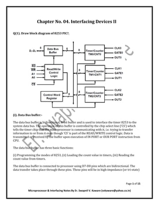
  • 1. Page 1 of 15 Microprocessor & Interfacing Notes By Er. Swapnil V. Kaware (svkaware@yahoo.co.in) Chapter No. 04. Interfacing Devices II Q(1). Draw block diagram of 8253 PIC?. (i). Data Bus buffer:- The data bus buffer is bidirectional, 8-bit buffer and is used to interface the timer 8253 to the system data bus. The operation of this buffer is controlled by the chip select line (‘CS’) which tells the timer chip that the microprocessor is communicating with it, i.e. trying to transfer information to or from it even though ‘CS’ is part of the READ/WRITE control logic. Data is transmitted or received by the buffer upon execution of IN PORT or OUR PORT instruction from CPU. The data bus buffer has three basic functions: (i) Programming the modes of 8253, (ii) Loading the count value in timers, (iii) Reading the count value from timers. The data bus buffer is connected to processor using D7-D0 pins which are bidirectional. The data transfer takes place through these pins. These pins will be in high-impedance (or tri-state)
  • 2. Page 2 of 15 Microprocessor & Interfacing Notes By Er. Swapnil V. Kaware (svkaware@yahoo.co.in) condition until the 8253 is selected by a LOW on CS and either the read operation requested by a LOW on the R D input or a write operation requested by the WR input going LOW. Read/ Write Logic: It accepts inputs for the system control bus and in turn generates the control signals for overall device operation. It is enabled or disabled by C S so that no operation can occur to change the function unless the device has been selected by the system logic. CS:- The chip select input is used to enable the communication between 8253 chip and the microprocessor by means of data bus. A low on C S enables the data bus buffers, while a high disables the buffer. The CS input does not have any affect on the operation of three timers once they have been initialized. The normal configuration of a system employs some decoding logic which actives CS line, whenever a specific set of addresses that correspond to 8253 appear on the address bus. RD & WR: - The read (‘RD’) and write (‘WR’) pins control the direction of data transfer on the 8-bit bus. When the RD input pin is low, then CPU is reading data from 8253 in the form of counter value. When WR pin is low, then CPU is writing data to 8253 in the form of mode information or loading initial count values to counters. The RD & WR should not both be low simultaneously. When RD & WR signals are HIGH, the data bus buffer is disabled and no data transfer takes place between processor and 8253. A0 & A1: These two input lines allow the microprocessor to specify which one of the internal register in the 8253 is going to be used for the data transfer. Fig shows how these two lines are used to select either the control word register or one of the 16-bit counters. For example, if there is a, “1” on both A0 & A1, and a “0‟ on WR , then the processor is writing a control word to the control word register. These two pins are usually connected to the address bus lines, normally of the same name (A0 & A1). A1 A0 RD WR CS Result 0 0 1 0 0 Write Counter 0 0 1 1 0 0 Write Counter 1 1 0 1 0 0 Write Counter 2
  • 3. Page 3 of 15 Microprocessor & Interfacing Notes By Er. Swapnil V. Kaware (svkaware@yahoo.co.in) 1 1 1 0 0 Write Control Word 0 0 0 1 0 Read Counter 0 0 1 0 1 0 Read Counter 1 1 0 0 1 0 Read Counter 2 1 1 0 1 0 No operation X X 1 1 0 No operation X X X X 1 No operation Control Word Register: - The control word register is used to program the timers in different modes and control their operations. It is selected when A0 and A1 pins are 1 & 1‟. If WR is also low, it accepts information from the data bus buffer and stores it in control word register. The information stored then controls the operation mode of each counter, selection of binary or BCD counting and the loading of each counting and the loading of each count register. This register can be written into only; no read operation of this content is available. The format will be discussed later on. Counters:- Each of the timers has three pins associated with it. These are clock (CLK) input, the gate (GATE) control input and the output (OUT). CLK:- This clock input pin provides 16-bit timer with the signal that causes the timer to decrement. The maximum clock frequency input is 2.6MHz. Note that the counters operate at HIGH to LOW transition (the negative edge) of this clock input. If the signal on this pin is generated by a fixed frequency oscillator then the user has implemented a standard timer for getting the desired delay. The count value to be loaded, in this case, determines the delay produced by the timer. If the input signal is a string of randomly occurring pulses, then it is called implementation of a counter. In this case, these clock pulses occur whenever an event takes place. Whenever a negative transition occurs at CLK input, the count value is decremented. From initial and value one can count the number of times an event has taken place in an interval.
  • 4. Page 4 of 15 Microprocessor & Interfacing Notes By Er. Swapnil V. Kaware (svkaware@yahoo.co.in) GATE:- The gate input pin is used to initiate or enable counting. The exact effect of the gate signal depends on which of the six modes of operation is chosen. OUTPUT:- The output pin provides an output from the timer. Its actual use depends on the mode of operation of the timer. The counter can be read “on the fly” without inhibiting gate pulse or clock input. The timers are 16-bit down counters. These timers are loaded with an initial value before triggering. Every high to low transition at CLK input decrements the count by one. The operation of timers can be best understood by considering the internal structure of timer. Each timer is having three elements- input element (IE), counting element (CE) and output element (OE). Q(2). Draw & explain Control word format of 8253 PIC?.
  • 5. Page 5 of 15 Microprocessor & Interfacing Notes By Er. Swapnil V. Kaware (svkaware@yahoo.co.in) Q(3). Explain Various modes of operation of 8253 PIC?. 8253/54 can be operated in 6 different modes. (i).Mode0─InterruptonTerminalCount:- It is used to generate an interrupt to the microprocessor after a certain interval. Initially the output is low after the mode is set. The output remains LOW after the count value is loaded into the counter. The process of decrementing the counter continues till the terminal count is reached, i.e., the count become zero and the output goes HIGH and will remain high until it reloads a new count. The GATE signal is high for normal counting. When GATE goes low, counting is terminated and the current count is latched till the GATE goes high again. (ii).Mode1–ProgrammableOneShot:- It can be used as a mono stable multi-vibrator. The gate input is used as a trigger input in this mode. The output remains high until the count is loaded and a trigger is applied. (iii).Mode2–RateGenerator:-
  • 6. Page 6 of 15 Microprocessor & Interfacing Notes By Er. Swapnil V. Kaware (svkaware@yahoo.co.in) The output is normally high after initialization. Whenever the count becomes zero, another low pulse is generated at the output and the counter will be reloaded. (iv).Mode3–SquareWaveGenerator:- This mode is similar to Mode 2 except the output remains low for half of the timer period and high for the other half of the period. (v).Mode4−SoftwareTriggeredMode:- In this mode, the output will remain high until the timer has counted to zero, at which point the output will pulse low and then go high again. The count is latched when the GATE signal goes LOW. On the terminal count, the output goes low for one clock cycle then goes HIGH. This low pulse can be used as a strobe. (vi). Mode5–HardwareTriggeredMode:-
  • 7. Page 7 of 15 Microprocessor & Interfacing Notes By Er. Swapnil V. Kaware (svkaware@yahoo.co.in) This mode generates a strobe in response to an externally generated signal. This mode is similar to mode 4 except that the counting is initiated by a signal at the gate input, which means it is hardware triggered instead of software triggered. After it is initialized, the output goes high. When the terminal count is reached, the output goes low for one clock cycle. Q(4). Draw and explain block diagram of 8275 CRT controller?.
  • 8. Page 8 of 15 Microprocessor & Interfacing Notes By Er. Swapnil V. Kaware (svkaware@yahoo.co.in) Q(5). Draw & explain block diagram of 8237 DMA controller?. Direct Memory Access (DMA) is a method of allowing data to be moved from one location to another in a computer without intervention from the central processor (CPU). It is also a fast way of transferring data within (and sometimes between) computer. The DMA I/O technique provides direct access to the memory while the microprocessor is temporarily disabled. The DMA controller temporarily borrows the address bus, data bus and control bus from the
  • 9. Page 9 of 15 Microprocessor & Interfacing Notes By Er. Swapnil V. Kaware (svkaware@yahoo.co.in) microprocessor and transfers the data directly from the external devices to a series of memory locations (and vice versa). DMA Operation:- Two control signals are used to request and acknowledge a direct memory access (DMA) transfer in the microprocessor-based system. The HOLD signal as an input(to the processor) is used to request a DMA action. The HLDA signal as an output that acknowledges the DMA action When the processor recognizes the hold, it stops its execution and enters hold cycles. HOLD input has higher priority than INTR or NMI. The only microprocessor pin that has a higher priority than a HOLD is the RESET pin. HLDA becomes active to indicate that the processor has placed its buses at high-impedance state. Direct memory accesses normally occur between an I/O device and memory without the use of the microprocessor. A DMA read transfers data from the memory to the I/O device. A DMA write transfers data from an I/O device to memory. The system contains separate memory and I/O control signals. Hence the Memory & the I/O are controlled simultaneously. The DMA controller provides memory with its address, and the controller signal selects the I/O device during the transfer. Data transfer speed is determined by speed of the memory device or a DMA controller. In many cases, the DMA controller slows the speed of the system when transfers occur. The serial PCI (Peripheral Component Interface) Express bus transfers data at rates exceeding DMA transfers. This in modern systems has made DMA is less important. The 8237 supplies memory & I/O with control signals and memory address information during the DMA transfer. It is actually a special-purpose microprocessor whose job is high-speed data transfer between memory and I/O.
  • 10. Page 10 of 15 Microprocessor & Interfacing Notes By Er. Swapnil V. Kaware (svkaware@yahoo.co.in) Q(6). Draw & explain block diagram of 8237 DMA controller?. Q(7). Explain various operating modes of 8237 DMA controller?. A single byte (or word) is transferred. The DMA must release and re-acquire the bus for each additional byte. This is commonly-used by devices that cannot transfer the entire block of data immediately. The peripheral will request the DMA each time it is ready for another transfer. The floppy disk controller only has a one-byte buffer, so it uses this mode. (i). Block/Demand mode:- Once the DMA acquires the system bus, an entire block of data is transferred, up to a maximum of 64K. If the peripheral needs additional time, it can assert the READY signal. READY should not be used excessively, and for slow peripheral transfers, the Single Transfer Mode should be used instead. The difference between Block and Demand is the once a Block transfer is started, it runs until the transfer count reaches zero. DRQ only needs to be asserted until -DACK is asserted. Demand Mode will transfer one more bytes until DRQ is de-asserted, then when DRQ is asserted later, the transfer resumes where it was suspended. Older hard disk controllers used Demand Mode until CPU speeds increased to the point that it was more efficient to read the data using the CPU.
  • 11. Page 11 of 15 Microprocessor & Interfacing Notes By Er. Swapnil V. Kaware (svkaware@yahoo.co.in) (ii). Cascade mode:- This mechanism allows a DMA channel to request the bus, but then the attached peripheral device is responsible for placing addressing information on the bus. This is also known as ``Bus Mastering''. When a DMA channel in Cascade Mode receives control of the bus, the DMA does not place addresses and I/O control signals on the bus like it normally does. Instead, the DMA only asserts the -DACK signal for this channel. Now it is up to the device connected to that DMA channel to provide address and bus control signals. The peripheral has complete control over the system bus, and can do reads and/or writes to any address below 16Meg. When the peripheral is finished with bus, it de-asserts the DRQ line, and the DMA controller can return control to the CPU or to some other DMA channel. Cascade Mode can be used to chain multiple DMA controllers together, and this is exactly what DMA Channel 4 is used for in the PC. When a peripheral requests the bus on DMA channels 0, 1, 2 or 3, the slave DMA controller asserts HLDREQ, but this wire is actually connected to DRQ4 on the primary DMA controller. The primary DMA controller then requests the bus from the CPU using HLDREQ. (iv). Autoinitialize mode:- This mode causes the DMA to perform Byte, Block or Demand transfers, but when the DMA transfer counter reaches zero, the counter and address is set back to where they were when the DMA channel was originally programmed. This means that as long as the device requests transfers, they will be granted. It is up to the CPU to move new data into the fixed buffer ahead of where the DMA is about to transfer it for output operations, and read new data out of the buffer behind where the DMA is writing on input operations. This technique is frequently used on audio devices that have small or no hardware ``sample'' buffers. There is additional CPU overhead to manage this ``circular'' buffer, but in some cases this may be the only way to eliminate the latency that occurs when the DMA counter reaches zero and the DMA stops until it is reprogrammed. Q(8). Internal architecture of 8086 microprocessor?. OR Q(9). Explain various registers of 8086 microprocessor?. 8086 Microprocessor is divided into two functional units, i.e., EU (Execution Unit) and BIU (Bus Interface Unit). Execution Unit:- The Execution unit is responsible for decoding and executing all instructions. The EU extracts instructions from the top of the queue in the BIU, decodes them, generates operands if necessary, passes them to the BIU and requests it to perform the read or write bys cycles to memory or I/O and perform the operation specified by the instruction on the operands.
  • 12. Page 12 of 15 Microprocessor & Interfacing Notes By Er. Swapnil V. Kaware (svkaware@yahoo.co.in) During the execution of the instruction, the EU tests the status and control flags and updates them based on the results of executing the instruction. If the queue is empty, the EU waits for the next instruction byte to be fetched and shifted to top of the queue. When the EU executes a branch or jump instruction, it transfers control to a location corresponding to another set of sequential instructions. Whenever this happens, the BIU automatically resets the queue and then begins to fetch instructions from this new location to refill the queue. ALU:- It handles all arithmetic and logical operations, like +, −, ×, /, OR, AND, NOT operations. Flag Register:-
  • 13. Page 13 of 15 Microprocessor & Interfacing Notes By Er. Swapnil V. Kaware (svkaware@yahoo.co.in) It is a 16-bit register that behaves like a flip-flop, i.e. it changes its status according to the result stored in the accumulator. It has 9 flags and they are divided into 2 groups − Conditional Flags and Control Flags. Conditional Flags:- It represents the result of the last arithmetic or logical instruction executed. Following is the list of conditional flags, Carry flag − This flag indicates an overflow condition for arithmetic operations. Auxiliary flag − When an operation is performed at ALU, it results in a carry/barrow from lower nibble (i.e. D0 – D3) to upper nibble (i.e. D4 – D7), then this flag is set, i.e. carry given by D3 bit to D4 is AF flag. The processor uses this flag to perform binary to BCD conversion. Parity flag − This flag is used to indicate the parity of the result, i.e. when the lower order 8- bits of the result contains even number of 1’s, then the Parity Flag is set. For odd number of 1’s, the Parity Flag is reset. Zero flag − This flag is set to 1 when the result of arithmetic or logical operation is zero else it is set to 0. Sign flag − This flag holds the sign of the result, i.e. when the result of the operation is negative, then the sign flag is set to 1 else set to 0. Overflow flag − This flag represents the result when the system capacity is exceeded. Control Flags:- Control flags controls the operations of the execution unit. Following is the list of control flags, Trap flag − It is used for single step control and allows the user to execute one instruction at a time for debugging. If it is set, then the program can be run in a single step mode. Interrupt flag − It is an interrupt enable/disable flag, i.e. used to allow/prohibit the interruption of a program. It is set to 1 for interrupt enabled condition and set to 0 for interrupt disabled condition. Direction flag − It is used in string operation. As the name suggests when it is set then string bytes are accessed from the higher memory address to the lower memory address and vice-a- versa.
  • 14. Page 14 of 15 Microprocessor & Interfacing Notes By Er. Swapnil V. Kaware (svkaware@yahoo.co.in) General purpose register:- There are 8 general purpose registers, i.e., AH, AL, BH, BL, CH, CL, DH, and DL. These registers can be used individually to store 8-bit data and can be used in pairs to store 16bit data. The valid register pairs are AH and AL, BH and BL, CH and CL, and DH and DL. It is referred to the AX, BX, CX, and DX respectively. AX register − It is also known as accumulator register. It is used to store operands for arithmetic operations. BX register − It is used as a base register. It is used to store the starting base address of the memory area within the data segment. CX register − It is referred to as counter. It is used in loop instruction to store the loop counter. DX register − This register is used to hold I/O port address for I/O instruction. Stack pointer register:- It is a 16-bit register, which holds the address from the start of the segment to the memory location, where a word was most recently stored on the stack. BIU(BusInterfaceUnit):- The Bus Interface Unit contains Bus Interface Logic, Segment registers, Memory addressing logic and a Six byte instruction object code queue. The BIU sends out address, fetches the instructions from memory, read data from ports and memory, and writes the data to ports and memory. BIU takes care of all data and addresses transfers on the buses for the EU like sending addresses, fetching instructions from the memory, reading data from the ports and the memory as well as writing data to the ports and the memory. EU has no direction connection with System Buses so this is possible with the BIU. EU and BIU are connected with the Internal Bus. It has the following functional parts, Instruction queue − BIU contains the instruction queue. BIU gets up to 6 bytes of next instructions and stores them in the instruction queue. When EU executes instructions and is ready for its next instruction, then it simply reads the instruction from this instruction queue resulting in increased execution speed. Fetching the next instruction while the current instruction executes is called pipelining. Segment register − BIU has 4 segment buses, i.e. CS, DS, SS & ES. It holds the addresses of instructions and data in memory, which are used by the processor to access memory locations. It also contains 1 pointer register IP, which holds the address of the next instruction to executed by the EU.
  • 15. Page 15 of 15 Microprocessor & Interfacing Notes By Er. Swapnil V. Kaware (svkaware@yahoo.co.in) CS − It stands for Code Segment. It is used for addressing a memory location in the code segment of the memory, where the executable program is stored. DS − It stands for Data Segment. It consists of data used by the program andis accessed in the data segment by an offset address or the content of other register that holds the offset address. SS − It stands for Stack Segment. It handles memory to store data and addresses during execution. ES − It stands for Extra Segment. ES is additional data segment, which is used by the string to hold the extra destination data. Instruction pointer − It is a 16-bit register used to hold the address of the next instruction to be executed. ***************************************** ALL THE BEST *****************************************